Abstract
Adder is an important datapath unit of a general-purpose microprocessor or a digital signal processor. In the nanoelectronics era, the design of an adder that is modular and which can withstand variations in process, voltage and temperature are of interest. In this context, this article presents a new robust early output asynchronous block carry lookahead adder (BCLA) with redundant carry logic (BCLARC) that has a reduced power-cycle time product (PCTP) and is a low power design. The proposed asynchronous BCLARC is implemented using the delay-insensitive dual-rail code and adheres to the 4-phase return-to-zero (RTZ) and the 4-phase return-to-one (RTO) handshaking. Many existing asynchronous ripple-carry adders (RCAs), carry lookahead adders (CLAs) and carry select adders (CSLAs) were implemented alongside to perform a comparison based on a 32/28 nm complementary metal-oxide-semiconductor (CMOS) technology. The 32-bit addition was considered for an example. For implementation using the delay-insensitive dual-rail code and subject to the 4-phase RTZ handshaking (4-phase RTO handshaking), the proposed BCLARC which is robust and of early output type achieves: (i) 8% (5.7%) reduction in PCTP compared to the optimum RCA, (ii) 14.9% (15.5%) reduction in PCTP compared to the optimum BCLARC, and (iii) 26% (25.5%) reduction in PCTP compared to the optimum CSLA.
1. Introduction
In the nanoelectronics era, design-for-manufacturability issues such as process variability due to process-induced defects, device variability due to random dopant and atomistic fluctuations, hot carrier effects, negative bias temperature instability, stress-induced variation, electrostatic discharge etc. and other metrology issues are more pronounced compared to the microelectronics era [1,2]. As a result, the synchronous design method may involve more than a 100% overhead [3] in specifying the practical timing of a digital circuit or system. This is to compensate for any or a combination of the clock network delay, the clock jitter, unexpected statistical timing variation(s) of the combinational logic, storage elements and control logic etc. [4]. In this backdrop, an asynchronous design method that is modular and which can innately cope with arbitrary variations in processes or parameters is preferable [5,6,7]. Such an asynchronous design method corresponds to the input-output timing model [8], which utilizes delay-insensitive codes for data encoding (i.e., representation) and processing and adheres to the 4-phase return-to-zero (RTZ) or return-to-one (RTO) handshake protocol for data communication. An illustration of such an asynchronous circuit stage sandwiched between the data sender and the receiver is given in Figure 1.
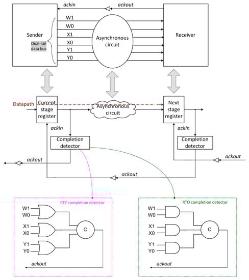
Figure 1.
An asynchronous circuit stage present between two register stages (current and next) is correlated with the sender and receiver analogy. An example dual-rail data bus consisting of the encoded inputs (W1, W0), (X1, X0) and (Y1, Y0) is shown. The datapath is highlighted in brown dashed lines. The completion detectors, which would indicate i.e., acknowledge the receipt of the primary inputs, corresponding to the 4-phase return-to-zero (RTZ) and return-to-one (RTO) handshaking are also shown. The circle with the marking ‘C’ represents the (symmetric) Muller C-element.
In Figure 1, the sender and the receiver comprise registers, which are constructed using 2-input Muller C-elements. C-elements are also called registers since they are fundamentally elements with memory. One of the inputs to the 2-input C-element (i.e., register) is the ackin signal and the other is an encoded data input rail. The Muller C-element [9] is an important building block of asynchronous circuits. The C-element would output 0 or 1 if all its inputs are 0 or 1 respectively and would maintain its existing state if its inputs are not identical. The data communication between the sender and the receiver i.e., handshaking is performed by involving either an intermediate RTZ [10] or an intermediate RTO [11] of the encoded data wires. The former is called 4-phase RTZ handshaking and the latter is called 4-phase RTO handshaking. The 4-phase RTZ or the 4-phase RTO handshake protocol can be used for data communication between the input and output registers of an asynchronous circuit stage as shown in Figure 1. We shall first discuss the delay-insensitive dual-rail data encoding in the context of the 4-phase RTZ handshaking followed by the 4-phase RTO handshaking.
1.1. Dual-Rail Data Encoding and 4-Phase RTZ Handshaking
In Figure 1, the inputs and outputs of the asynchronous circuit are dual-rail encoded [12]. For example, the data wire W is encoded as W1 and W0. According to the 4-phase RTZ handshaking [10], W = 1 is represented as W1 = 1 and W0 = 0 and W = 0 is represented as W1 = 0 and W0 = 1. These two combinations represent the data. W1 = W0 = 0 is called the spacer. W1 = W0 = 1 is deemed to be illegal since the delay-insensitive coding scheme should be unordered [13]. In Figure 1, ackin and ackout represent the acknowledgment input and output signals of the asynchronous circuit stage, and ackin is the Boolean complement of ackout. There is no explicit provision of a data request wire since the data request is embedded within the encoded data wires.
In accordance with the 4-phase RTZ handshake protocol, the inputs are applied as follows: data-spacer-data-spacer and so forth. Each application of input data is succeeded by a RTZ of the encoded data wires. The 4-phase RTZ handshaking process is described using the following steps.
- In the first phase, the dual-rail data bus specified by (W1, W0) etc., is in the spacer state and ackin is 1. After the sender transmits a data, this would result in rising signal transitions i.e., binary 0 to 1 on one of the dual rails of the dual-rail data bus.
- In the second phase, the receiver receives the data sent and drives ackout to 1.
- In the third phase, the sender waits for ackin to become 0 and then resets the dual-rail data bus to the spacer state (i.e., all 0 s).
- In the fourth phase, after an unbounded, finite and positive time duration, the receiver drives ackout to 0 and subsequently ackin would assume 1. One data transaction is now said to be complete, and the asynchronous circuit may start the next data transaction.
1.2. Dual-Rail Data Encoding and 4-Phase RTO Handshaking
According to the 4-phase RTO handshake protocol [11], the dual-rail data encoding is done as follows. For example, the data W = 1 is represented as W1 = 0 and W0 = 1 and the data W = 0 is represented as W0 = 0 and W1 = 1. The spacer is represented as W0 = W1 = 1, and W0 = W1 = 0 is deemed to be illegal. In accordance with the 4-phase RTO protocol, the application of inputs to an asynchronous circuit follows this sequence: spacer-data-spacer-data, and so forth with each application of input data succeeded by a RTO of the encoded data wires. The 4-phase RTO handshaking process is described as follows:
- In the first phase ackin is 1. After the sender transmits the spacer i.e., all 1 s, this would cause rising signal transitions on all the rails of the dual-rail data bus.
- In the second phase, the receiver receives the spacer sent, and drives ackout to 1.
- In the third phase, the sender waits for ackin to assume 0, and transmits the input data by resetting any one of the respective dual-rails of the dual-rail data bus.
- In the fourth phase, after an unbounded but positive and finite time duration, the receiver would drive ackout to 0 and ackin would assume 1. With this one data transaction is said to be complete, and the asynchronous circuit stage may start the next data transaction.
2. Input-Output Mode Asynchronous Circuits
2.1. Types
Input-output mode asynchronous circuits are commonly categorized into four types as strong indication [14,15], weak indication [14,16], early output [17], and relative timed [18]. The degree of robustness would follow the descending order of hierarchy listed. But the optimizations achievable in the design metrics generally follows the ascending order of the hierarchy. Of the four types listed, strong indication, weak indication, and early output asynchronous circuits are robust when they incorporate quasi-delay-insensitive (QDI) logic decomposition. In this context, strong indication, weak indication, and early output asynchronous circuits are said to be QDI. QDI circuits represent the practical implementation of delay-insensitive asynchronous circuits by assuming the presence of isochronic forks [19]. The isochronic fork represents the weakest compromise to delay-insensitivity. An isochronic fork assumption implies that all the wire branches forking out from a node/junction experience concurrent signal transitions whether they are rising or falling. Reference [20] showed that isochronic forks are realizable in the nanoelectronics regime which implies that the QDI circuit implementations are feasible. QDI circuit/system implementations may also be feasible in emerging technologies such as silicon nanowire field-effect transistors (FETs) and graphene SymFETs [1]. In [21,22] the utility of these emerging technologies for hardware security applications based on the synchronous design method was investigated and it was concluded that they can outperform the CMOS technology. Relative timed circuits tend to incorporate additional timing assumptions besides the assumption of isochronic forks, which are likely to be sophisticated (complicated). If the additional timing assumptions made in a relative timed circuit are violated, then the circuit would not be practically robust. Extensive timing verification and engineering effort may be required to realize a relative timed circuit and despite these, a relative timed circuit may fail if the timing assumptions introduced are violated due to process and/or parametric variations. Hence, relative timed circuits are not QDI.
The input-output timing characteristics of various types of asynchronous circuits are portrayed in Figure 2, corresponding to the 4-phase RTZ and RTO handshake protocols.
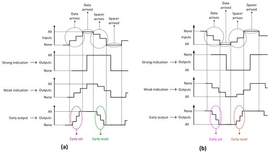
Figure 2.
Timing behavior of strong indication, weak indication, and early output asynchronous circuits corresponding to: (a) RTZ handshaking; (b) RTO handshaking.
Strong indication circuits would wait for the arrival of all the primary inputs (whether they are data or spacer) after which they would process the data received to produce the primary outputs. A composition of strong indication sub-circuits may yield a weak indication circuit. For example, a connection of two strong indication full adders would result in a 2-bit weak indication RCA. This is because if all the inputs to one full adder would arrive then the sum and carry output bits of that full adder could be produced regardless of the non-arrival of the inputs to the other full adder.
Weak indication circuits can produce all but one of the primary outputs after receiving a subset of the primary inputs. Nevertheless, only after receiving the last primary input, the last primary output is produced. A composition of weak indication sub-circuits leads to a weak indication circuit. On the other hand, a composition of strong and weak indication sub-circuits would also result in a weak indication circuit.
Early output circuits can produce all the primary outputs (data or spacer) after receiving just a subset of the primary inputs. If an early output circuit produces the data early, it is called early set type. On the contrary, if an early output circuit produces the spacer early, it is called early reset type. The early set and reset behaviors are captured within the violet and green ellipses in Figure 2a corresponding to the RTZ handshaking, and they are captured within the pink and brown dotted ellipses in Figure 2b corresponding to the RTO handshaking. A homogeneous composition of early output sub-circuits or a heterogeneous composition of strong indication and/or weak indication and early output sub-circuits would result in an early output circuit of the same kind as that of the early output sub-circuits comprising it.
Relative timed circuits correspond to the early output type but are not QDI. However, as mentioned earlier, relative timed asynchronous circuits would tend to incorporate additional timing assumptions to guarantee their safe operation, and they are the least robust of the input-output mode asynchronous circuits. Nevertheless, they are likely to facilitate better optimizations in the design metrics compared to their counterparts. Hence, when deciding to choose relative timing for realizing computer arithmetic, there would be a trade-off between robustness and the quality of results. However, to achieve the twin objectives of robustness and good quality of results, the early output type may be preferred. Nevertheless, this observation may not be universally applicable for the asynchronous realization of different kinds of computer arithmetic since the phenomenon of robustness may also depend on the arithmetic circuit structure to be realized in asynchronous style.
2.2. Characteristics
Asynchronous circuits featuring delay-insensitive data encoding and adhering to a 4-phase handshaking (RTZ or RTO) for data communication usually embed the monotonic cover constraint (MCC) [10] in their underlying logic. To briefly explain what is the MCC, let us consider the dual-rail encoded realization of a 2-input AND function shown in Figure 3, corresponding to the 4-phase RTZ handshaking. (A1, A0) and (B1, B0) represent the dual-rail encoded primary inputs and (Y1, Y0) represents the dual-rail encoded primary output. The circles with the markings C1, C2, C3 and C4 in Figure 3 represent the 2-input Muller C-elements.
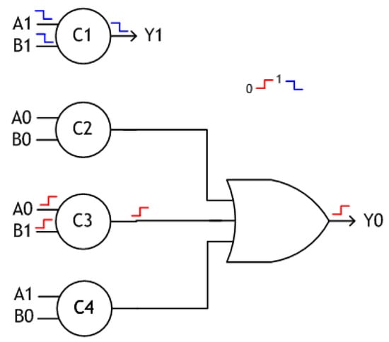
Figure 3.
2-input AND function realized using the delay-insensitive minterm synthesis (DIMS) method, conforming to RTZ handshaking.
The logic expressions for the 2-input AND function are given below, which correspond to the delay-insensitive minterm synthesis (DIMS) method [23]. Equation (1) contains only one product term, which signifies the monotonic cover. On the other hand, (2) contains three product terms but the cover constraint is still monotonic. This means only one out of the three product terms in (2) would be activated for the application of appropriate input data, and the rest of the product terms would remain deactivated. This is because the product terms constituting (2) are disjoint. In a disjoint sum-of-products expression [24], the products are mutually orthogonal and the logical conjunction of any two products would yield 0.
Y1 = A1B1
Y0 = A0B0 + A0B1 + A1B0
Figure 3 also portrays two example input scenarios. Let us first assume that A0 and B1 experience rising signal transitions i.e., A0 = B1 = 1 during a data phase i.e., after a spacer phase where A0 and B1 were equal to 0. This would cause a rising signal transition to occur on the output of C3, which would be followed by a rising signal transition on the primary output rail Y0. Thus, the rising signal transitions on A0 and B1 are unambiguously indicated (i.e., acknowledged) by the primary output rail Y0 while involving the intermediate gate output of C3. Let us now consider falling signal transitions on the inputs A1 and B1 i.e., A1 = B1 = 0 after a data phase where A1 and B1 were equal to 1 earlier. This would result in the reset of Y1 i.e., Y1 = 0. These two example input scenarios show that the signal transitions occur monotonically throughout the circuit [25], i.e., the signals monotonically increase for the application of input data and they monotonically decrease for the application of the spacer throughout the entire circuit from the primary inputs up to the primary outputs, in conformance with the RTZ handshake protocol. In the case of RTO handshaking, the transitions would monotonically increase for the application of the spacer and would monotonically decrease for the application of the data.
The non-acknowledgment of a signal transition on a wire is called wire orphan and the non-acknowledgment of a signal transition on the output of a gate is called gate orphan [26]. Wire orphans are less problematic than the gate orphans. Wire orphans may arise in a circuit, but they can be overcome by imposing the isochronic fork assumption. Gate orphans, even if they are likely to occur in a circuit, as is the case with most relative timed circuits, can be avoided by making certain timing assumptions which however might be sophisticated to realize and may complicate the circuit verification aspect. Nevertheless, if the environment is assumed to be rather slow changing then the gate level realization is likely to be safe [27].
To shed the light on wire and gate orphans, we refer to Figure 4. Figure 4 shows a gate-level implementation of an example Boolean function F, expressed as F = PQ + RS, where P, Q, R and S are the primary inputs. A dual-rail logic equivalent that corresponds to the early output type is shown where F1 = P1Q1 + R1S1 and F0 = (P0 + Q0) (R0 + S0). The gate pairs (G4, G5), (G6, G7), and (G8, G9) form the respective early output logic equivalents of the gates G1, G2, and G3. X and Y are the intermediate single-rail outputs, and (X1, X0) and (Y1, Y0) are the intermediate dual-rail outputs.
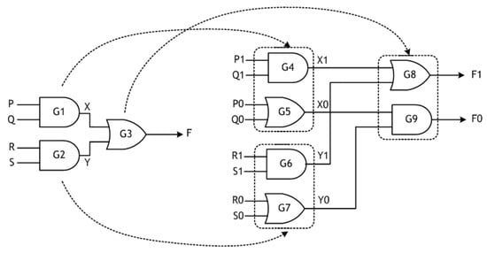
Figure 4.
Dual-rail early output type asynchronous realization of the logic function F = PQ + RS, corresponding to RTZ handshaking.
Figure 4 serves to illustrate the need for the proper indication of signal transitions at the primary inputs and the intermediate (gate) outputs and points out how wire and gate orphans can probably occur for an example RTZ handshaking. However, the following discussion is applicable for a circuit corresponding to the RTO handshaking.
If the data inputs are currently assumed to be spacers, and in the next data phase, if P0 and R0 assume 1, the intermediate outputs X0 and Y0 would be driven to 1 and eventually F0 would assume 1. If Q0 and S0 also assume 1, but later, these signal transitions will not be acknowledged by the intermediate outputs or by the primary output in the current data evaluation phase leading to the occurrence of wire orphans because of the belated signal transitions on the inputs Q0 and S0. However, the wire orphans arising on the inputs Q0 and S0 can be overcome by imposing the isochronicity assumption on Q0 and S0.
Let us consider another scenario where P1 and Q1 assume 1 after a RTZ phase. This would result in X1 to be driven to 1. If R1 and S1 also assume 1, but later in the current evaluation phase, Y1 would become 1. However, F1 could have assumed 1 just because of X1 having become 1 and so the late signal transition on Y1 will not be acknowledged by the primary output (F1) resulting in the occurrence of a gate orphan. This gate orphan problem may be eliminated by assuming that Y1 becomes 1 before F1 could assume 1, which is a complicated relative timing assumption.
References [28,29,30] discuss other scenarios as to how gate orphans could occur due to the unsafe logic decomposition of a high fan-in OR gate and a high fan-in C-element. In general, gate orphans should be avoided in the multi-level synthesis of asynchronous circuits to ensure the robustness. One way of avoiding the gate orphans is by adhering to (safe) QDI logic decomposition principles, which are described in [29,30,31]. The assumption of isochronic forks is essential to practically implement asynchronous circuits belonging to strong indication, weak indication, and early output types. However, such circuits should have to be free of gate orphan(s) to be identified as robust, and this could be guaranteed by resorting to (safe) QDI logic decomposition. In the case of relative timed circuits, gate orphans are more likely to occur and to overcome any potential problem due to those, additional timing assumptions may have to be incorporated which could complicate the physical realization. Nevertheless, despite the extra timing assumptions imposed besides the assumption of isochronic forks, relative timed circuits are not guaranteed to be robust.
3. Datapaths Traversed in Asynchronous Adders
Ripple-carry adder (RCA), carry lookahead adder (CLA), and carry select adders (CSLA) architectures were considered for the asynchronous implementations of 32-bit addition. The building blocks used for the adder implementations such as the block carry lookahead generator without redundant carry output (BCLG), the block carry lookahead generator with redundant carry output (BCLGRC), the recursive 4-bit CLA, the full adder, the sum logic etc. correspond to strong indication, weak indication, and early output timing models.
Figure 5 and Figure 6 portray the various adder architectures. The numeral indices 31 and 0 denote the most significant and the least significant adder bit positions. Dual-rail encoded A31 to A0 and B31 to B0 represent the adder inputs, and dual-rail encoded SUM31 to SUM0 represents the sum output. ‘C’ refers to carry and ‘RC’ refers to redundant carry. Figure 5 depicts the RCA and CSLA architectures. Figure 6 portrays the block carry lookahead adder (BCLA), also called the section-carry based carry lookahead adder, and the recursive CLA (RCLA) architectures.
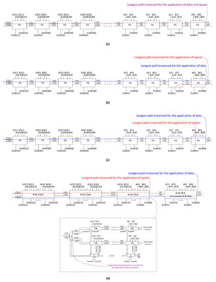
Figure 5.
Longest datapaths traversed for the application of data and spacer in: (a) 32-bit ripple-carry adder (RCA) comprising strong indication full adders [23,32] or distributed weak indication full adders [33]; (b) 32-bit RCA comprising biased weak indication [28,34] or early output full adders [35]; (c) 32-bit relative timed RCA comprising early output full adders [36]; (d) an optimum 32-bit early output carry select adder (CSLA) [37]. FA refers to the full adder, and 2:1 MUX refers to the two-input multiplexer in the figures.
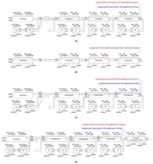
Figure 6.
‘FA’, ‘SL’, ‘BCLG’ and ‘RCLA’ refer to the full adder, sum logic, block carry lookahead generator, and recursive carry lookahead adder in the figure. (a) 32-bit BCLA [39]; (b) 32-bit RCLA [41]; (c) 32-bit BCLARC [40]; (d) 32-bit hybrid BCLARC-RCA [40].
Figure 5 and Figure 6 show the fundamental differences between the respective adder architectures and show the datapaths traversed in the various adders for the application of the data and the spacer. This is important to note because in the case of synchronous designs the maximum (also called the longest or the worst-case or the critical) datapath delay determines the speed of operation of a synchronous circuit. However, in an asynchronous circuit incorporating delay-insensitive data encoding and adhering to a 4-phase RTZ or RTO handshaking for data communication, the ‘cycle time’ determines the speed of operation i.e., the speed at which new data can be input to an asynchronous circuit. The cycle time is composed of two timing metrics namely the forward latency and the reverse latency. Forward latency is the time taken to process the data, which is akin to the critical path delay of a synchronous circuit, and the reverse latency is the time taken to process the spacer. The sum of forward and reverse latencies is the cycle time. In Figure 5 and Figure 6, the datapaths traversed corresponding to the worst-case forward latency are highlighted in blue dotted lines, and the datapaths traversed corresponding to the worst-case reverse latency are highlighted in red dotted lines. The violet dotted lines signify that the datapaths traversed in an adder are the same for the application of the data (corresponding to forward latency) and the spacer (corresponding to reverse latency).
Figure 5a–c are asynchronous RCAs, which are constructed by cascading the full adders belonging to strong indication [23,32], weak indication [28,33,34], and early output [35] types. The RCAs are grouped in Figure 5 according to the longest datapaths traversed for the application of the data (corresponding to forward latency) and the spacer (corresponding to reverse latency). It is mentioned in [36] that a RCA featuring strong indication full adders would encounter the worst-case forward and reverse latencies; a RCA comprising distributed weak indication full adders may experience data-dependent forward and reverse latencies; a RCA having biased weak indication or early output full adders would experience a data-dependent forward latency and a constant reverse latency of two full adder delays; and a relative timed RCA incorporating early output full adders would experience a data-dependent forward latency and the minimal constant reverse latency of one full adder delay.
From the perspectives of latencies and more importantly from the perspective of cycle time, a relative timed RCA is quite preferable to its early output counterpart but there is a trade-off of the robustness since the former is not QDI and hence less robust than the latter which is QDI. Further, as noted in [36], the relative-timed RCAs presented exhibit a negative timing slack, which do not guarantee a safe operation.
Figure 5d shows an optimum 32-bit asynchronous CSLA [37], realized based on a uniform 8-8-8-8 input partition, which is constructed using early output full adders [35] and strong indication two-input multiplexers [38]. The internals of an 8-bit sub-CSLA is shown in Figure 5d and the datapath that will be traversed within a constituent 8-bit CSLA for the application of the data and the spacer would be the same, which is highlighted by the violet dotted lines.
Figure 6a shows the implementation of 32-bit weak indication [28,34,39], and early output [35,40] robust BCLAs constructed using 4-bit sub-BCLAs involving early output 4-bit BCLGs and weak indication or early output full adders and the sum logic based on [28,34,35]. Figure 6b shows a 32-bit early output asynchronous recursive CLA (RCLA) [41] composed using eight 4-bit asynchronous RCLAs. Note the absence of any redundant carry output logic in the case of Figure 6a,b. Figure 6c shows a 32-bit early output BCLARC composed using seven early output 4-bit BCLGRCs incorporating redundant carry output logic, one most significant 4-bit BCLG with no redundant carry output logic and early output full adders and sum logic. Figure 6d is like Figure 6c excepting that the least significant 4-bit BCLG and the corresponding full adders and the sum logic are replaced by a 4-bit RCA comprising early output full adders. Figure 6d is thus representative of a hybrid BCLARC-RCA architecture.
Unlike a RCLA where carries between sub-RCLAs (here, 4-bit RCLAs) are rippled and carries within the sub-RCLAs are generated by lookahead, in a BCLA or BCLARC, carries ripple within the sub-BCLAs/sub-BCLARCs (here, 4-bit BCLAs/BCLARCs) and carries generated by lookahead are propagated between the sub-BCLAs/sub-BCLARCs [42]. In this context, the BCLA/BCLARC is also called the section-carry based CLA/CLARC [39]. In an m-bit sub-RCLA, m lookahead carry outputs are produced whereas in an m-bit sub-BCLA/sub-BCLARC, just one lookahead carry output is produced and issued to the successive stage sub-BCLA/sub-BCLARC.
The primary difference between Figure 6c,d and Figure 6a is that there is an extra set of logically equivalent carry outputs produced by seven 4-bit BCLGRCs in the former. In Figure 6a, the lookahead carry output produced by a 4-bit BCLG is supplied to the successive 4-bit BCLG as well as to the least significant full adder present in the next 4-bit BCLA. However, in Figure 6c,d, two sets of lookahead carry outputs namely the regular and redundant carry outputs, which are logically equivalent to each other, are produced by all but one of the 4-bit BCLGRCs. The redundant lookahead carry output produced from a BCLGRC is supplied as the carry input for the successive BCLGRC/BCLG, and the regular carry output produced from a BCLGRC is supplied as the carry input for the least significant full adder present in the succeeding 4-bit BCLARC/BCLA. The advantage of redundant lookahead carry outputs is that they can enable reductions in the forward latency and the reverse latency, and hence can reduce the cycle time. Redundant logic insertion has been shown to facilitate a reduction in the latency [43] at the expenses of meagre increases in the area and power dissipation compared to their non-redundant counterparts. This work showcases how the redundant carry output logic of an asynchronous BCLARC/hybrid BCLARC-RCA would help to significantly reduce the cycle time and thereby achieve less power-cycle time product (PCTP) compared to an asynchronous BCLA (with no redundant carry output logic).
In the case of Figure 6a, the longest datapath traverses through maximum of seven 4-bit BCLGs and four full adders for the application of the data, and for the application of the spacer, the longest datapath traverses through maximum of seven 4-bit BCLGs and one full adder. Supposing strong indication or weak indication full adders and sum logic corresponding to [32] or [33] are used in Figure 6a, then the longest datapath would traverse through maximum of seven 4-bit early output BCLGs and four full adders for the application of both data and spacer, which implies the cycle time would be double the forward latency, which is not desirable.
In the asynchronous early output RCLA shown in Figure 6b, the longest datapath traversed is the same regardless of the application of data or spacer, which involves eight 4-bit RCLAs. In Figure 6c, for the application of data, the longest datapath traversed comprises seven 4-bit BCLGRCs and four full adders like that of Figure 6a. The datapath in an intermediate 4-bit BCLGRC comprises just one gate (AO21 complex gate in the case of RTZ handshaking, and OA21 complex gate in the case of RTO handshaking), while the datapath in an intermediate 4-bit BCLG consists of two gates (a 2-input C-element and a 2-input OR gate with respect to the RTZ handshaking, and a 2-input C-element and a 2-input AND gate with respect to the RTO handshaking). Hence the propagation delay encountered in any intermediate 4-bit BCLGRC would be less than the propagation delay encountered in any intermediate 4-bit BCLG. Also, for the application of the spacer, the longest datapath traversed is a constant in Figure 6c, which comprises two 4-bit BCLGRCs and only one full adder. In Figure 6c,d, after the application of the spacer, the redundant dual-rail carry output produced by an intermediate 4-bit BCLGRC is considered as the lookahead carry input by the successive 4-bit BCLGRC to produce the corresponding regular dual-rail carry output. This regular dual-rail carry output would then be considered as the carry input by the full adder present in the succeeding 4-bit BCLARC stage to produce the respective dual-rail sum output bit. The time required for this process signifies the reverse latency in Figure 6c,d. Hence, the BCLARC architecture shown in Figure 6c would achieve a good reduction in the cycle time compared to the plain BCLA and RCLA architectures shown in Figure 6a,b, paving the way for a significant improvement in the operating speed of the former compared to the latter.
In Figure 6c, maximum propagation delay is encountered while producing the redundant lookahead carry output in the least significant 4-bit BCLGRC, and minimum propagation delays would be encountered to produce the redundant lookahead carry outputs in the successive 4-bit BCLGRCs. Hence, to compensate for the maximum propagation delay encountered in the least significant 4-bit BCLGRC, a 4-bit RCA comprising four early output full adders may be introduced as a replacement. This gives rise to a hybrid BCLARC-RCA architecture, shown in Figure 6d. While the reverse latency for the BCLARC-RCA architecture shown in Figure 6d would be the same as the BCLARC architecture shown in Figure 6c, the forward latency of the former would be slightly reduced than the latter. Also, this could facilitate some reductions in area and power dissipation for the former compared to the latter. The actual size of the least significant RCA to be introduced in a hybrid BCLARC-RCA to achieve a reduction in the cycle time compared to the homogeneous BCLARC may be predicted through mathematical modeling but it must be validated through static timing analysis. This is because, beyond a certain size, using a bigger RCA in the least significant adder bit positions of a hybrid BCLARC-RCA would become counterproductive by increasing the forward latency and the cycle time.
In Figure 6, the different asynchronous CLA architectures feature only the regular dual-rail carry output corresponding to the most significant nibble positions. This is different from the asynchronous BCLA/BCLARC/hybrid BCLARC-RCA architectures discussed in [39,40] where a 4-bit BCLGRC is used for the most significant nibble position which produces both regular and redundant dual-rail carry outputs. The provision of a redundant carry output in the most significant 4-bit BCLGRC may introduce unnecessary timing assumption(s), and this has been avoided in the asynchronous CLA architectures shown in Figure 6 by eliminating the redundant carry logic for the most significant 4-bit BCLG. This would also facilitate a slight reduction in the area requirement for the CLA architectures shown in Figure 6a,c,d.
4. Robust Early Output Asynchronous BCLA/BCLARC
The proposed robust, early output asynchronous BCLA/BCLARC/hybrid BCLARC-RCA is discussed in this section. Basically, the proposed design concerns the 4-bit early output BCLG and BCLGRC, which form the important building blocks of the BCLA, BCLARC and the hybrid BCLARC-RCA architectures depicted in Figure 6a,c,d. In Figure 7a and Figure 8a, (A01, A00) to (A31, A30) and (B01, B00) to (B31, B30) represent the dual-rail encoded adder inputs, and (C01, C00) represents the dual-rail encoded carry input of the 4-bit BCLG/BCLGRC. The regular and redundant dual-rail carry outputs are specified by (C41, C40) and (RC41, RC40).
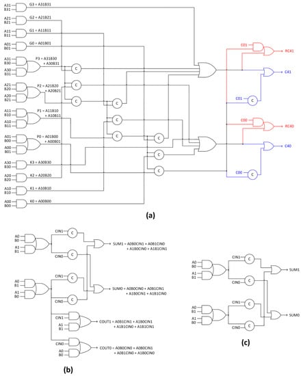
Figure 7.
(a) Proposed 4-bit block carry lookahead generator without redundant carry output (BCLG)/block carry lookahead adder with redundant carry logic (BCLARC); (b) early output full adder; (c) early output sum logic—all corresponding to the 4-phase RTZ handshaking.
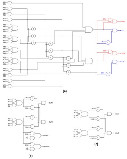
Figure 8.
(a) Proposed 4-bit BCLG/BCLGRC; (b) early output full adder; (c) early output sum logic—all corresponding to the 4-phase RTO handshaking.
The logic equations governing the dual-rail 4-bit lookahead carry output, corresponding to the RTZ handshaking, are given by (3) and (4), where C41 and C40 represent the 4-bit regular dual-rail lookahead carry output. The logical equations for the redundant 4-bit lookahead carry outputs viz. RC41 and RC40 are the same as (3) and (4) although the physical realization of (RC41, RC40) is different from (C41, C40) in the last logic level. In (3) and (4), P0 to P3 represent the carry-propagate signals, G0 to G3 represent the carry-generate signals, and K0 to K3 represent the carry-kill signals. The logic equations for the carry generate, propagate and kill signals are given in Figure 7a, corresponding to the RTZ handshaking. Equations (3) and (4) are inherently in the disjoint sum-of-products form [24], thus satisfying the MCC [10]. In a disjoint sum-of-products, the product terms are mutually orthogonal and the logical conjunction of any two products would yield 0.
C41 = G3 + P3G2 + P3P2G1 + P3P2P1G0 + P3P2P1P0C01
C40 = K3 + P3K2 + P3P2K1 + P3P2P1K0 + P3P2P1P0C00
The proposed early output 4-bit BCLG producing regular lookahead carry outputs, and the 4-bit BCLGRC producing regular and redundant lookahead carry outputs are portrayed in the same figure viz. Figure 7a, which corresponds to the RTZ handshaking. In Figure 7a, the logic highlighted in blue corresponds to the regular carry output (C41, C40) and the logic highlighted in red corresponds to the redundant carry output (RC41, RC40). In the absence of the logic highlighted in red, Figure 7a showcases the 4-bit BCLG used as a building block in Figure 6a,c,d, and in the presence of the logic highlighted in red, Figure 7a showcases the 4-bit BCLGRC used as a building block in Figure 6c,d.
The early output full adder and the sum logic based on [35], which adhere to the RTZ handshaking, are shown in Figure 7b,c respectively along with the corresponding expressions for the sum and carry outputs. (A1, A0), (B1, B0) and (CIN1, CIN0) represent the dual-rail encoded augend, addend and carry inputs of the full adder, and (SUM1, SUM0) and (COUT1, COUT0) represent the corresponding dual-rail encoded sum and carry outputs in Figure 7b and Figure 8b. The physical realization of the sum logic in Figure 7c and Figure 8c is identical to the full adder shown in Figure 7b and Figure 8b, except for the dual-rail encoded carry output. Figure 8a–c are the logical counterparts of Figure 7a–c, which correspond to the RTO handshaking.
The logic rules for transforming an asynchronous design conforming to the RTZ handshaking into a design conforming to the RTO handshaking and vice-versa are given in [44] along with the proofs, and an interested reader may refer to the same for details. The AND, OR, AO21 and AO22 gates in Figure 7 are replaced by their respective duals viz. OR, AND, OA21 and OA22 gates in Figure 8 to adhere to the RTO handshaking but their corresponding inputs are maintained the same. The C-elements in Figure 7 are retained in Figure 8 with the corresponding inputs. In Figure 8a, the logic highlighted in blue specifies the regular carry output (C41, C40), and the logic highlighted in red specifies the redundant carry output (RC41, RC40). In the absence of the logic highlighted in red, Figure 8a is interpreted as the 4-bit BCLG, used in Figure 6a,c,d, and in the presence of the logic highlighted in red, Figure 8a is interpreted as the 4-bit BCLGRC, used in Figure 6c,d.
5. Implementation Results
Twenty-two 32-bit asynchronous adders viz. RCAs, CSLAs, BCLAs, RCLAs, BCLARCs and hybrid BCLARC-RCAs were implemented using a 32/28 nm CMOS process [45]. The adders were treated as an asynchronous circuit stage, as in Figure 1. The adders were realized based on both RTZ and RTO handshaking. The appropriate gates in the standard digital cell library [45], and the 2-input C-element, which was custom implemented as it is not available in the library, were used to realize the asynchronous adders. The input and output registers and the completion detectors were kept respectively identical for the asynchronous adders corresponding to the RTZ and RTO handshaking. Given this, the diverse asynchronous adders differ only in their logic. Hence the differences between their design metrics are due to the differences between their logic compositions.
About a thousand input vectors corresponding to RTZ and RTO handshaking were separately generated and were identically supplied to all the asynchronous adders at time intervals of 20 ns, corresponding to the two handshake protocols, to simulate their functionalities and capture their respective switching activity. Using the switching activity data, the average power dissipation was estimated. Forward latency is akin to critical path delay and is directly estimated. The reverse latency was evaluated based on the timing information pertaining to the gate-level simulations. Area occupancy, worst-case forward and reverse latencies, the maximum cycle time, and the average power dissipation were estimated using Synopsys tools and they are given in Table 1 and Table 2.

Table 1.
Design metrics of various quasi-delay-insensitive (QDI) asynchronous adders (of size 32-bits) estimated using a 32/28 nm bulk CMOS process, corresponding to the 4-phase RTZ handshaking.
Table 2.
Design metrics of various QDI asynchronous adders (of size 32-bits) estimated using a 32/28nm CMOS process, corresponding to the 4-phase RTO handshaking.
The results given in Table 1 correspond to the RTZ handshaking and the results given in Table 2 correspond to the RTO handshaking. These were obtained by targeting a typical case specification of the digital cell library [45] with a supply voltage of 1.05 V and an operating junction temperature of 25 °C. The optimum values of design metrics are highlighted in bold-face in Table 1 and Table 2. Legends ZA1 to ZA22 are used to refer to the adders given in Table 1 which conform to the RTZ handshaking, and legends OA1 to OA22 are used to refer to those adders given in Table 2 which adhere to the RTO handshaking. The adders are arranged in Table 1 and Table 2 randomly i.e., not arranged according to their year of appearance in the literature but are grouped according to their architectural type.
6. Discussion
Some general observations can be made from Table 1 and Table 2 as the trends in the design metrics noticeable in the case of Table 1 are mirrored in Table 2. Adder architectures such as the CSLA and the CLA pave the way for better reduction in the forward latency compared to the RCA architecture, with the CLA architecture more effectively reducing the forward latency compared to the CSLA architecture. However, the RCA architecture enables less reverse latency than the CSLA and CLA architectures. The RCA architecture, depending upon the type of full adder used for the realization, may require less area than the CSLA or CLA architectures. For examples, ZA8 in Table 1 and OA8 in Table 2 require the least area among the various asynchronous adders listed. Even in a synchronous design, the RCA generally consumes less area than any other adder architecture [47]. Despite the difference in the handshaking convention, which would give rise to differences in the kind of logic gates used for the realization, ZA8 and OA8 occupy the same area as given in Table 1 and Table 2. This is because many dual gate pairs in the standard digital cell library [45] have the same area, which may not be the case with commercial digital standard cell libraries. For examples, the minimum size 2-input AND and OR gates in [45] have the same area of 2.03 µm2, the minimum size AO21 and OA21 complex gates have the same area of 2.54 µm2, and the minimum size AO222 and OA222 complex gates have the same area of 3.3 µm2. As a result, it may be inferred that the percentage reductions in the design metrics achieved in the case of the RTO handshaking compared to the RTZ handshaking here tends to serve as a baseline. If a commercial standard digital cell library is considered for the implementations, then the percentage savings in the design metrics for the RTO handshaking over the RTZ handshaking are likely to be higher than what are reported in this work.
Although the latencies and cycle time (and area occupancy) may vary significantly across the asynchronous adders corresponding to one architecture, the average power dissipation does not vary much. For example, the cycle time of ZA1, as seen in Table 1, is 7.9× compared to ZA8 and ZA1 occupies 52.5% more area than ZA8 but the power dissipated by ZA1 is just 1.3% greater than the power dissipation of ZA8. This is because the logic underlying all the asynchronous adders mentioned in Table 1 and Table 2 satisfy the MCC. Therefore, unique signal paths would be activated from the primary inputs up to the primary outputs after the application of input data in all the asynchronous adders. As a result, their average power dissipation tends to be quite close, and indeed close when considering the adders belonging to a specific architecture. Overall, the RTO handshaking is found to be better than the RTZ handshaking as the former enables reduced design metrics than the latter across all the adder architectures, vindicating the observation made in [44]. However, [44] only considered the forward latency, area, and average power dissipation of the existing asynchronous adders for a comparative evaluation based on RTZ and RTO handshaking; the reverse latency, cycle time, and PCTP metrics were neither considered nor provided.
The cycle time is the primary timing parameter of interest in an asynchronous design featuring delay-insensitive data encoding and adhering to a 4-phase handshaking (RTZ/RTO) as the cycle time determines the speed of operation, i.e., the rate at which new data can be input. It may be noted from Table 1 and Table 2 that the BCLARCs feature substantially reduced latencies and cycle time compared to the BCLAs without any redundant carry outputs. It has been shown in [39] that ZA11 achieves better reductions in the design metrics compared to the BCLAs based on [23,32]. This is because the BCLAs pertaining to [23,32] require more logic gates, involve more logic depth, and so exhibit excesses in the design metrics as mentioned in [39]. ZA12 is shown to achieve more optimizations in the design metrics compared to ZA11 of [39]. ZA14, based on [28,39] in Table 1, achieves slightly more optimizations in the design metrics than ZA12, and ZA17 described in [40] achieved by far the maximum optimizations in the design metrics in comparison with other BCLAs, BCLARCs and RCLA. The proposed BCLARC, identified as ZA19 in Table 1 achieves further reductions in all the design metrics compared to ZA17, thus representing the best of the BCLARCs. Suffice to state that all these observations hold well with respect to RTO handshaking. In the case of the CSLA, it is shown in [37] that the asynchronous CSLA based on a uniform 8-8-8-8 input partition (ZA9) resulted in optimum latency, area and power dissipation compared to the other asynchronous CSLAs with respect to the RTZ handshaking. This is found to be also true in the case of the RTO handshaking in this work, where OA9 has reduced design metrics than OA10.
ZA19 in Table 1 and OA19 in Table 2 report the least cycle time among the BCLAs, BCLARCs, CSLAs and RCAs listed corresponding to RTZ and RTO handshaking. Hence, hybrid versions of the proposed BCLARCs (ZA19 and OA19) i.e., BCLARC-RCAs were implemented by utilizing a 4-bit RCA (ZA20 and OA20), an 8-bit RCA (ZA21 and OA21), and a 12-bit RCA (ZA22 and OA22) in the least significant adder bit positions. These hybrid BCLARC-RCAs are specified as BCLARC-RCA1, BCLARC-RCA2 and BCLARC-RCA3 in Table 1 and Table 2. The RCAs introduced serve as a replacement for one, two and three instances of the 4-bit BCLARCs; the example portrayed by Figure 6c depicts the BCLARC-RCA1. The RCAs in ZA20 to ZA22 use the early output full adder of [35] conforming to the RTZ handshaking, and the RCAs in OA20 to OA22 use the same full adder but conforming to the RTO handshaking.
From Table 1 it may be noted that ZA20 and ZA21 achieve reductions in the cycle time and the other design metrics compared to ZA19 but ZA22 has more cycle time than ZA19. As the size of the least significant RCA is increased in a hybrid BCLARC-RCA, beyond a certain limit, the forward latency of the hybrid BCLARC-RCA would increase since the serial cascading of many full adders beyond a certain limit would negatively impact the cycle time. This is found to be true for RTZ handshaking as well, where OA20 and OA21 feature reductions in the design metrics than OA19 but OA22 reports an increase in the cycle time compared to OA19. The proposed hybrid BCLARC-RCA (ZA20) has the minimum cycle time in Table 1 with respect to the RTZ handshaking, and the proposed hybrid BCLARC-RCA (OA20) has the minimum cycle time in Table 2 with respect to the RTO handshaking.
In synchronous designs, the power-delay product (PDP) is often used as a qualitative metric for low power. For evaluating the PDP, the average power dissipation and the critical path delay are considered. In asynchronous designs, the cycle time is the equivalent of the critical path delay of synchronous designs. Therefore, the power-cycle time product (PCTP) is used as a qualitative low power metric. Since the average power dissipation and the cycle time are desirable to be minimized the least value of PCTP is indicative of the best design. The PCTPs of all the asynchronous adders given in Table 1 are computed and then the actual PCTP values are divided by the highest PCTP value to perform a normalization. The same procedure was followed in the case of Table 2.
Figure 9a,b show the plots of the normalized PCTPs of the asynchronous adders listed in Table 1 and Table 2 respectively. The white drop lines in the plots signify the respective normalized PCTP values of the asynchronous adders. The value of ‘1’ represents the highest PCTP value, and the lesser values of PCTP suggest low power designs. Figure 9c shows a one-to-one mapping between the PCTPs of the asynchronous adders corresponding to the RTZ and RTO handshaking after normalization. To perform the normalization for Figure 9c, the actual PCTPs of an asynchronous adder corresponding to the RTZ and RTO handshaking were calculated and the higher of the two PCTPs was used to divide the original PCTPs of both the adders. From Figure 9c, it is seen that the RTO handshaking enables reduced PCTP than the RTZ handshaking for the physical realization of asynchronous adders.
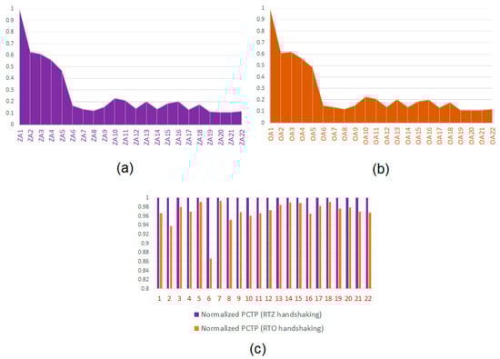
Figure 9.
(a) Normalized power-cycle time products (PCTPs) of the asynchronous adders corresponding to RTZ handshaking; (b) normalized PCTPs of the asynchronous adders corresponding to RTO handshaking; (c) portraying a one-to-one mapping of normalized PCTPs of asynchronous adders (labelled as 1 to 22) with respect to RTZ and RTO handshaking.
On the basis of the RTZ handshaking, the proposed BCLARC (ZA19) achieves the following optimizations in cycle time and PCTP compared to the optimum RCA, CSLA and BCLARC given in Table 1: (i) 14.8% reduction in the cycle time and 14.9% reduction in PCTP compared to the BCLARC (ZA17), (ii) 22.1% reduction in the cycle time and 26% reduction in PCTP compared to the uniform CSLA (ZA9), and (iii) 8.6% reduction in the cycle time and 8% reduction in PCTP compared to the RCA (ZA8). On top of this, notably, the proposed hybrid BCLARC-RCA (ZA20) achieves a 2.4% reduction in the cycle time and an equal reduction in the PCTP compared to the proposed BCLARC (ZA19), which makes the former (ZA20) the best among the adders in Table 1. When comparing ZA20 with the relative timed 32-bit RCA [36] incorporating the latency optimized early output full adder corresponding to the RTZ handshaking, it is noted that ZA20 enables a 4.3% reduction in the cycle time and a 4.1% reduction in the PCTP compared to the latter. The latter is not included in Table 1 since it is not QDI and so non-robust since it incorporates a relative timing assumption of 0.49 ns and the reverse latency being 0.55 ns. If the relative timing assumption exceeds the reverse latency due to any timing variation of some internal gate associated with the carry output logic, then the robustness of the relative timed RCA [36] would be compromised.
For a similar comparison but based on the RTO handshaking, the proposed BCLARC (OA19) achieves the following optimizations in cycle time and PCTP compared to the optimum RCA, CSLA and BCLARC given in Table 1: (i) 15.3% reduction in the cycle time and 15.5% reduction in PCTP compared to the BCLARC (OA17), (ii) 21.5% reduction in the cycle time and 25.5% reduction in PCTP compared to the uniform CSLA (OA9), and (iii) 6.2% reduction in the cycle time and 5.7% reduction in PCTP compared to the RCA (OA8). On top of this, notably, the proposed hybrid BCLARC-RCA (OA20) achieves a 2.1% reduction in the cycle time and a 2.2% reduction in the PCTP compared to the proposed BCLARC (OA19), which makes the former (OA20) the best among the adders in Table 2. When comparing OA20 with the relative timed 32-bit RCA [36], incorporating the latency optimized early output full adder corresponding to the RTO handshaking, it is noted that the former enables a 1.8% reduction in the cycle time and a 1.7% reduction in the PCTP compared to the latter. The latter is not included in Table 2 since it is not QDI and so non-robust since it incorporates a relative timing assumption of 0.49 ns and the reverse latency being 0.55 ns. Again, if the relative timing assumption would exceed the reverse latency due to any timing variation of some internal gate associated with the carry output logic then the robustness of the relative timed RCA [36] would be compromised.
7. Conclusions
This paper described new designs of robust asynchronous early output BCLA (ZA18 and OA18), BCLARC (ZA19 and OA19) and its hybrid variant, the BCLARC-RCA (ZA20 and OA20) corresponding to RTZ and RTO handshaking. The novelty concerns the design of the BCLGRC with respect to RTZ and RTO handshaking (i.e., Figure 7a and Figure 8a). Among the proposed adders, the hybrid BCLARC-RCA (ZA20 and OA20) is found to be optimum from the perspectives of cycle time and PCTP. The proposed hybrid BCLARC-RCA is found to outperform the existing optimum robust asynchronous adders pertaining to RCA, CSLA, and CLA architectures in terms of the cycle time and the PCTP. Further, it is noted that the RTO handshaking is preferable to the RTZ handshaking. For example, the proposed hybrid BCLARC-RCA corresponding to the RTO handshaking (OA20) requires 1.8% less cycle time and achieves a 2.1% reduction in the PCTP than the proposed hybrid BCLARC-RCA corresponding to the RTZ handshaking (ZA20) without any increase in the area occupancy. Hence, the proposed hybrid BCLARC-RCA is a good candidate for the low power asynchronous realization of computer arithmetic by utilizing the RTO handshaking.
Author Contributions
Conceptualization, P.B.; Methodology, P.B., N.M.; Validation, P.B.; Formal Analysis, P.B., D.M., N.M.; Investigation, P.B.; Resources, D.M.; Data Curation, P.B.; Writing-Original Draft Preparation, P.B.; Visualization, P.B.; Supervision, D.M., N.M.; Project Administration, D.M.; Funding Acquisition, D.M.
Funding
This research was funded by the Academic Research Fund (AcRF) Tier-2 research award of the Ministry of Education (MOE), Singapore grant number MOE2017-T2-1-002 and by the AcRF Tier-1 research award of MOE, Singapore grant number RG132/16.
Conflicts of Interest
The authors declare no conflict of interest. The funders had no role in the design of the study; in the collection, analyses, or interpretation of data; in the writing of the manuscript, and in the decision to publish the results.
References
- ITRS. Available online: http://www.itrs2.net (accessed on 1 October 2017).
- Kundu, S.; Sreedhar, A. Nanoscale CMOS VLSI Circuits: Design for Manufacturability; McGraw-Hill: New York, NY, USA, 2010; pp. 1–18. ISBN 978-0071635196. [Google Scholar]
- Nassif, S.R. Modeling and forecasting of manufacturing variations. In Proceedings of the Asia and South Pacific Design Automation Conference, Yokohama, Japan, 2 February 2001. [Google Scholar]
- SElf-Timed DATapath SynthEsis (SEDATE). Available online: http://apt.cs.manchester.ac.uk/projects/sedate/Sedate-AdvertCfS.pdf (accessed on 1 March 2018).
- Van Berkel, C.H.; Josephs, M.B.; Nowick, S.M. Applications of asynchronous circuits. Proc. IEEE 1999, 87, 223–233. [Google Scholar] [CrossRef]
- Tang, B.Z.; Lane, F. Low power QDI asynchronous FFT. In Proceedings of the 22nd IEEE International Symposium on Asynchronous Circuits and Systems, Porto Alegre, Brazil, 8–11 May 2016. [Google Scholar]
- Chang, K.-L.; Chang, J.S.; Gwee, B.-H.; Chong, K.-S. Synchronous-logic and asynchronous-logic 8051 microcontroller cores for realizing the internet of things: A comparative study on dynamic voltage scaling and variation effects. IEEE J. Emerg. Sel. Top. Circuits Syst. 2013, 3, 23–34. [Google Scholar] [CrossRef]
- Martin, A.J.; Nystrom, M. Asynchronous techniques for system-on-chip design. Proc. IEEE 2006, 94, 1089–1120. [Google Scholar] [CrossRef]
- Muller, D.E.; Bartky, S. A theory of asynchronous circuits. In Proceedings of the an International Symposium on the Theory of Switching (Part I), Cambridge, MA, USA, 2–5 April 1957. [Google Scholar]
- Sparsø, J.; Furber, S.B. Principles of Asynchronous Circuit Design: A Systems Perspective; Kluwer Academic Publishers: Dordrecht, The Netherlands, 2001; pp. 9–28. ISBN 978-0792376132. [Google Scholar]
- Moreira, M.T.; Guazzelli, R.A.; Calazans, N.L.V. Return-to-one protocol for reducing static power in C-elements of QDI circuits employing m-of-n codes. In Proceedings of the 25th Symposium on Integrated Circuits and Systems Design, Brasilia, Brazil, 30 August–2 September 2012. [Google Scholar]
- Verhoeff, T. Delay-insensitive codes – an overview. Distrib. Comput. 1988, 3, 1–8. [Google Scholar] [CrossRef]
- Bose, B. On unordered codes. IEEE Trans. Comput. 1991, 40, 125–131. [Google Scholar] [CrossRef]
- Seitz, C.L. System Timing. In Introduction to VLSI Systems; Mead, C., Conway, L., Eds.; Addison-Wesley: Reading, MA, USA, 1980; pp. 218–262. ISBN 978-0201043587. [Google Scholar]
- Balasubramanian, P.; Edwards, D.A. Efficient realization of strongly indicating function blocks. In Proceedings of the IEEE Computer Society Annual Symposium on VLSI, Montpellier, France, 7–9 April 2008. [Google Scholar]
- Balasubramanian, P.; Edwards, D.A. A new design technique for weakly indicating function blocks. In Proceedings of the 11th IEEE Workshop on Design and Diagnostics of Electronic Circuits and Systems, Bratislava, Slovakia, 16–18 April 2008. [Google Scholar]
- Brej, C.F.; Garside, J.D. Early output logic using anti-tokens. In Proceedings of the 12th International Workshop on Logic and Synthesis, Laguna Beach, CA, USA, 28–30 May 2008. [Google Scholar]
- Stevens, K.S.; Ginosar, R.; Rotem, S. Relative timing. IEEE Trans. Very Large Scale Integr. (VLSI) Syst. 2003, 11, 129–140. [Google Scholar] [CrossRef]
- Martin, A.J. The limitation to delay-insensitivity in asynchronous circuits. In Beauty is our Business (Texts and Monographs in Computer Science); Feijen, W.H.J., van Gasteren, A.J.M., Gries, D., Misra, J., Eds.; Springer: New York, NY, USA, 1990; pp. 302–311. ISBN 978-1461287926. [Google Scholar]
- Martin, A.J.; Prakash, P. Asynchronous nano-electronics: preliminary investigation. In Proceedings of the 14th IEEE International Symposium on Asynchronous Circuits and Systems, Newcastle upon Tyne, UK, 7–11 April 2008. [Google Scholar]
- Bi, Y.; Gaillardon, P.-E.; Hu, X.S.; Niemier, M.; Yuan, J.-S.; Jin, Y. Leveraging emerging technology for hardware security–case study on silicon nanowire FETs and graphene SymFETs. In Proceedings of the 23rd IEEE Asian Test Symposium, Hangzhou, China, 16–19 November 2014. [Google Scholar]
- Bi, Y.; Shamsi, K.; Yuan, J.-S.; Gaillardon, P.-E.; De Micheli, G.; Yin, X.; Hu, X.S.; Niemier, M.; Jin, Y. Emerging technology-based design of primitives for hardware security. ACM J. Emerg. Technol. Comput. Syst. 2016, 13, 1–19. [Google Scholar] [CrossRef]
- Sparsø, J.; Staunstrup, J. Delay-insensitive multi-ring structures. Integration 1993, 15, 313–340. [Google Scholar] [CrossRef]
- Balasubramanian, P.; Arisaka, R.; Arabnia, H.R. RB_DSOP: A rule based disjoint sum of products synthesis method. In Proceedings of the 12th International Conference on Computer Design, Las Vegas, NV, USA, 16–19 July 2012. [Google Scholar]
- Varshavsky, V.I. Aperiodic Circuits. In Self-Timed Control of Concurrent Processes: The Design of Aperiodic Logical Circuits in Computers and Discrete Systems; Varshavsky, V.I., Ed.; Translated from the Russian by Yakovlev, A.V.; Kluwer Academic Publishers: New York, NY, USA, 1990; pp. 77–85. ISBN 978-9401067058. [Google Scholar]
- Jeong, C.; Nowick, S.M. Block level relaxation for timing-robust asynchronous circuits based on eager evaluation. In Proceedings of the 14th IEEE International Symposium on Asynchronous Circuits and Systems, Newcastle upon Tyne, UK, 7–10 April 2008. [Google Scholar]
- Brej, C. Early Output Logic and Anti-Tokens. Ph.D. Thesis, The University of Manchester, Manchester, UK, 2006. [Google Scholar]
- Balasubramanian, P. A latency optimized biased implementation style weak-indication self-timed full adder. Facta Univ. Ser. Electron. Energ. 2015, 28, 657–671. [Google Scholar] [CrossRef]
- Toms, W.B. Synthesis of Quasi-Delay-Insensitive Datapath Circuits. Ph.D. Thesis, The University of Manchester, Manchester, UK, 2006. [Google Scholar]
- Balasubramanian, P.; Mastorakis, N.E. QDI decomposed DIMS method featuring homogeneous/heterogeneous data encoding. In Recent Advances in Computers, Communications, Applied Social Science and Mathematics; Mastorakis, N., Mladenov, V., Lepadatescu, B., Karimi, H.R., Helmis, C.G., Eds.; WSEAS Press: Athens, Greece, 2011; pp. 93–101. ISBN 978-1618040305. [Google Scholar]
- Toms, W.B.; Edwards, D.A. Indicating combinational logic decomposition. IET Comput. Digit. Tech. 2011, 5, 331–341. [Google Scholar] [CrossRef]
- Toms, W.B.; Edwards, D.A. Efficient synthesis of speed independent combinational logic circuits. In Proceedings of the 10th Asia and South Pacific Design Automation Conference, Shanghai, China, 18–21 January 2005. [Google Scholar]
- Folco, B.; Bregier, V.; Fesquet, L.; Renaudin, M. Technology mapping for area optimized quasi delay insensitive circuits. In Proceedings of the IFIP 13th International Conference on Very Large Scale Integration (VLSI-SoC), Perth, Australia, 17–19 October 2005. [Google Scholar]
- Balasubramanian, P.; Edwards, D.A. A delay efficient robust self-timed full adder. In Proceedings of the 3rd International Design and Test Workshop, Monastir, Tunisia, 20–22 December 2008. [Google Scholar]
- Balasubramanian, P. A robust asynchronous early output full adder. WSEAS Trans. Circuits Syst. 2011, 10, 221–230. [Google Scholar]
- Balasubramanian, P.; Yamashita, S. Area/latency optimized early output asynchronous full adders and relative-timed ripple carry adders. SpringerPlus 2016, 5, 1–26. [Google Scholar] [CrossRef] [PubMed]
- Balasubramanian, P. Asynchronous carry select adders. Eng. Sci. Technol. Int. J. 2017, 20, 1066–1074. [Google Scholar] [CrossRef]
- Balasubramanian, P.; Edwards, D.A. Power, delay and area efficient self-timed multiplexer and demultiplexer designs. In Proceedings of the 4th International Conference on Design and Technology of Integrated Systems in Nanoscale Era, Cairo, Egypt, 6–9 April 2009. [Google Scholar]
- Balasubramanian, P.; Edwards, D.A.; Toms, W.B. Self-timed section-carry based carry lookahead adders and the concept of alias logic. J. Circuits Syst. Comput. 2013, 22, 1350028. [Google Scholar] [CrossRef]
- Balasubramanian, P.; Dang, C.; Maskell, D.L.; Prasad, K. Asynchronous early output section-carry based carry lookahead adder with alias carry logic. In Proceedings of the IEEE 30th International Conference on Microelectronics, Niš, Serbia, 9–11 October 2017. [Google Scholar]
- Balasubramanian, P.; Dhivyaa, D.; Jayakirthika, J.P.; Kaviyarasi, P.; Prasad, K. Low power self-timed carry lookahead adders. In Proceedings of the IEEE 56th International Midwest Symposium on Circuits and Systems, Columbus, OH, USA, 4–7 August 2013. [Google Scholar]
- Omondi, A.R. Computer Arithmetic Systems: Algorithms, Architecture and Implementations; Prentice Hall International (UK) Limited: Hertfordshire, UK, 1994; ISBN 978-0133343014. [Google Scholar]
- Balasubramanian, P.; Edwards, D.A.; Toms, W.B. Redundant logic insertion and latency reduction in self-timed adders. VLSI Des. 2012, 2012, 1–13. [Google Scholar] [CrossRef]
- Balasubramanian, P. Comparative evaluation of quasi-delay-insensitive asynchronous adders corresponding to return-to-zero and return-to-one handshaking. Facta Univ. Ser. Electron. Energ. 2018, 31, 25–39. [Google Scholar] [CrossRef]
- Synopsys SAED_EDK32/28_CORE Databook. 2012. Available online: https://www.synopsys.com/community/university-program/teaching-resources.html (accessed on 10 December 2017).
- Singh, N.P. A Design Methodology for Self-Timed Systems. Master’s Thesis, Massachusetts Institute of Technology, Cambridge, MA, USA, 1981. [Google Scholar]
- Nagendra, C.; Owens, R.M.; Irwin, M.J. Power-delay characteristics of CMOS adders. IEEE Trans. Large Scale Integr. (VLSI) Syst. 1994, 2, 377–381. [Google Scholar] [CrossRef]


© 2018 by the authors. Licensee MDPI, Basel, Switzerland. This article is an open access article distributed under the terms and conditions of the Creative Commons Attribution (CC BY) license (http://creativecommons.org/licenses/by/4.0/).