Article

A Compact On-Chip Ka-Band Bandpass Filter Using Folded Crossed Interdigital Coupling Structure

Department of Electronic Engineering, National Taipei University of Technology, Taipei City 10608, Taiwan
*
Author to whom correspondence should be addressed.
Electronics 2026, 15(7), 1455; https://doi.org/10.3390/electronics15071455
Submission received: 7 March 2026 / Revised: 26 March 2026 / Accepted: 28 March 2026 / Published: 31 March 2026
(This article belongs to the Special Issue New Challenges in Beyond 5G/6G Network Wireless Technologies)

Abstract

This paper proposes a millimeter-wave miniature on-chip bandpass filter (BPF) implemented using a 0.18 μm CMOS process. To address the issues of insufficient coupling capability, limited control of transmission zeros, and excessive chip area in traditional on-chip filters, a folded cross-interdigital coupling structure is proposed to enhance coupling efficiency and reduce size. The design incorporates metal–insulator–metal (MIM) capacitors to increase the coupling capacitance between resonators without increasing the area, and utilizes a defected ground structure (DGS) to modify the current distribution at the ground plane, generating additional transmission zeros to improve selectivity. An LC equivalent circuit model was established and verified through full-wave electromagnetic simulation, and the design was validated through chip fabrication and on-wafer measurements. The measurement results show an insertion loss of 3.36 dB and a fractional bandwidth of 49.1% at 32 GHz, with two transmission zeros. The core dimensions are 0.25 mm × 0.18 mm. This design achieves a good balance between miniaturization, selectivity, and insertion loss, making it suitable for millimeter-wave SoC applications.

1. Introduction

As RF wireless systems continue to move to higher frequencies, wireless communication systems must be able to handle a variety of high-frequency circuit signals [1,2,3]. Demand is increasing for high-frequency circuit devices in the millimeter wave area, which provides a wide range of broadband applications for high-speed wireless communication systems. Bandpass filters are key components, which often require high selectivity and low insertion loss (IL). The requirements for filters are low cost, compact structure, and easy system integration [4,5,6].
The millimeter-wave radio frequency integrated circuit (RFIC) chip presented as a wafer module has attracted considerable attention [7,8]. Implementing passive components together with active circuits on a chip not only improves system integrity, but also avoids the use of complex packaging techniques to increase reliability [9,10]. Among the passive components, the filter is an essential component in the RF front-end circuit, and the bandpass filter is an important basic component in the transmitter and receiver. Therefore, the filter is mainly used to reduce noise and suppress interference signals outside the system. In the technical literature, several studies of bandpass filters have been published, such as filters made by substrate synthesized waveguide (SIW) [11,12,13,14], filters designed with defected ground structure (DGS) [15,16,17] and filters implemented in the complementary metal oxide semiconductor (CMOS) process for microelectromechanical systems (MEMS) technology [18,19]. Based on the aforementioned studies, various filter implementations exhibit inherent trade-offs among performance, size, and integration capability. SIW-based filters typically achieve high quality factor and low insertion loss owing to their waveguide-like characteristics; however, their relatively large footprint limits their suitability for highly integrated RFIC applications. DGS-based designs enhance selectivity and stopband suppression by perturbing current distributions, but at the cost of increased radiation loss and design complexity, particularly at millimeter-wave frequencies. In contrast, CMOS-based and MEMS-integrated filters offer superior compactness and compatibility with system-on-chip integration. Nevertheless, their performance is often constrained by substrate losses and limited passive component quality, leading to reduced quality factor and increased insertion loss. Consequently, the realization of a compact on-chip bandpass filter that simultaneously achieves wide bandwidth, low insertion loss, and high integration compatibility in standard CMOS technology remains a challenging problem. This motivates the development of advanced design methodologies to address these conflicting requirements.
On-chip bandpass filters implemented in CMOS processes typically have low quality factors due to the effects of conductor loss and substrate coupling. In millimeter-wave applications, particularly in wideband designs, the Q-factor is usually below 5, and insertion loss typically falls within the range of 2–5 dB, varying with the degree of miniaturization and process conditions. Current on-chip filters can be broadly categorized into transmission line structures, lumped-element designs, and miniaturized topologies with enhanced coupling. Transmission line filters, while offering higher Q-factors and lower insertion loss, are relatively large in the millimeter-wave band, which hinders high integration. Lumped-element designs can effectively reduce size but are limited by insufficient coupling capability and parasitic effects; enhanced-coupling designs can improve bandwidth and selectivity but are typically accompanied by increased design complexity or loss. In CMOS millimeter-wave design, simultaneously achieving miniaturization, strong coupling, controllable transmission zeros, and reasonable insertion loss remains a key challenge.
Millimeter-wave bandpass filter devices have received particular attention in recent years, but their design requires evaluation of insertion loss, operating bandwidth, band rejection, and die size, making millimeter-wave filter design a major challenge today.
By miniaturizing passive components, it helps to reduce die size, but it also helps to reduce conductor loss and optimize overall insertion loss. Many studies have proposed design methods for miniaturization of lumped elements [20,21,22]. The most important point of this method is to use the metal stack of the wafer to enhance self-coupling. On the design side, in order to reduce the microstrip line distribution and bandpass filter area, metal–insulator–metal (MIM) capacitors are added in the middle of the multimode resonators [23,24] or defected ground structures are used to reduce insertion losses [25,26,27]. The chip filter circuit size is reduced by folding the microstrip resonator [28,29,30]. However, it can also sacrifice insertion loss, return loss, or stopband suppression.
Conventional on-chip filters suffer from insufficient coupling capability, limited control over transmission zeros, and excessive chip area. This study proposes a miniature Ka-band on-chip bandpass filter implemented using a 0.18 μm CMOS process. It employs a folded-cross interdigital structure combined with MIM capacitors to enhance coupling capability while reducing the chip area. Furthermore, a defected ground structure (DGS) is introduced to generate additional transmission zeros and improve selectivity. The design has been verified through LC modeling, electromagnetic simulation, and measurement, achieving a good balance between size, bandwidth, and insertion loss, making it suitable for millimeter-wave SoC applications.

2. Design and Implementation of the Interdigital-Type BPF

2.1. Overview of the BPF

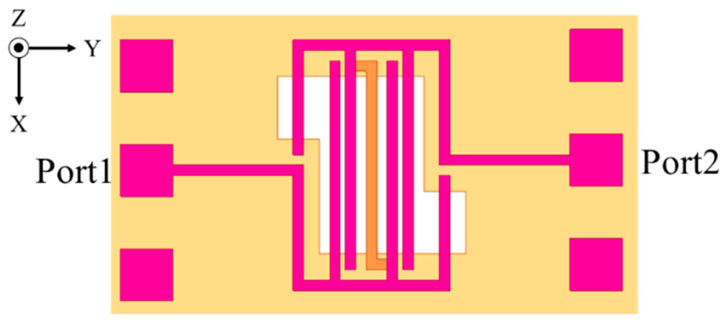
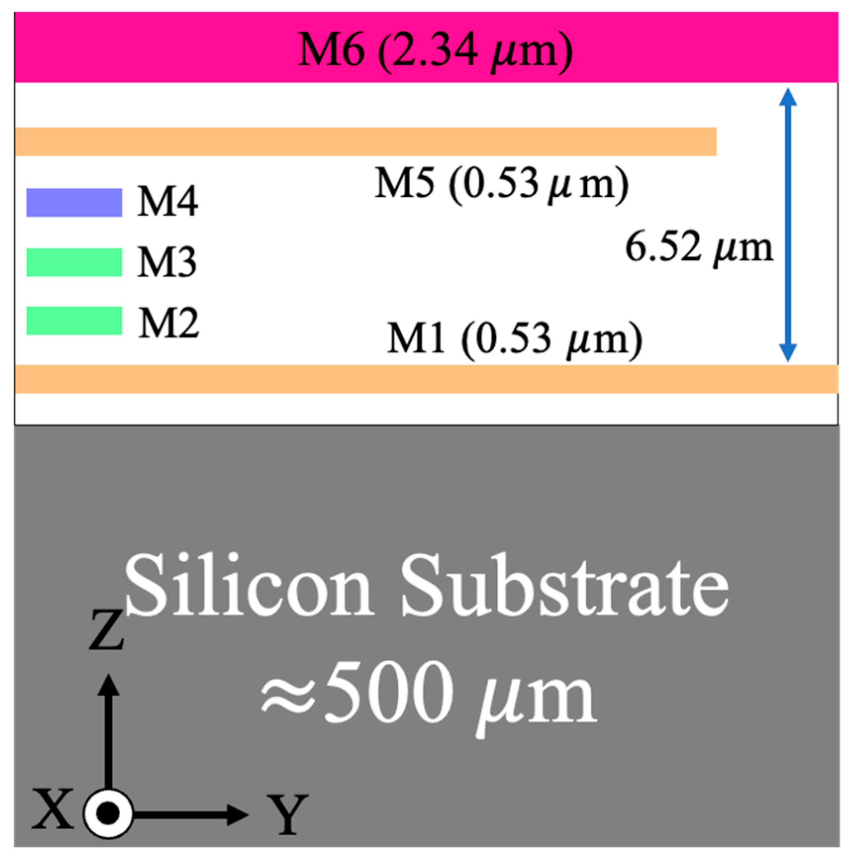
The layout of the proposed chip millimeter wave passive element integrated with the bandpass filter is shown in Figure 1. Figure 2 depicts this design using standard 0.18 μm CMOS technology, providing six metal layers, denoted by M1-M6 from bottom to top. The height of the silicon substrate is 500 μm, the dielectric constant is 11.9, and the dielectric constant of SiO2 is 4.0. The resonator and feeding line of the filter are constructed in M6, which has the largest thickness and has lower conduction loss. The grounding layer is selected at M1, when the maximum height of the substrate between the two layers can reduce the conduction loss. The additional MIM capacitor layer is located between M1 and M5.
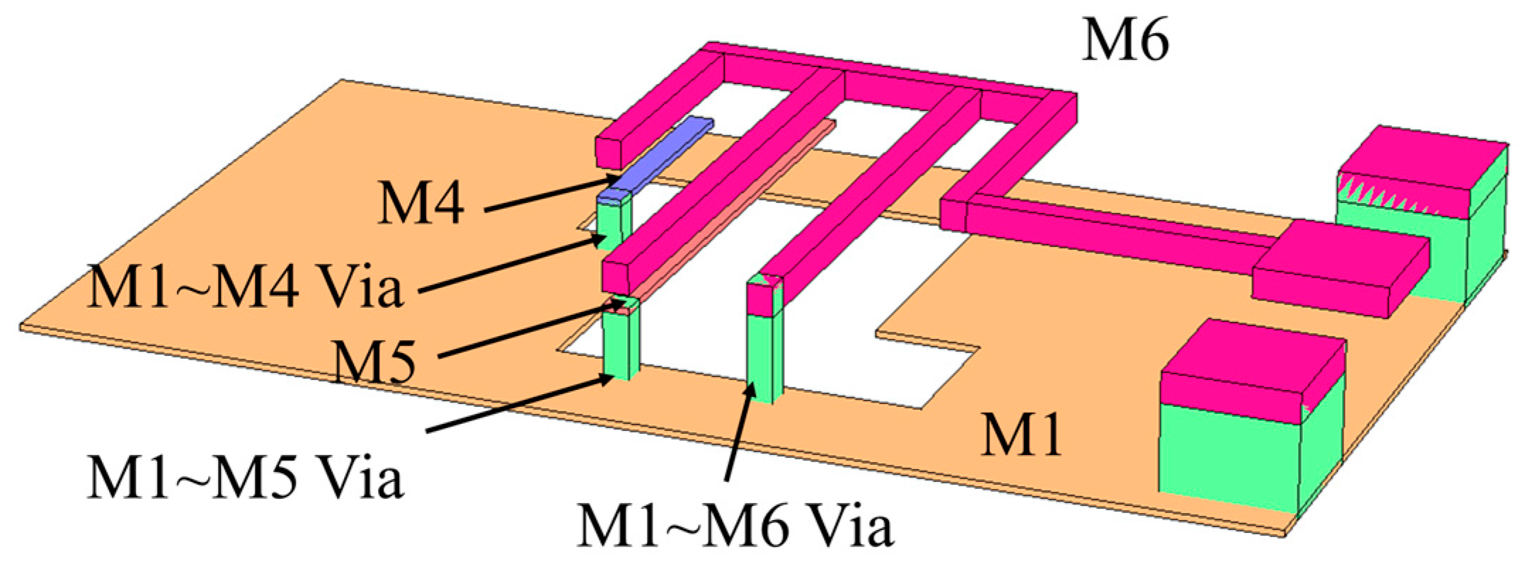
The bandpass filter is composed of crossed interdigital-type resonators, as shown in Figure 3. The folding and overlapping are used to reduce the size. The end and middle branches of the resonator are loaded by MIM capacitors, while the branch near the feed-through end is connected to ground using a through-hole (VIA) from M1 to M6. These layers are connected to the open end of the resonator and to the ground layer through vias. A defected ground structure is etched below the resonator to improve performance.

2.2. LC Equivalent Circuit Model of the BPF

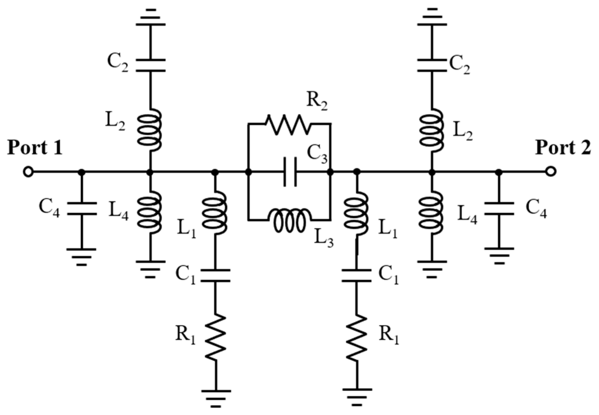
The designed lossless LC equivalent circuit model of RF CMOS Ka-Band bandpass filter is in Figure 4. The LC circuit model consists of four combinations: The first is the series circuit of L 1 , C 1 , and R 1 . The second is the series circuit of L 2 and C 2 . The third is the defected ground structure effect of L 3 , C 3 , and R 1 . And the fourth is the high-frequency coupling of the parallel branch of L 4 and C 4 . Since the transmission zeros (TZs) are able to be adjusted by the defected ground structure, the mathematical formula for the TZs can be derived as in (1).
f T Z = 1 2 π L 3 C 3
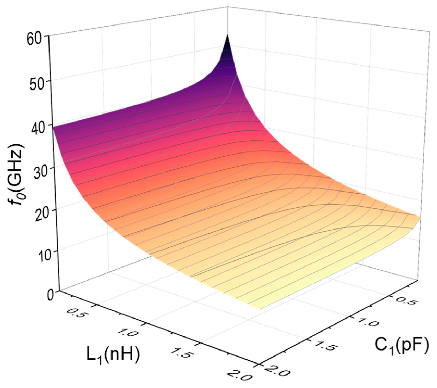
The resonant frequency f 0 of the BPF can be determined by L 1 and C 1 . The relationship between f 0 , L 1 and C 1 can be represented by 3-D mapping as shown in Figure 5. It can be observed that the lower values of f 0 occur at the larger values of L 1 and the larger values of C 1 . Finally, the resonant frequency can be determined by adjusting L 1 and C 1 .
The coupling coefficient k between resonators can be expressed in terms of the resonance frequencies of the even and odd modes as [31]
k = f e v e n 2 f o d d 2 f e v e n 2 + f o d d 2
where f e v e n and f o d d represent the resonance frequencies of the coupled resonators under even-mode and odd-mode excitation conditions, respectively. Even and odd modes correspond to cases where the electric field distributions between the resonators are in phase and out of phase, respectively; the difference in their frequencies reflects the coupling strength between the resonators. Therefore, the coupling coefficient k can be used to quantify the strength of the interaction between the coupled resonators. From a circuit perspective, the coupling coefficient is directly related to the equivalent coupling capacitance between adjacent resonators. By introducing metal–insulator–metal (MIM) capacitors in the overlapping region, the equivalent coupling capacitance can be effectively increased, thereby enhancing the coupling strength between resonators. This effect can be observed in the parametric analysis shown in Figure 5, Figure 6, Figure 7 and Figure 8; changes in capacitance values have a significant impact on the bandwidth and the location of the transmission zero.
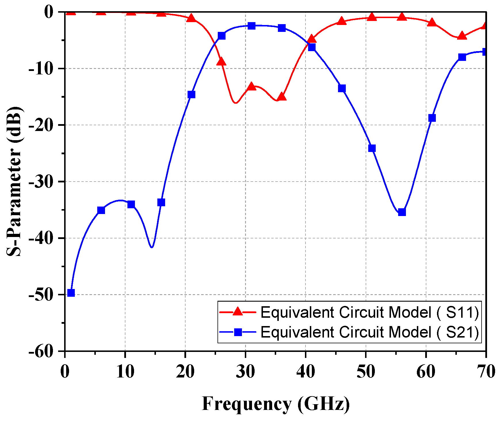
The LC equivalent circuit was then verified by the Advanced Design System (ADS). Figure 6 shows the bandwidth of the Ka-band bandpass filter architecture design with 52.3% fractional bandwidth (FBW) (from 24.8 to 42.4 GHz). The transmission zero of the lower resistance band is at 14.4 GHz, which can suppress the low frequency band by 30 dB. This provides good suppression in the low-orbit satellite band and the sub-6 GHz band.
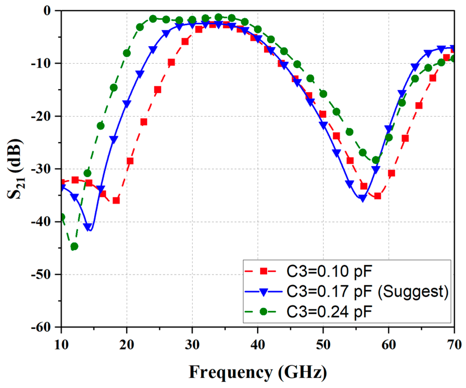
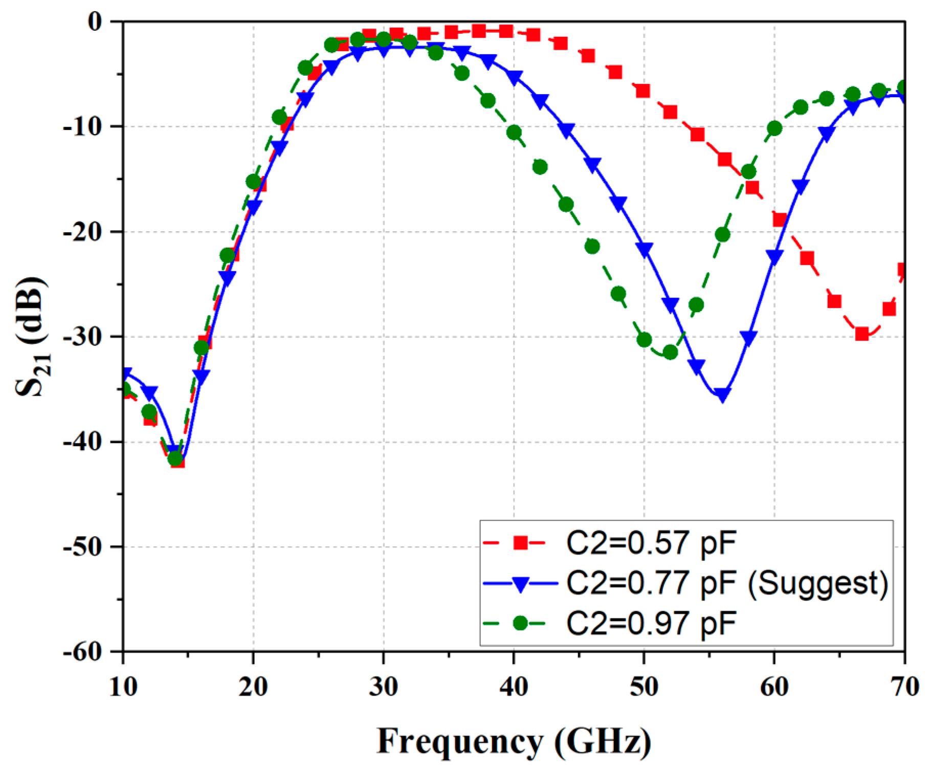
To further analyze the proposed bandpass filter design architecture, the equivalent circuit model is investigated by ADS 2023 for the parameters. The analysis of the transmission zero is performed for the bandpass filter in Figure 7. When L 3 = 0.17 nH and R 1 = 300 ohms, the transmission zero point of the lower resistance band can be adjusted from 15.6 to 13.2 GHz with the value of C 3 from 0.14 to 0.20 pF, while the transmission zero of the upper resistance band is almost unchanged. Therefore, when the value of C 3 becomes larger, the transmission zero point will move to a lower frequency. Similarly, the transmission zero for higher frequencies can be adjusted by L 2 and C 2 . As shown in Figure 8, when L 2 = 0.097 nH, the transmission zero point of the upper band can be adjusted from 51.5 to 66.7 GHz as the value of C 2 changes from 0.057 to 0.097 pF. The transmission zero of the lower band remains unchanged.

2.3. Implementation of the BPF with DGS

The DGS can create a new transmission zero at the edge of the passband and improve performance through additional coupling. This design takes advantage of this additional coupling to improve insertion loss. The DGS improves the magnetic and electrical coupling between the resonators.
Electrical coupling is also improved due to the reduced coupling between the ground plane and the resonator.
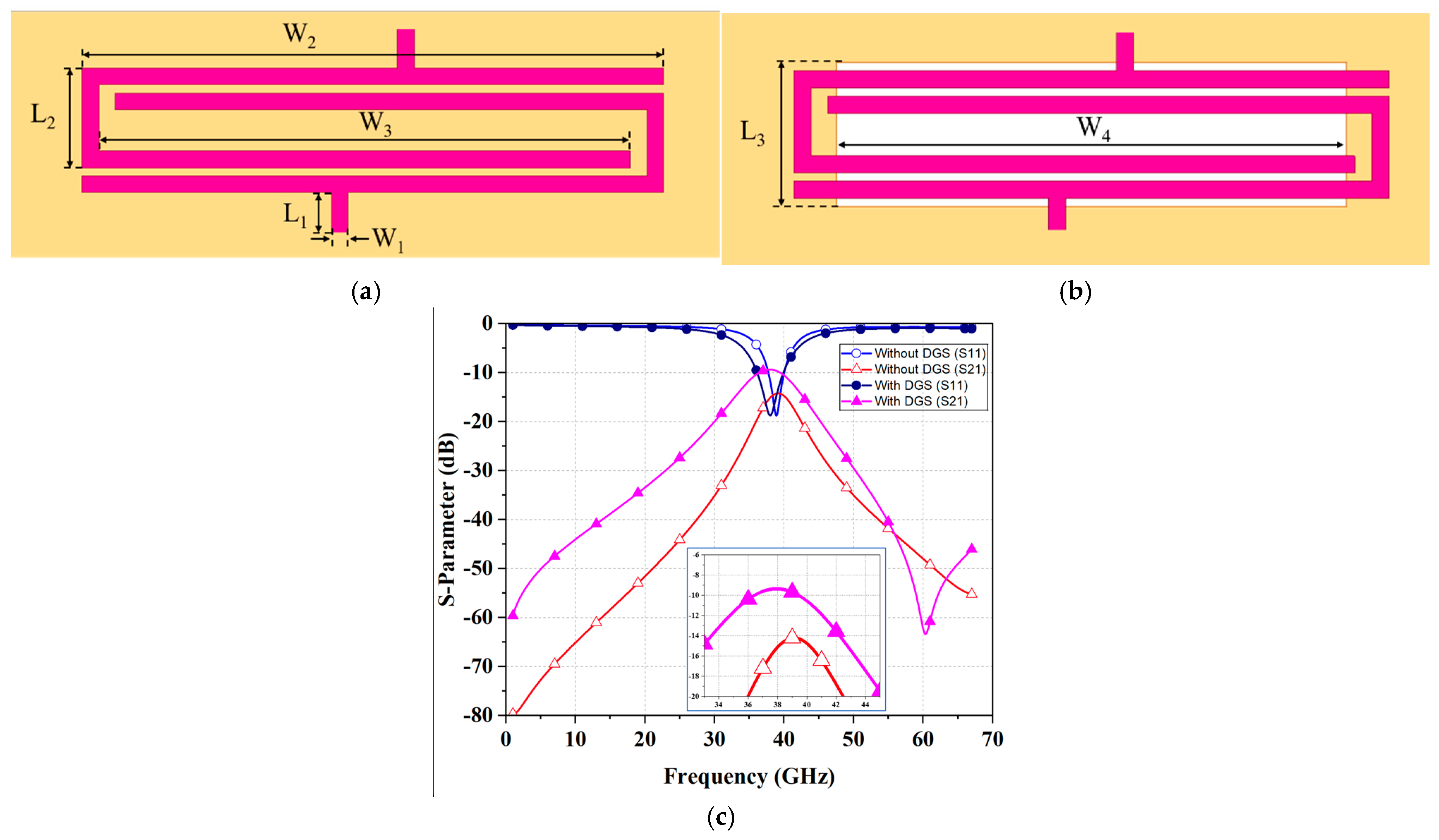
Figure 9a shows the interdigital-type bandpass filter without DGS, and Figure 9b shows the ground structure by introducing a rectangular defect below the coupling resonator. Comparing the effect of the ground structure with and without the defect on the electromagnetic simulation in Figure 9c, the bandpass filter has a similar ratio bandwidth and an improvement from 14 to 9 dB in insertion loss. In addition, due to the variations in the effective capacitance and inductance of the circuit, a new transmission zero point is formed at 60 GHz.
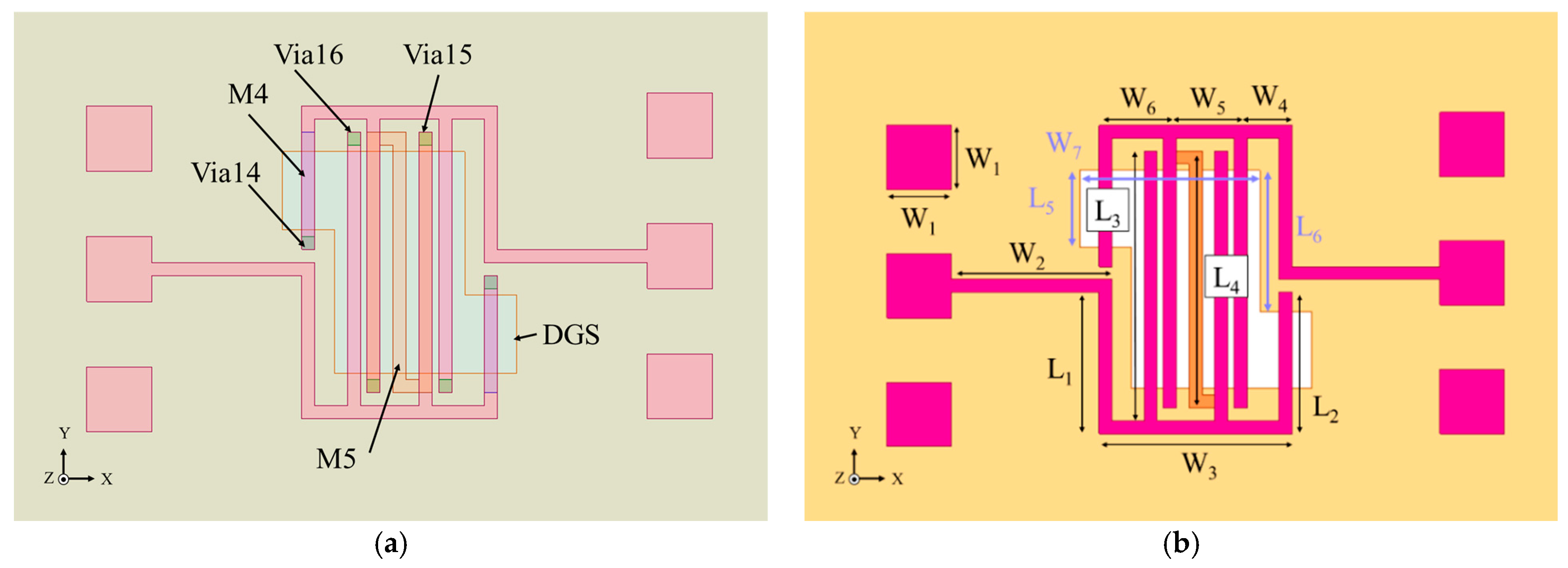
To demonstrate the validity of the filter, the circuit structure model has to be converted into a specific physical layout. The proposed bandpass filter layout is a symmetric structure consisting of feed-in transmission lines, interleaved interdigital-coupled resonators, MIM capacitors, and defected ground. The final proposed design layout of the Ka-band bandpass filter is shown in Figure 10, and the alignment width is unified to 10 μm.
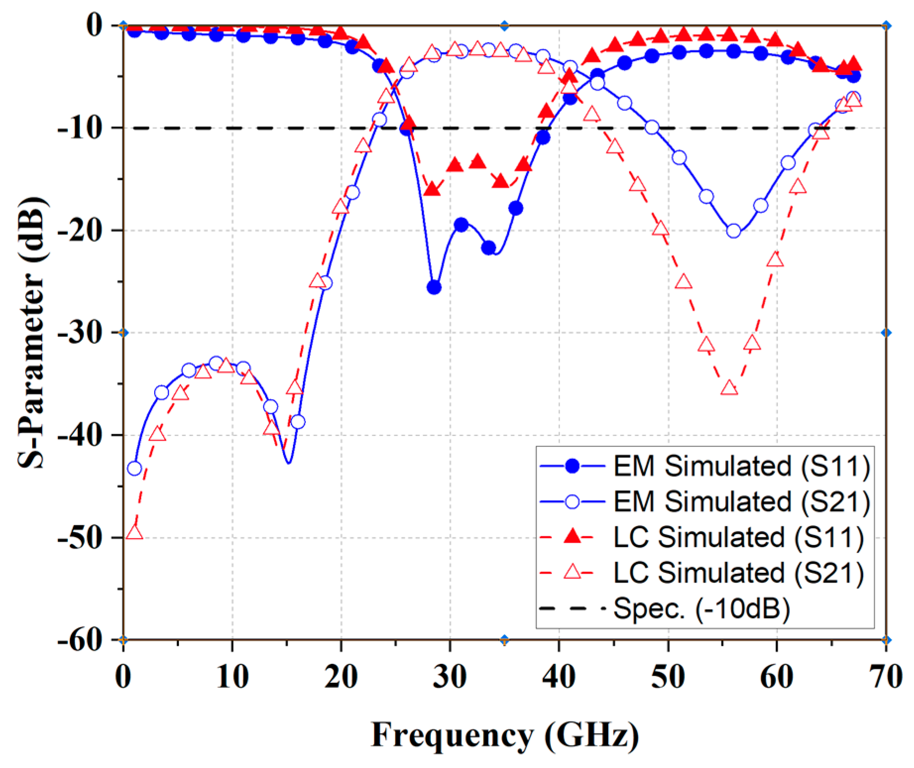
Figure 11 illustrates the bandwidth of the electromagnetic simulation and the LC equivalent circuit simulation for the Ka-band bandpass filter proposed in Figure 4, and it can be seen that the electromagnetic simulation has an FBW of 53.4% from 24.8 to 42.9 GHz, while the transmission zero of the lower resistance band remains the same as the LC equivalent circuit at 14.8 GHz. However, the insertion loss is reduced from 1.47 to 2.69 dB, which is the result of the difference caused by the effect of the silicon substrate, but it does not affect the functionality.

3. Bandpass Filter Fabrication and Measurement Results

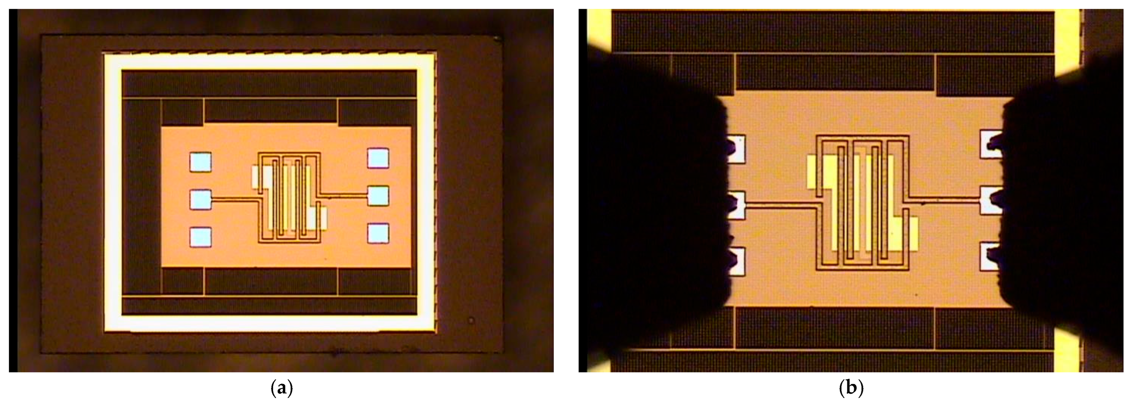
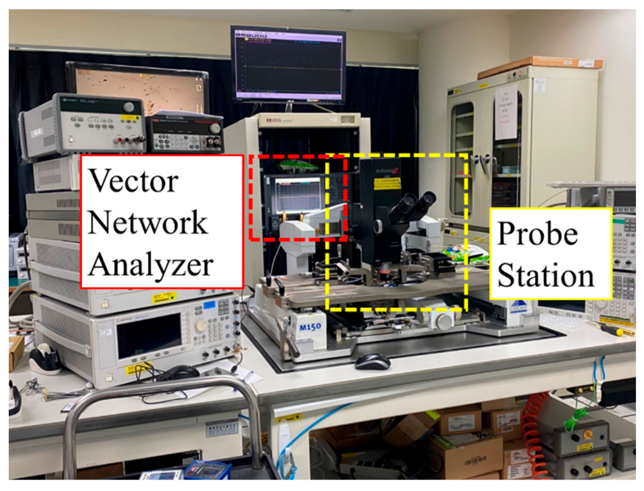
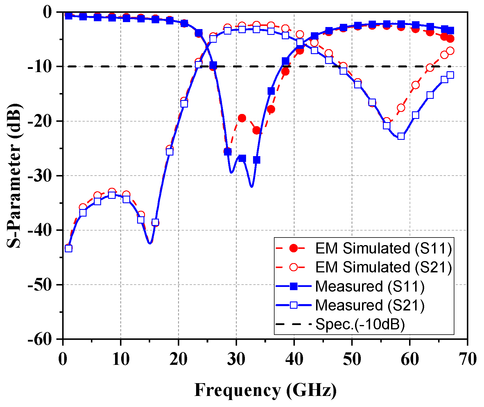
The designed bandpass filter is fabricated with TSMC 0.18 μm CMOS technology. Figure 12a shows the chip of the interleaved interdigital-type bandpass filter with a core size of 0.25 mm × 0.18 mm. If a probe test point is included, the size is 0.28 mm × 0.48 mm. The probe spacing used for measurement is 100 μm. Figure 13 shows the measurement environment using an Agilent E8257D vector network analyzer (Agilent Technologies, Santa Clara, CA, USA), which provides measurements up to 67 GHz, as shown in Figure 14. The electromagnetic simulations and measurements show good agreement. The bandpass filter measured an insertion loss of 3.36 dB at 32 GHz, with a passband band from 25.0 GHz to 41.3 GHz and an FBW of 49.1%. There is a small variation between simulation and measurement, which may be due to probe measurement errors or manufacturing tolerances. The quality factor of this filter is evaluated based on the measured center frequency and bandwidth; with a center frequency of 32 GHz and a bandwidth of 16 GHz, its loaded Q is approximately 2.
The measured S-parameters are not de-embedded and include the effects of probing pads and access interconnections. These parasitic effects may contribute to additional insertion loss, but the impact is limited due to the compact layout.
The performance of the fabricated bandpass filters and several CMOS chip bandpass filters recently proposed in the literature are summarized in Table 1. The proposed design has successfully demonstrated a good balance between compactness, selectivity and in-band insertion loss level. The smaller size achieved by the defected ground structure design is more dimensionally advantageous compared to [10,24,29,32]. In addition, the bandpass filter has lower or equivalent insertion loss compared to [10,23,33]. Due to the lossy silicon substrate and ohm loss, the silicon-based BPF has a higher insertion loss compared to the filter implemented in [34], but the overall size of the proposed bandpass filter is much smaller.

4. Conclusions

A compact interdigital-coupled bandpass filter implemented in 0.18 μm CMOS technology is presented. Interleaved, overlapped and defected ground structures are utilized to produce compact size, small insertion loss and highly selective filter performance. The DGS generates transmission zeros at lower frequencies. Reasonable agreement is obtained between the electromagnetic simulation and measurement results.
The results illustrate that a small insertion loss of 3.36 dB is achieved over 25.0 to 41.3 GHz with a chip size (without probe test points) of only 0.045 mm2. The achieved results demonstrate the possibility of design miniaturization and the proposed aggregate component approach is very suitable for chip bandpass filters.
The performance is mainly affected by substrate loss, process variations, and increased parasitic effects at higher frequencies, which may limit the achievable quality factor and introduce deviations between simulation and measurement. Despite these inherent limitations of CMOS-based millimeter-wave implementations, the proposed design maintains stable filter characteristics and demonstrates its effectiveness for compact on-chip bandpass filter applications.

Author Contributions

Conceptualization, M.-A.C., C.-W.L. and B.-R.C.; methodology, M.-A.C. and C.-W.L.; software, M.-A.C., C.-W.L. and B.-R.C.; validation, M.-A.C., C.-W.L. and B.-R.C.; formal analysis, M.-A.C., C.-W.L. and B.-R.C. investigation, C.-W.L. and B.-R.C. resources, M.-A.C., C.-W.L. and B.-R.C.; writing—original draft preparation, M.-A.C. and B.-R.C.; writing—review and editing, M.-A.C. and C.-W.L.; visualization, M.-A.C.; supervision, M.-A.C.; project administration, M.-A.C.; funding acquisition, M.-A.C. All authors have read and agreed to the published version of the manuscript.

Funding

This research received no external funding.

Institutional Review Board Statement

Not applicable.

Data Availability Statement

All data are included within the manuscript.

Conflicts of Interest

The authors declare no conflicts of interest.

References

  1. Zhu, X.; Gómez-García, R. Exploiting parasitic capacitances in 3-D inductors to design RF CMOS quasi-elliptic-type broad-band bandpass filters. IEEE Trans. Circuits Syst. II Express Briefs 2021, 68, 3128–3132. [Google Scholar] [CrossRef] [Scilit]
  2. Ge, Z.; Chen, L.; Gomez-Garcia, R.; Zhu, X. Millimeter-wave wide-band bandpass filter in CMOS technology using a two-layered highpass-type approach with embedded upper stopband. IEEE Trans. Circuits Syst. II Express Briefs 2021, 68, 1586–1590. [Google Scholar] [CrossRef] [Scilit]
  3. Zhu, H.; Zhu, X.; Yang, Y.; Xue, Q. Design of Wideband Third-Order Bandpass Filters Using Broadside-Coupled Resonators in 0.13-μm (Bi)-CMOS Technology. IEEE Trans. Microw. Theory Tech. 2018, 66, 5593–5604. [Google Scholar] [CrossRef] [Scilit]
  4. Xiu, T.; Yao, Y.; Jiang, H.; Cheng, X.; Wang, C.; Wang, B.; Yu, J.; Chen, X. Design of a Compact and Low-Loss E-Band Filter Based on Multilayer Groove Gap Waveguide. IEEE Microw. Wirel. Compon. Lett. 2021, 31, 1211–1214. [Google Scholar] [CrossRef] [Scilit]
  5. Castro, N.; Pizarro, F.; Herrán-Ontanón, L.F.; Rajo-Iglesias, E. Evaluation of inverted microstrip gap waveguide bandpass filters for Ka-band. AEU-Int. J. Electron. Commun. 2021, 134, 153677. [Google Scholar] [CrossRef] [Scilit]
  6. Bhat, Z.A.; Sheikh, J.A.; Khan, S.D.; Rehman, R.; Ashraf, S. Compact and novel coupled line microstrip bandpass filter based on stepped impedance resonators for millimetre-wave communications. Frequenz 2021, 75, 147–152. [Google Scholar] [CrossRef] [Scilit]
  7. Vanukuru, V.N.R.; Velidi, V.K. Millimeter-wave CMOS 30/80 GHz sharp-rejection dual-band bandstop filters using TFMS open-stepped-Impedance resonators. IEEE Trans. Circuits Syst. II Express Briefs 2020, 68, 201–205. [Google Scholar]
  8. Kim, N.-S. A digital-intensive extended-range dual-mode BLE5. 0 and IEEE802. 15.4 transceiver SoC. IEEE Trans. Microw. Theory Tech. 2020, 68, 2020–2029. [Google Scholar] [CrossRef] [Scilit]
  9. Vanukuru, V.N.R.; Velidi, V.K. CMOS millimeter-wave ultra-wideband bandpass filter with three reflection-zeros using compact single TFMS coupled-line hairpin unit. IEEE Trans. Circuits Syst. II Express Briefs 2019, 67, 77–81. [Google Scholar] [CrossRef] [Scilit]
  10. Li, M.; Yang, Y.; Da Xu, K.; Zhu, X.; Wong, S.W. Microwave on-chip bandpass filter based on hybrid coupling technique. IEEE Trans. Electron Devices 2018, 65, 5453–5459. [Google Scholar] [CrossRef] [Scilit]
  11. Lu, R.; Yu, C.; Wu, F.; Yu, Z.; Zhu, L.; Zhou, J.; Yan, P.; Hong, W. SIW cavity-fed filtennas for 5G millimeter-wave applications. IEEE Trans. Antennas Propag. 2021, 69, 5269–5277. [Google Scholar] [CrossRef] [Scilit]
  12. Qiang, J.; Xu, F.; Yang, L.; Liu, S.; Zhan, J.; Li, M. A high-performance empty substrate integrated waveguide filter with mixed electric and magnetic coupling. Microw. Opt. Technol. Lett. 2022, 64, 707–711. [Google Scholar] [CrossRef] [Scilit]
  13. Chu, P.; Guo, L.; Zhang, L.; Xu, F.; Hong, W.; Wu, K. Wide stopband substrate integrated waveguide filter implemented by orthogonal ports’ offset. IEEE Trans. Microw. Theory Tech. 2020, 68, 964–970. [Google Scholar] [CrossRef] [Scilit]
  14. Feng, Y.; Fang, S.; Jia, S.; Xu, Z. Tri-Layered Stacked Substrate Integrated Waveguide Bandpass Filter Using Non-Resonant Nodes Excitation. IEEE Trans. Circuits Syst. II Express Briefs 2021, 69, 1004–1008. [Google Scholar] [CrossRef] [Scilit]
  15. Rao, Y.; Qian, H.J.; Yang, B.; Gómez-García, R.; Luo, X. Dual-band bandpass filter and filtering power divider with ultra-wide upper stopband using hybrid microstrip/DGS dual-resonance cells. IEEE Access 2020, 8, 23624–23637. [Google Scholar] [CrossRef] [Scilit]
  16. Wei, Z.; Yang, T.; Chi, P.-L.; Zhang, X.; Xu, R. A 10.23–15.7-GHz varactor-tuned microstrip bandpass filter with highly flexible reconfigurability. IEEE Trans. Microw. Theory Tech. 2021, 69, 4499–4509. [Google Scholar] [CrossRef] [Scilit]
  17. Han, Y.-N.; Liu, Z.-H.; Lin, Y.; Cheng, C.-Y.; Zhou, Y.-Y. Dual-Band Bandstop Filtering Cable Design Using Defected Conductor Layer With Asymmetric Spiral Structure. IEEE Trans. Microw. Theory Tech. 2022, 70, 3154–3162. [Google Scholar] [CrossRef] [Scilit]
  18. Asadi, M.J.; Jin, R.; Ding, G.; Hwang, J.C.; Scarbrough, D.; Goldsmith, C.L. CMOS Closed-Loop Control of MEMS Varactors for Robust K a-Band Tunable Filters. J. Microelectromech. Syst. 2019, 28, 910–918. [Google Scholar] [CrossRef] [Scilit]
  19. Yang, Z.; Psychogiou, D.; Peroulis, D. Design and optimization of tunable silicon-integrated evanescent-mode bandpass filters. IEEE Trans. Microw. Theory Tech. 2018, 66, 1790–1803. [Google Scholar] [CrossRef] [Scilit]
  20. Ge, Z.; Chen, L.; Yang, L.; Gómez-García, R.; Zhu, X. On-chip millimeter-wave integrated absorptive bandstop filter in (Bi)-CMOS technology. IEEE Electron Device Lett. 2020, 42, 114–117. [Google Scholar] [CrossRef] [Scilit]
  21. Guo, Y.-J.; Xu, K.-D.; Deng, X.; Cheng, X.; Chen, Q. Millimeter-wave on-chip bandpass filter based on spoof surface plasmon polaritons. IEEE Electron Device Lett. 2020, 41, 1165–1168. [Google Scholar] [CrossRef] [Scilit]
  22. Xu, K.-D.; Guo, Y.-J.; Liu, Y.; Deng, X.; Chen, Q.; Ma, Z. 60-GHz compact dual-mode on-chip bandpass filter using GaAs technology. IEEE Electron Device Lett. 2021, 42, 1120–1123. [Google Scholar] [CrossRef] [Scilit]
  23. Bautista, M.G.; Zhu, H.; Zhu, X.; Yang, Y.; Sun, Y.; Dutkiewicz, E. Compact Millimeter-Wave Bandpass Filters Using Quasi-Lumped Elements in 0.13-μm (Bi)-CMOS Technology for 5G Wireless Systems. IEEE Trans. Microw. Theory Tech. 2019, 67, 3064–3073. [Google Scholar] [CrossRef] [Scilit]
  24. Xu, K.-D.; Zhu, X.; Yang, Y.; Chen, Q. A broadband on-chip bandpass filter using shunt dual-layer meander-line resonators. IEEE Electron Device Lett. 2020, 41, 1617–1620. [Google Scholar] [CrossRef] [Scilit]
  25. Elsaidy, E.; Barakat, A.; Abdel-Rahman, A.B.; Allam, A.; Pokharel, R.K. Ultracompact CMOS 60-GHz tapped-line combline BPF with two transmission zeros using defected ground structures. IEEE Trans. Compon. Packag. Manuf. Technol. 2018, 8, 1642–1649. [Google Scholar] [CrossRef] [Scilit]
  26. Thapa, S.K.; Pokharel, R.K.; Chen, B.; Barakat, A. On-chip Millimeter-Wave DGS based Bandstop Filter in 0.18-μm CMOS Process. IEEE Trans. Circuits Syst. II Express Briefs 2022, 69, 2732–2736. [Google Scholar] [CrossRef] [Scilit]
  27. Abd El-Hameed, A.S.; Barakat, A.; Abdel-Rahman, A.B.; Allam, A.; Pokharel, R.K. Ultracompact 60-GHz CMOS BPF employing broadside-coupled open-loop resonators. IEEE Microw. Wirel. Compon. Lett. 2017, 27, 818–820. [Google Scholar] [CrossRef] [Scilit]
  28. Hou, Z.J.; Yang, Y.; Zhu, X.; Li, Y.C.; Dutkiewicz, E.; Xue, Q. A compact and low-loss bandpass filter using self-coupled folded-line resonator with capacitive feeding technique. IEEE Electron Device Lett. 2018, 39, 1584–1587. [Google Scholar] [CrossRef] [Scilit]
  29. Sun, F.; Zhu, H.; Zhu, X.; Yang, Y.; Sun, Y.; Zhang, X. Design of millimeter-wave bandpass filters with broad bandwidth in Si-based technology. IEEE Trans. Electron Devices 2019, 66, 1174–1181. [Google Scholar] [CrossRef] [Scilit]
  30. Chen, L.; Zhu, H.; Gómez-García, R.; Zhu, X. Miniaturized On-Chip Notch Filter With Sharp Selectivity and> 35-dB Attenuation in 0.13-μm Bulk CMOS Technology. IEEE Electron Device Lett. 2022, 43, 1175–1178. [Google Scholar] [CrossRef] [Scilit]
  31. Hong, J.-S.G.; Lancaster, M.J. Microstrip Filters for RF/Microwave Applications; John Wiley & Sons: Hoboken, NJ, USA, 2004. [Google Scholar]
  32. Gao, L.; Rebeiz, G.M. Wideband Bandpass Filter for 5G Millimeter-Wave Application in 45-nm CMOS Silicon-on-Insulator. IEEE Electron Device Lett. 2021, 42, 1244–1247. [Google Scholar] [CrossRef] [Scilit]
  33. Sun, F.; Zhu, H.; Zhu, X.; Yang, Y.; Gomez-Garcia, R. Design of On-Chip Millimeter-Wave Bandpass Filters Using Multilayer Patterned-Ground Element in 0.13-μm (Bi)-CMOS Technology. IEEE Trans. Microw. Theory Tech. 2019, 67, 5159–5170. [Google Scholar] [CrossRef] [Scilit]
  34. Deng, J.-Y.; Li, M.-J.; Sun, D.; Guo, L.-X.; Ma, X.-H. Compact dual-band inverted-microstrip ridge gap waveguide bandpass filter. IEEE Trans. Microw. Theory Tech. 2020, 68, 2625–2632. [Google Scholar] [CrossRef] [Scilit]
Figure 1. Top view of bandpass filter design architecture.
Electronics 15 01455 g001
Figure 2. The 0.18 μm CMOS process layer structure.
Electronics 15 01455 g002
Figure 3. Map of the number of layers used in the interdigital-coupled resonator with corresponding conductivity holes.
Electronics 15 01455 g003
Figure 4. Bandpass filter LC equivalent circuit diagram. L1 = 0.6 nH, L2 = 0.9 nH, L3 = 0.7 nH, L4 = 0.11 nH, C1 = 0.1 pF, C2 = 0.09 pF, C3 = 0.17 pF, C4 = 0.001 pF, R1 = 300 Ω, and R2 = 600 Ω.
Electronics 15 01455 g004
Figure 5. Three-dimensional mapping of resonant frequency f 0 against C 1 and L 1 .
Electronics 15 01455 g005
Figure 6. Results of the LC equivalent circuit simulation.
Electronics 15 01455 g006
Figure 7. Variation of C 3 to observe the change in transmission zero at low frequency.
Electronics 15 01455 g007
Figure 8. Variation of C 2 to observe the change in transmission zero for high frequency.
Electronics 15 01455 g008
Figure 9. Schematic diagram of the ground structure with and without defects: (a) without DGS; (b) with DGS; (c) simulation of the comparison of ground structures with and without defects. The parameters in ( μ m ) are: W1 =10, W2 = 300, W3 = 270, W4 = 250, L1 = 25, L2 = 60 and L3 = 85.
Electronics 15 01455 g009
Figure 10. Design dimensions of the CMOS bandpass filter: (a) top view perspective view; (b) top view. The parameters in ( μ m ) are: W1 = 50, W2 = 125, W3 = 150, W4 = 40, W5 = 55, W6 = 55, W7 = 140, L1 = 110, L2 = 110, L3 = 110, L4 = 200, L5 = 60, L6 = 110 and Via = 10 × 10.
Electronics 15 01455 g010
Figure 11. Simulation of filter EM and LC equivalent circuits.
Electronics 15 01455 g011
Figure 12. Ka-band bandpass filter chip micrograph: (a) bare crystal top view; (b) lower pin measurement status.
Electronics 15 01455 g012
Figure 13. Measurement environment setup (red area: vector network analyzer; yellow area: probe station).
Electronics 15 01455 g013
Figure 14. Comparison of filter measurements and simulations.
Electronics 15 01455 g014
Table 1. Comparison of recent research on chip bandpass filter.
RefTechnologyfc
(GHz)
Fractional Bandwidth (%)IL (dB)No. of
TZs
Core Size
(mm2)
Core Size
(λ2)
Q-Factor
Proposed0.18 μm CMOS3249.13.3620.045 5.12 × 10 4 2
[10]0.13 μm BiCMOS26.550.93.8-0.1755 1.37 × 10 4 1.96
[23]0.13 μm BiCMOS27
29
17.5
26.7
2.5
3.5
-0.022
0.028
1.78 × 10 4
2.62 × 10 4
5.71
3.75
[24]0.13 μm BiCMOS1866.72.930.176 6.34 × 10 4 1.5
[29]0.13 μm BiCMOS23
26.6
78
70
2.3
2.6
-0.148
0.066
8.7 × 10 4
5.19 × 10 4
1.28
1.43
[32]45 μm CMOS3366.71.540.07 8.47 × 10 4 1.5
[33]0.13 μm BiCMOS2316.73.810.017 1.0 × 10 4 5.99
3111.43.220.024 2.56 × 10 4 8.77
3117.52.720.044 4.7 × 10 4 5.71
[34]0.13 μm GaAs67.535.31.7-0.586 2.97 × 10 4 2.83
Disclaimer/Publisher’s Note: The statements, opinions and data contained in all publications are solely those of the individual author(s) and contributor(s) and not of MDPI and/or the editor(s). MDPI and/or the editor(s) disclaim responsibility for any injury to people or property resulting from any ideas, methods, instructions or products referred to in the content.