1. Introduction
Permanent magnet synchronous motors (PMSMs) are used in many application areas due to high power density and efficiency. To control the speed and the torque of this kind of motor, variable frequency drives are used. Higher switching frequency allows for the development of faster control loops which gives the opportunity to improve the performance of servo drives. One potential rapidly developing field of application of such servo drives is robotics [
1]. The efficiency of the fast-switching inverter can be increased by implementing Gallium Nitride (GaN) transistors [
2], mainly due to faster turning on and off and thus reduced switching losses.
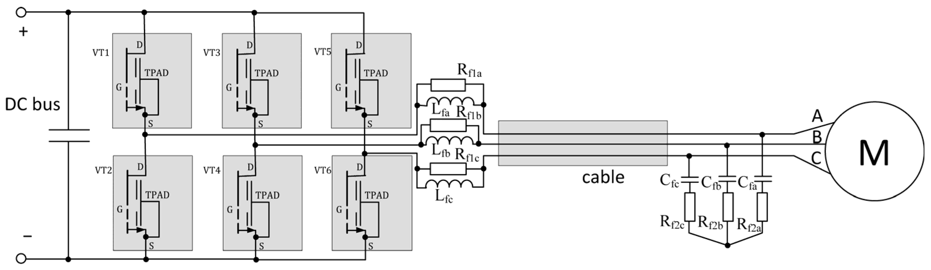
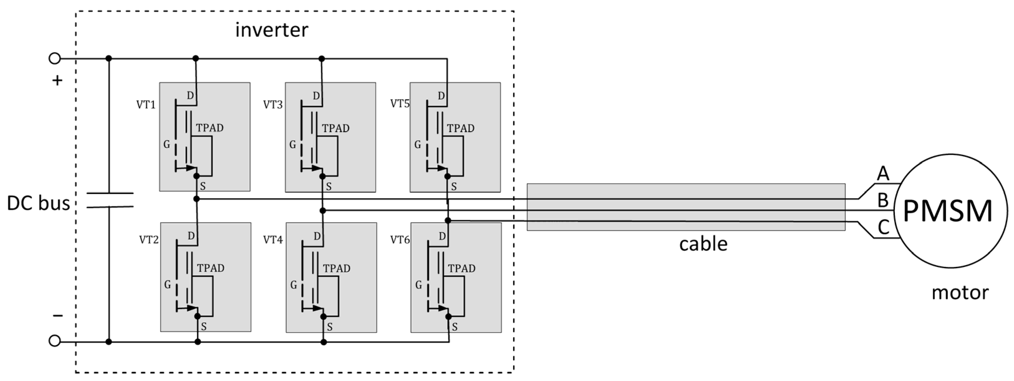
The schematics of a GaN transistor-based inverter connected to the three-phase motor through the cable can be seen in
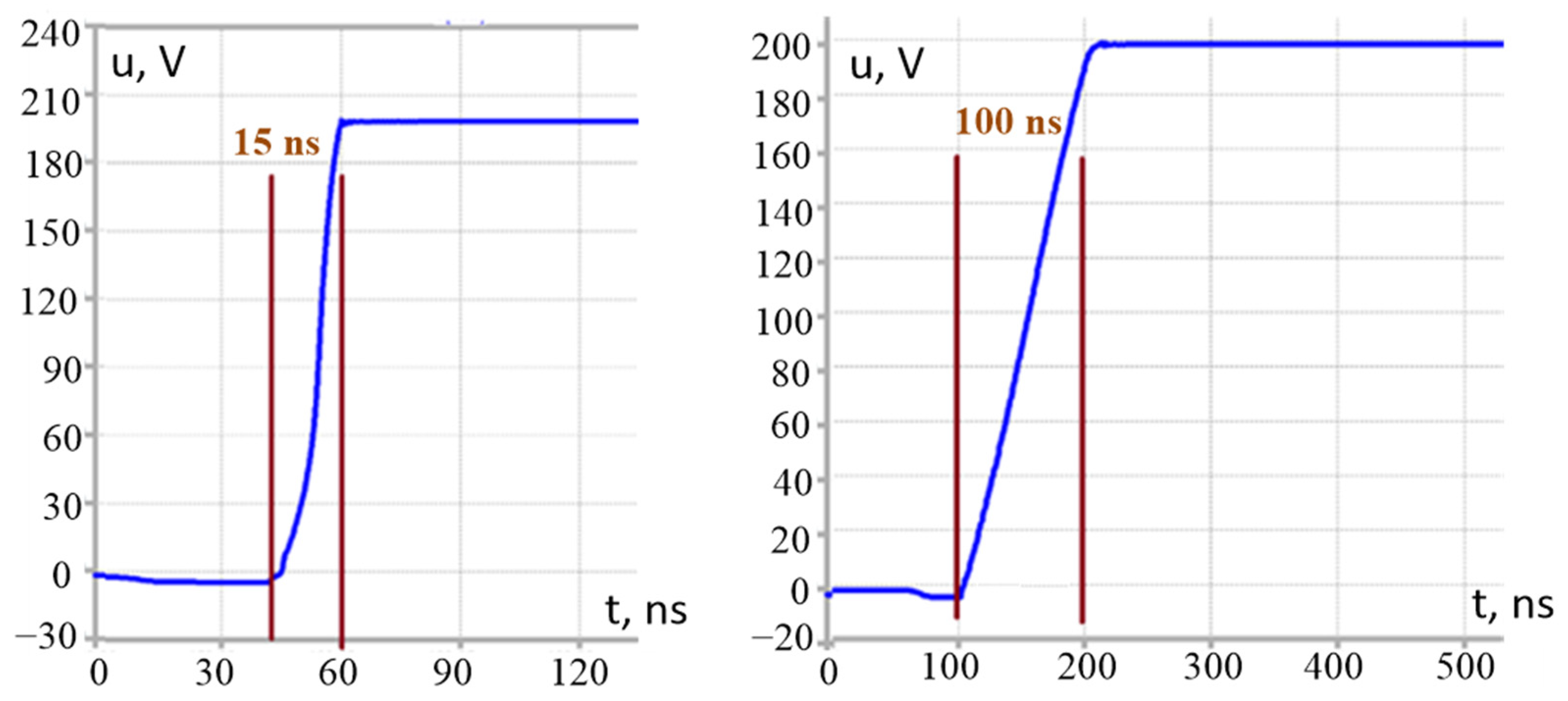
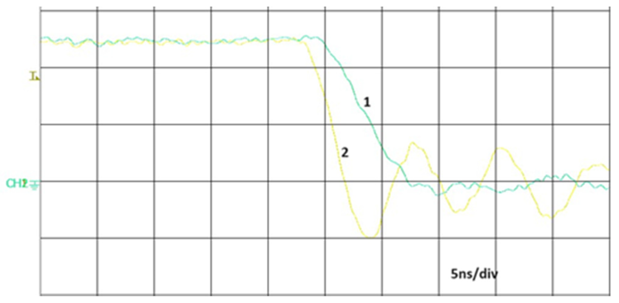
Figure 1. Fast turning on and off (high dv/dt) of GaN transistor switching action can lead to undesired oscillations and overvoltage in the cable connecting the motor and the inverter, and in the motor itself [
3,
4]. This can be explained with a parasitic capacitance and inductance of the cable and motor windings. The current in the bearing is also caused by the high dv/dt and this reduces the bearing lifespan [
5]. Magnetic bearings, shielding or insulated bearings can be used to prevent bearing damage, but that complicates the design of the motor.
Overvoltage is mainly caused by the impedance mismatch between the cable and the motor. This is often called a reflected wave phenomenon [
6], and can be characterized by the reflection coefficient:
where
ZM is impedance of the motor;
The cable characteristic impedance considering lossless transmission can be calculated as follows:
where
L0—inductance per-unit-length;
To prevent this overvoltage, this fast voltage rise time should be limited by slowing the switching action of the transistors, thus increasing switching losses, or an additional dv/dt reduction technique is required [
7], which usually adds some additional losses as well. Applications of sinusoidal filters have been analyzed in the scientific papers [
8,
9] and others. These filters have the potential to increase the system efficiency because the motor is fed with filtered, almost sinusoidal voltages, which increases the efficiency of the motor itself [
10], but the filter increases the size of the system, adds losses, and limits the torque response.
A filter placed between the drive and the motor that reduces just the dv/dt at the motor terminals is another option, which is used quite often. In [
11], the dv/dt filter and sine wave filter options were compared, and it was concluded that the dv/dt filter has a higher efficiency and smaller size. Usually, dv/dt filters have passive damping to prevent resonant oscillations. Although different solutions are proposed in the literature, with active control-based damping such as that presented in [
12,
13,
14], they are not that easy to implement and therefore classical damped filter is most often used in the industry.
In the literature, different methods have been proposed for a passive filter with passive damping design [
15,
16,
17,
18]. In [
15,
16], it was proposed to use simplified equations for filter component selection without accurate estimation of overvoltage in case of a long cable. Ref. [
17] provides the selection of RLC filter components based on simulations. In [
18], approximate value of motor impedance was used to design the filter. In [
19], the voltage reflection theory was used for optimal filer value selection. The cable itself can also be used as a part of the filter; such approach has been demonstrated in [
20,
21]. Different models of the high-frequency impedance of the cable and the motor have been presented in the literature, for example, in [
22,
23], models for motors are available. In most cases, these impedances have been used for electromagnetic emission estimation like in [
24]. At the same time, high-frequency impedance of the motor and cable can be used not only to estimate overvoltage, but also to investigate the filter influence on the overvoltage process. Such an approach will be used in this article.
In this article, different models from the literature are combined to get acceptable accuracy and to avoid very complex models. High-frequency model parameters will be estimated based on impedance measurements. The paper describes GaN transistor-based inverter prototype and suggests how to simulate the switching process of such an inverter. Next, it provides a concise, practical comparison of common filtering approaches to show that passive filtering is a competitive solution. Subsequently, it analyzes the high-frequency impedances of the cable and the motor to obtain information on overvoltage at the end of the cable. Improved solutions are proposed for distributing filter components across both ends of the cable (inverter-side and motor-side), aiming to enhance the damping performance, reduce overvoltage and oscillations, and improve overall system efficiency. To address the challenges of compactness and integration in high-frequency GaN transistor-based drive systems, this paper proposes the design of planar inductors for filter applications. Practical experimental results will be shown to verify the effectiveness of the proposed solution.
2. The Model and the Experimental Prototype of GaN Transistor-Based Three-Phase Motor Inverter
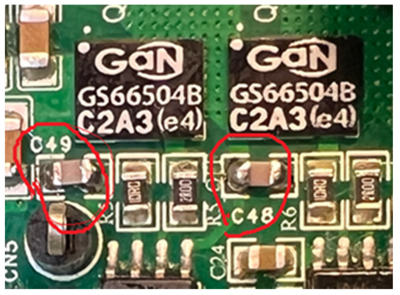
By replacing traditionally used Si transistors with GaN transistors, the efficiency of the inverter can be improved, mainly due to lower switching losses. One of the main differences from Si transistors in terms of gate control is that the gate threshold voltage VGS(th), the gate plateau and the maximum gate voltage VGS(max) are lower. To turn off the GaN semiconductor, the gate voltage should be maintained below the minimum gate threshold voltage, which is around 1 V. This can be a challenge in the applications where the GaN transistor drain is exposed to a high dv/dt, as undesired turning on of the transistor can occur. Gate drivers must have high common-mode transient immunity. The integrated circuit of the driver should be placed near the transistor gate to limit stray inductances and capacitances. High dv/dt causes high common-mode currents; this is the reason why it is important to minimize coupling capacitances of an isolated power supply and use a gate driver with high common-mode transient immunity.
The electrical circuit of the three-phase inverter can be seen in
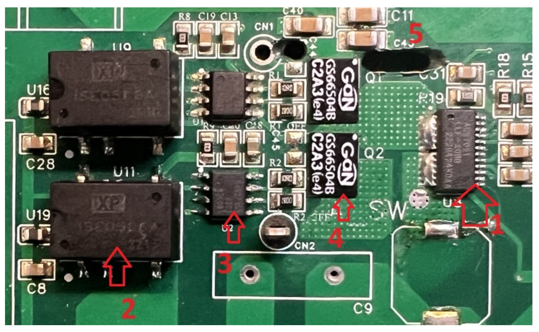
Figure 1. It consists of six transistors that are connected to each motor phase and powered by a DC voltage source or rectified AC voltage. To control the motor, a digital controller is used, which measures the currents and voltages and controls the speed and the torque. Considering the previously mentioned experimental inverter design, isolated driver circuits have been selected. Part of the inverter’s printed circuit board (PCB), which includes one half-bridge of the transistors and the driver, can be seen in
Figure 2. To isolate the gate-driving voltages, low-power switched-mode power supplies (2) with high isolation voltage and low capacitance between primary and secondary side have been selected. The driver circuit (3) and half-bridge of the GS-065-004-1-L GaN transistors (Infineon, Neubiberg, Germany) (4) can be seen in
Figure 2. For current measurement, hall effect-based current sensor (1) is also placed on the board.
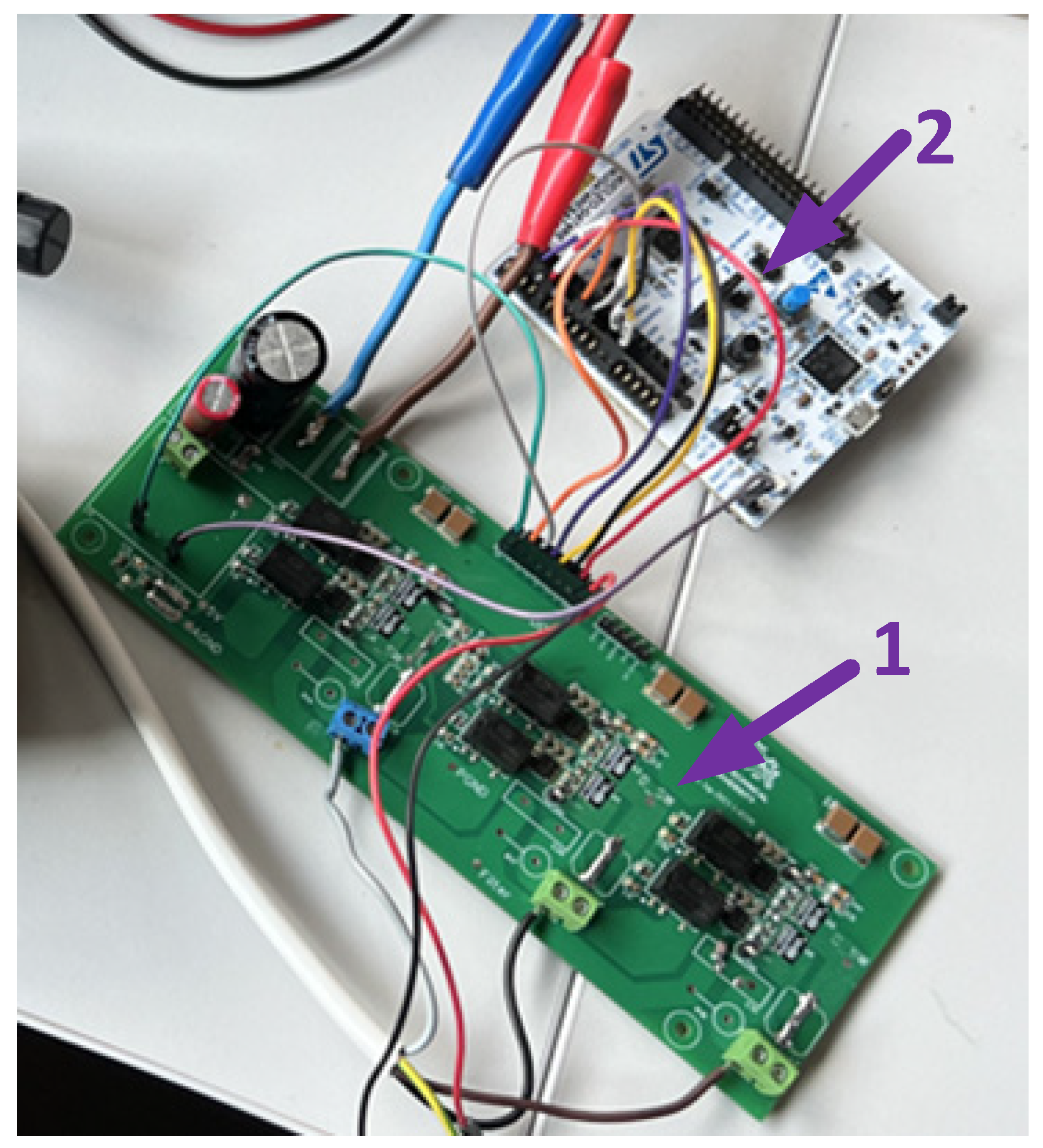
The developed PCB of the three-phase motor inverter can be seen in
Figure 3. A STM32G411 microcontroller (STMicroelectronics, Geneva, Switzerland) has been used to control the inverter. This microcontroller offers features like filter math accelerator (FMAC), high-resolution timer (HRTIM), with the ADC and processor working at a frequency up to 170 MHz and are available for relatively low cost. This microcontroller is suitable for controlling power electronics converters and electrical drivers due to advanced driver capability.
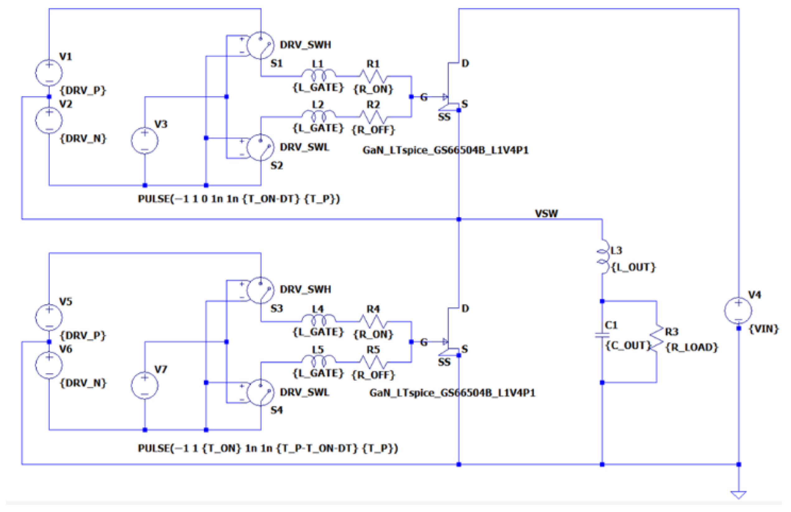
To investigate the voltage reflection and to test different filter designs, a simulation model has been created. The simulation model consists of one leg of the inverter that is very similar to synchronous buck converter. The simulation was created in LTSpice XVII simulation software. This simulation model can be seen in
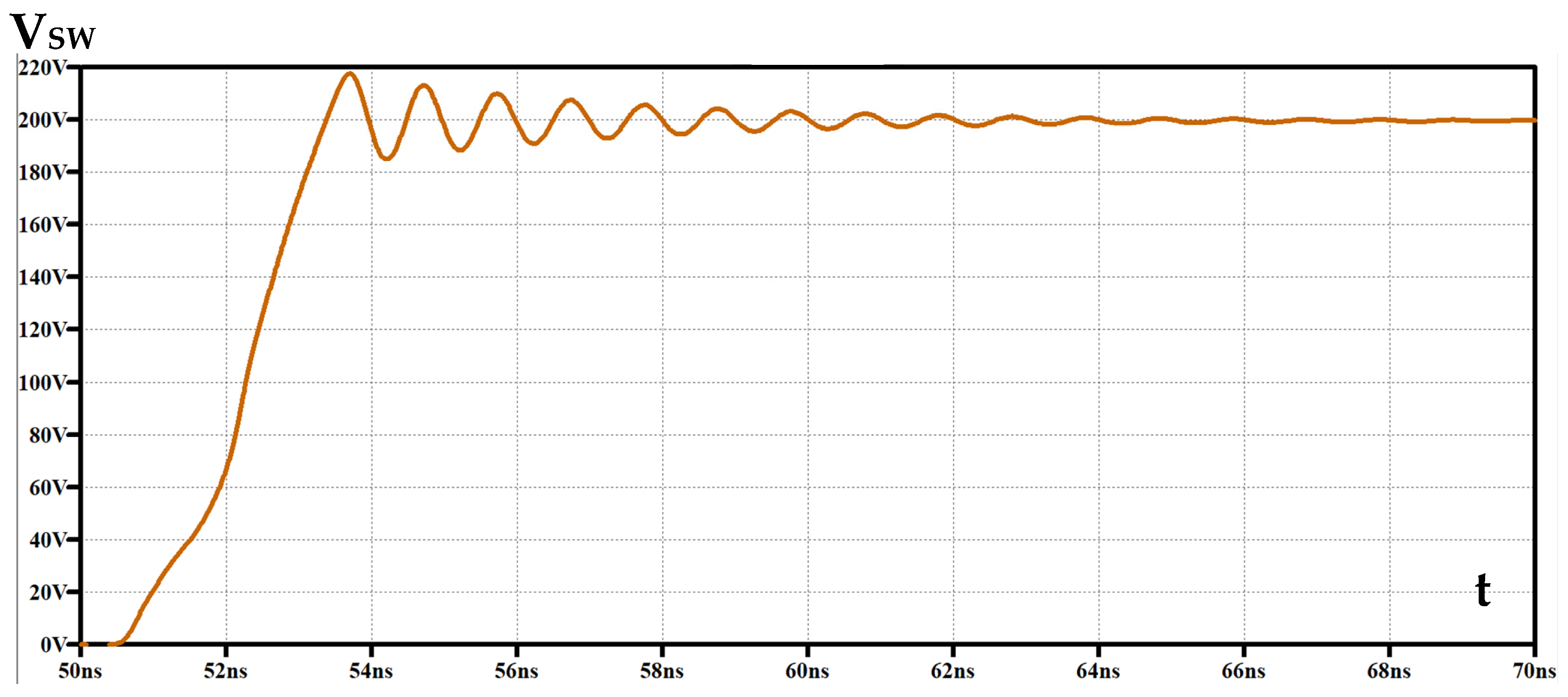
Figure 4. To verify the accuracy of the Spice model of the transistors, simulation-based results were compared with experimental ones. The voltage can be seen in
Figure 5 between the drain and the source of one of the transistors, which is the switching node voltage V
SW. The curve was obtained from the LTSpice simulation model shown in
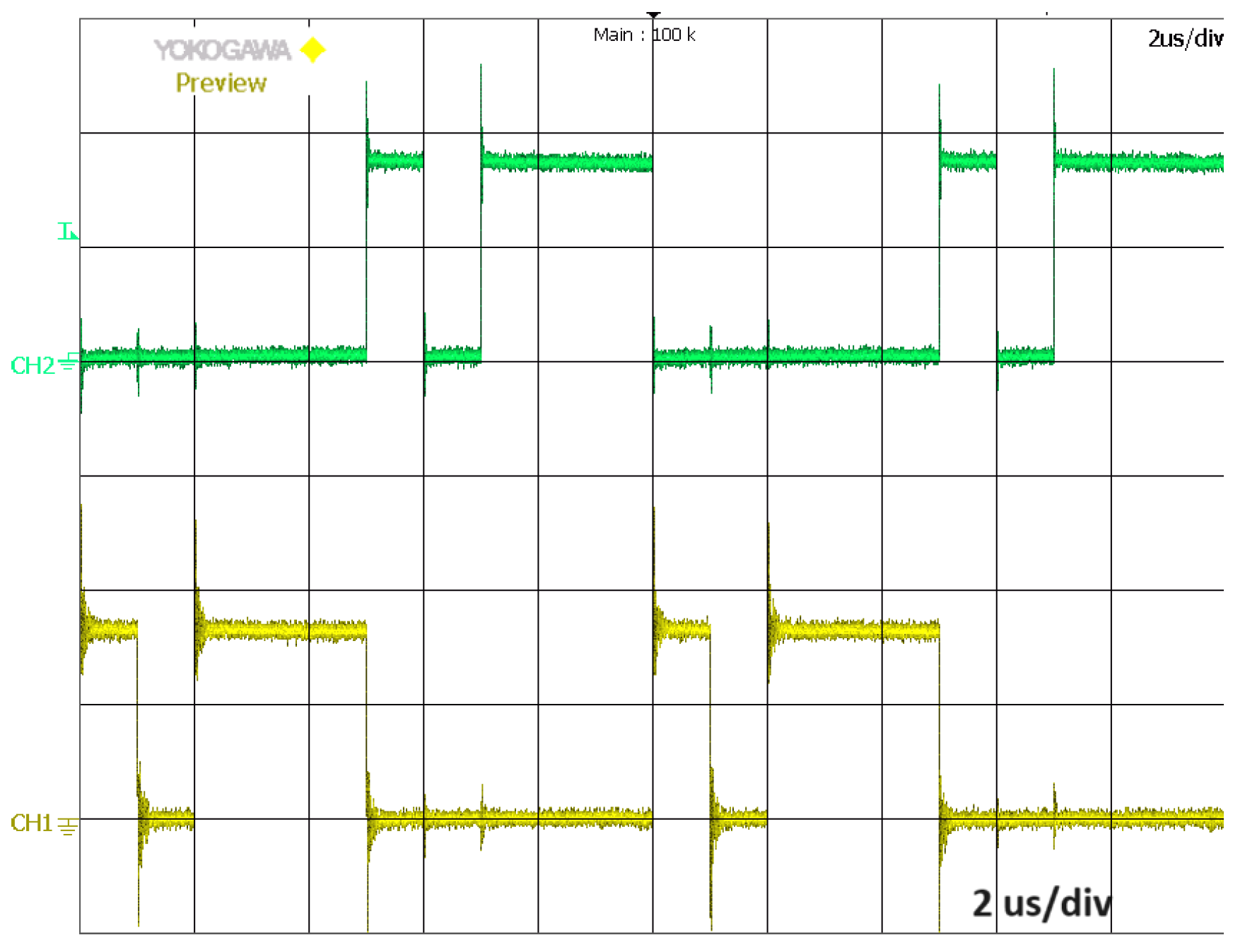
Figure 4. Additional inductance was placed on the DC bus to adjust the waveform to be like the experimental one. In the simulation, the duty cycle is 0.5 and the driving pulse was supplied to the driver at the 50th nanosecond. The oscillations are caused by parasitic inductance of the PCB traces, capacitor parasitic inductance, and the package of the transistors. This inductance can be measured, calculated or adjusted to fit the experimental waveform as in this case. If a proper inductance value is added to the simulation model, then it describes the transient process with high accuracy, and this simulation model can be used to analyze the overvoltage and different filter solutions. Only an accurate enough high-frequency model of the cable and the motor itself are needed.
3. High-Frequency Model of the Cable and the Motor
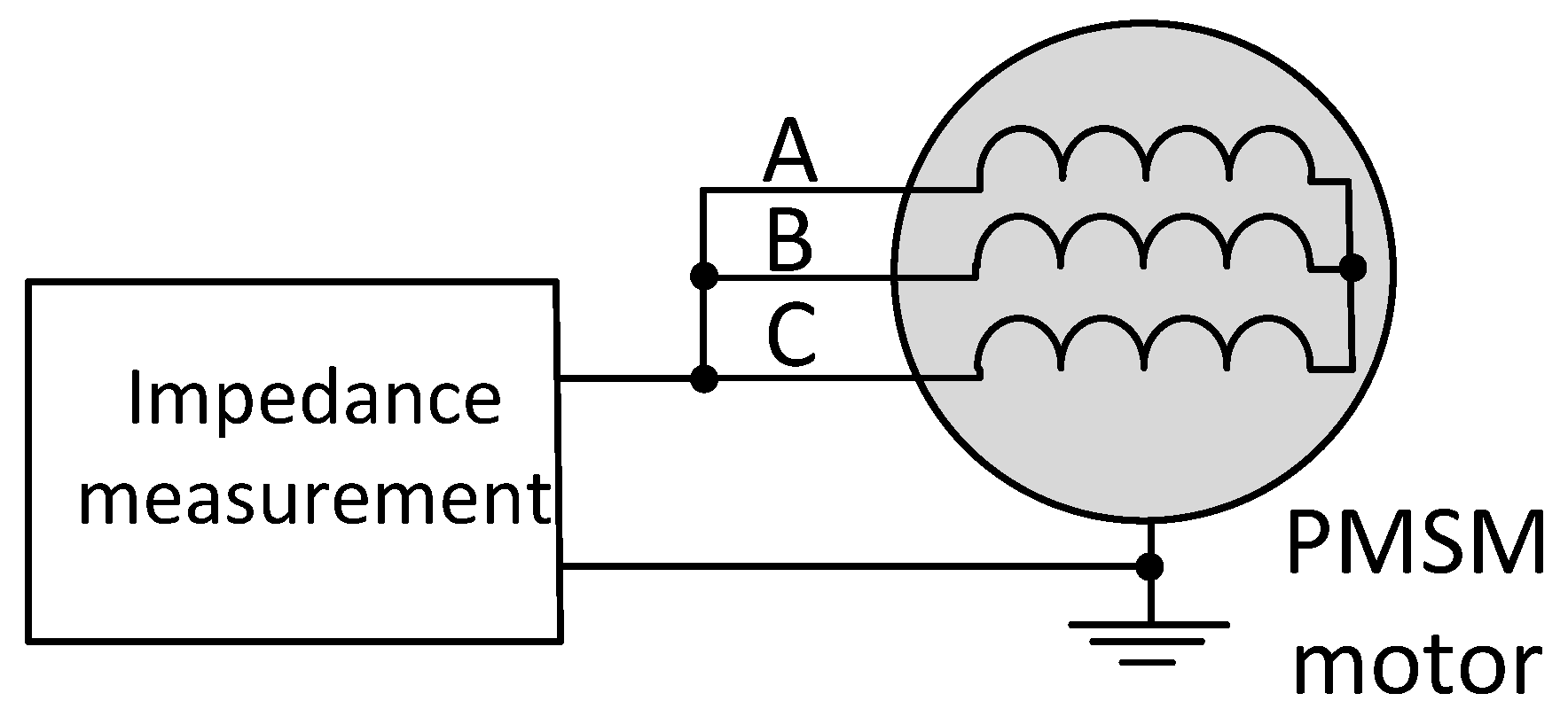
To understand the process of reflection and to develop solutions to mitigate these effects, it is important to obtain the high-frequency models of the electrical motor and the power cable connecting the inverter and the motor. The parameters of the equivalent circuit can be determined by measuring the differential-mode (DM) and common-mode (CM) impedance of the cable and the motor in the frequency domain [
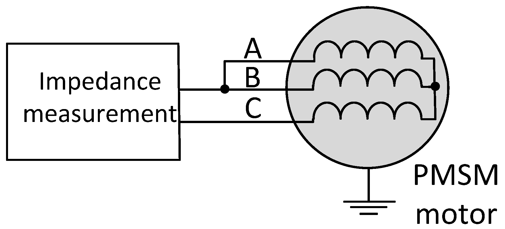
25]. The connections to measure such impedances can be seen in
Figure 6 and
Figure 7. In a similar way, the cable was connected for the measurements of the impedance.
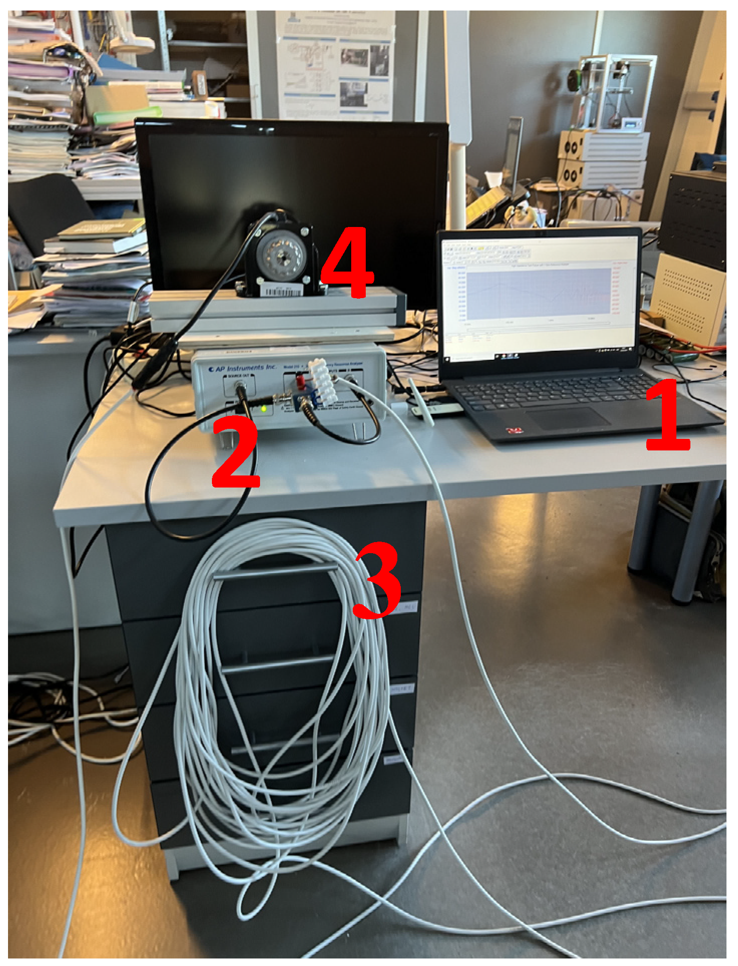
The experimental measurement setup can be seen in
Figure 8. To measure the impedance, an AP310 (Ridley Engineering, Camarillo, CA, USA) frequency response analyzer (2) was used, and the data were transferred and stored on the laptop (1). For the experiments, a 1 kW 3000 rpm MXL-10A0830FA222 (Trio Motion Technology, Tewkesbury, UK) PMSM motor (4) was used. A 33 m long cable consisting of 4 wires with a 0.75 mm
2 cross-sectional area (3) was used for this research.
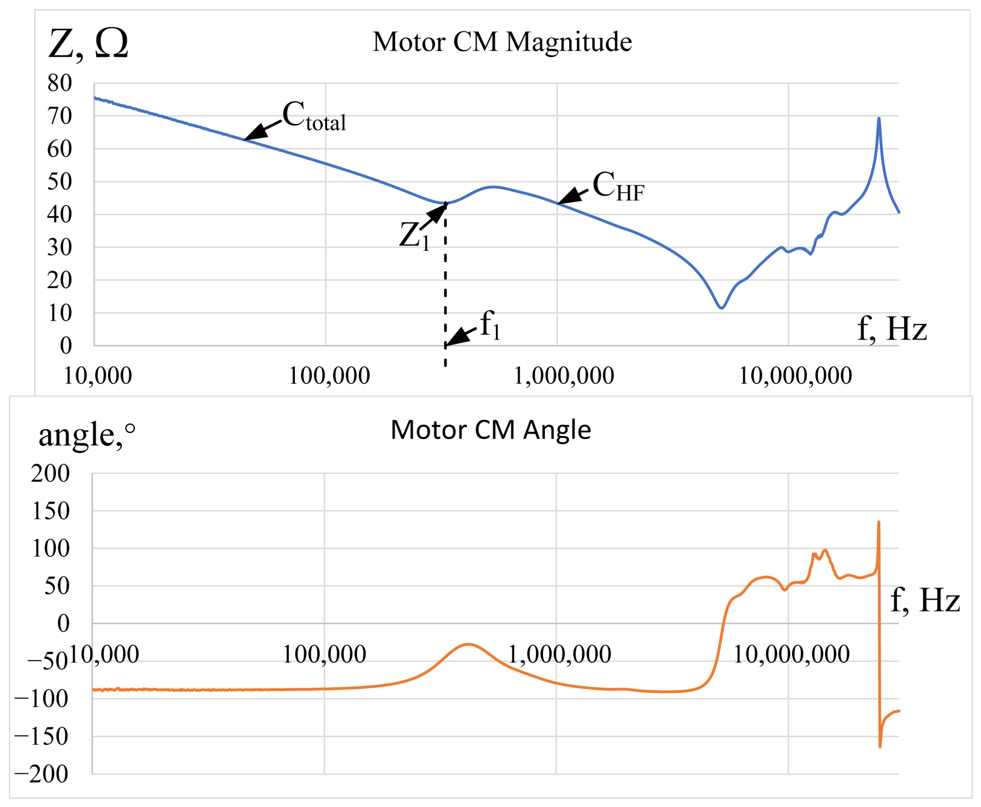
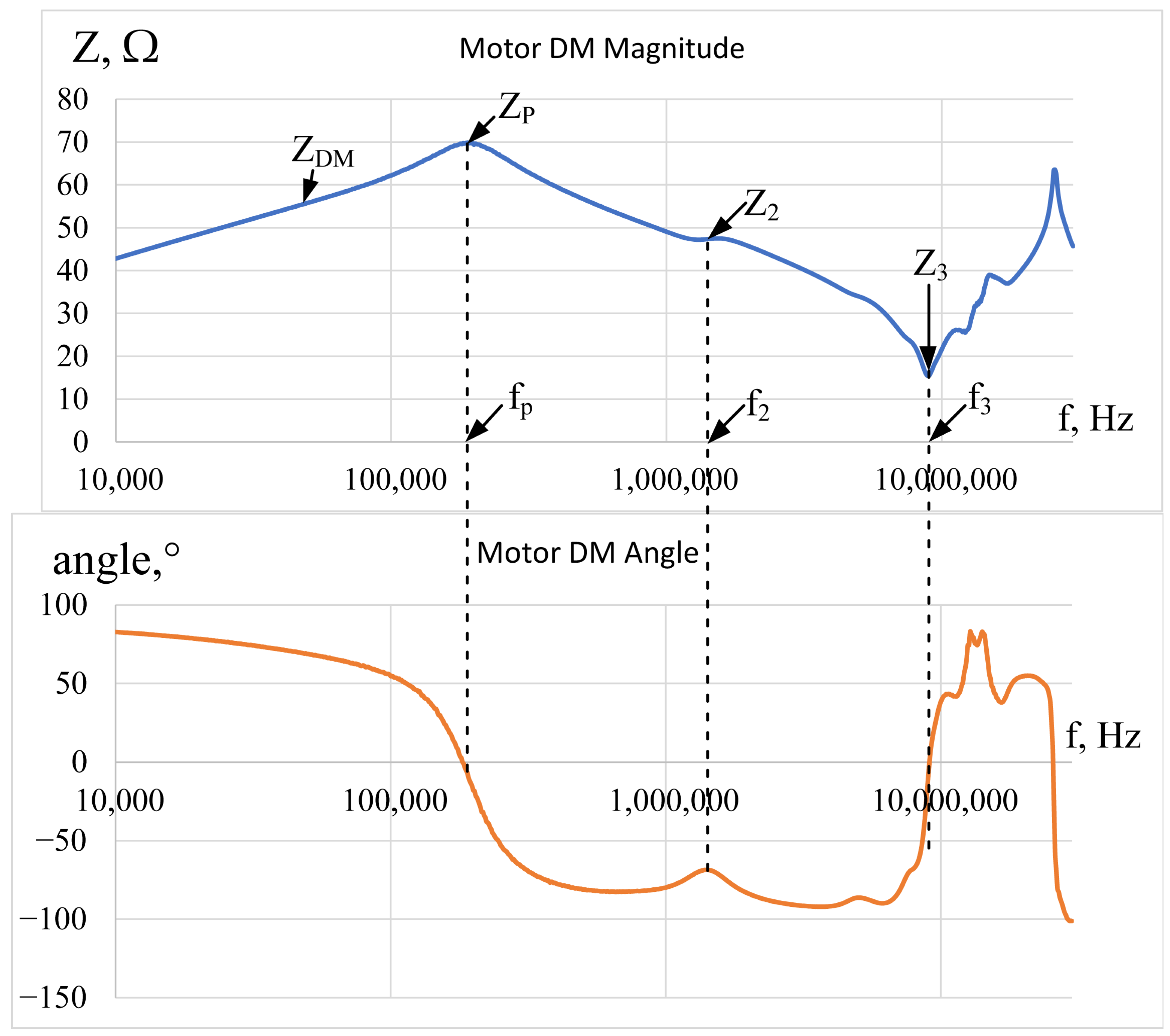
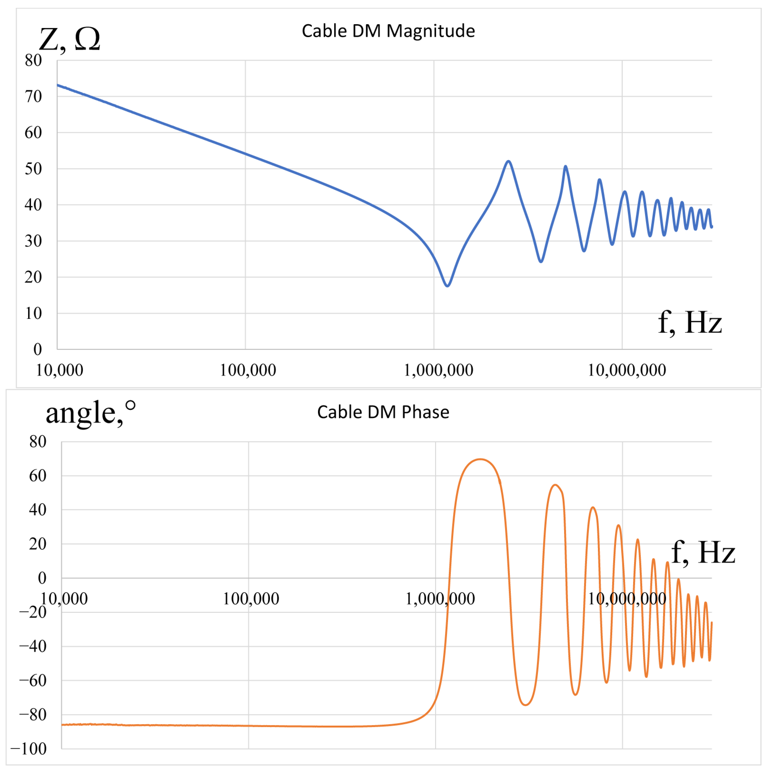
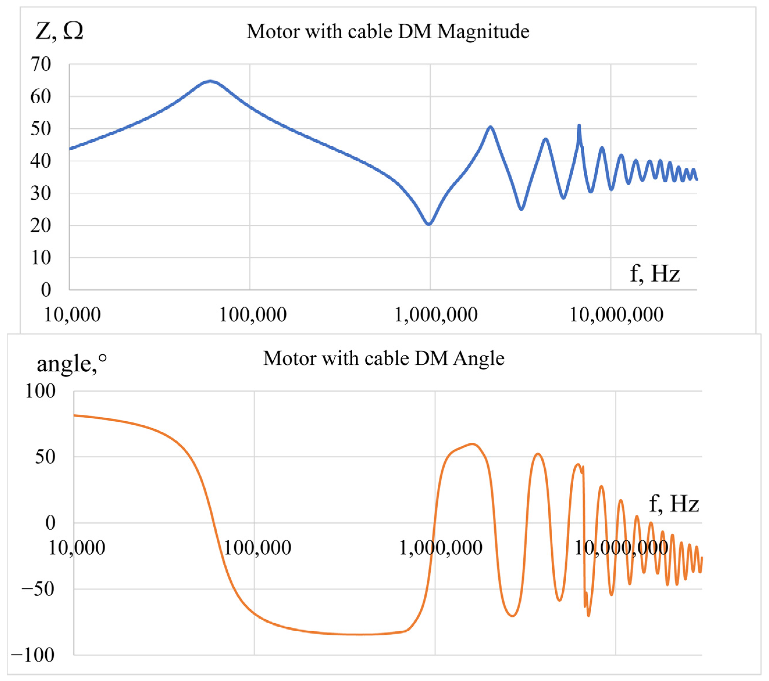
The measurement results can be seen in
Figure 9,
Figure 10,
Figure 11 and
Figure 12. From these measurement results, it is possible to obtain the values of the equivalent circuit representing the motor and the cable for high frequencies. In the literature, several equivalent circuits have been proposed that describe motor or cable impedance with good accuracy. In Ref. [
26], a circuit has been proposed that models the AC motor, including the high-frequency model and the dynamic dq model; other equivalent circuits have been proposed in [
24] for electromagnetic emission investigation. In Ref. [
27], a lumped-parameter cable model has been proposed. The review of different motor models can be found in [
3], where it is stated that in the case of a PMSM motor, the position of the rotor can influence impedance graph, but in this particular case such a impact has not been observed by practical measurements. A more complex model can be found in [
28]. In this case, a similar model was used as in [
29], where a universal high-frequency model of induction motor was proposed. The values of model elements can be obtained from the measured impedance curves.
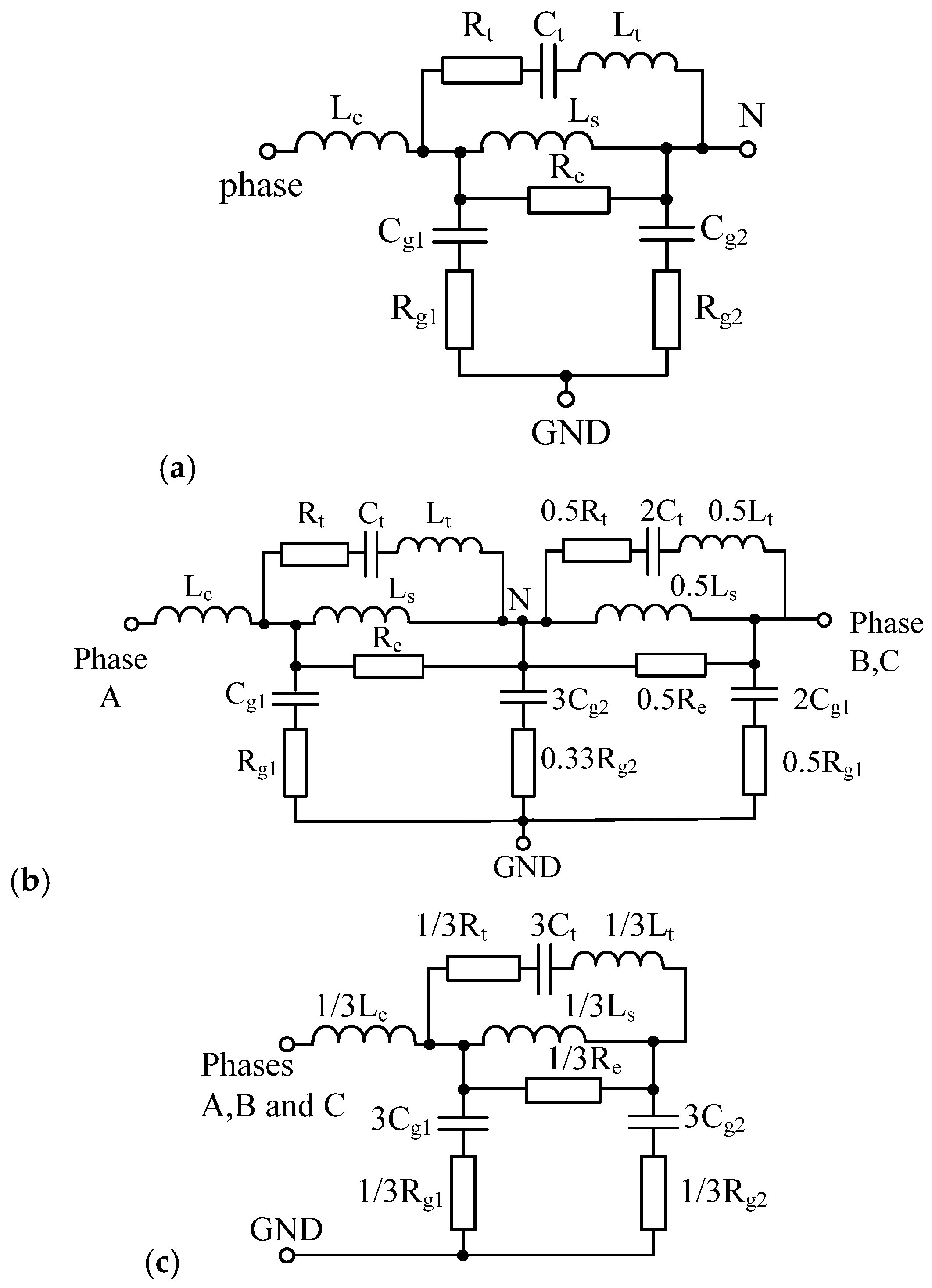
In
Figure 13, high-frequency differential mode and common models of the motor can be seen. The values of model elements can be obtained from the measured impedance curves [
29]. The measured DM and CM impedance magnitudes and phases and the most important points for the model characterization are shown in
Figure 9 and
Figure 10. The total winding-to-ground capacitance
Ctotal and the high-frequency winding-to-ground capacitance
CHF can be extracted from the slopes of common-mode impedance shown in
Figure 9.
Ctotal characterizes the low-frequency range of curve shown in
Figure 9, but C
HF is the straight section of the impedance curve at a high frequency. From that graph, for motor impedance measurements, values of
Ctotal and
CHF can be estimated by selecting random point on these straight sections of curve where the phase is close to −90°, as shown in
Figure 9 and
Figure 10, and calculating the capacitance using the well-known equation (C = 1/2πfZ). Capacitances
Cg1 and
Cg2 used in the motor are as follows [
30]:
The winding-to-ground equivalent resistances,
Rg1 and
Rg2 are calculated from the impedance
Z1 resonant point shown in
Figure 9 and the impedance
Z3 resonant point in
Figure 10. These resonance points can be recognized at the place where the straight curve changes direction and the phase is close to 0°. At these resonance points, inductive impedance compensates for capacitive impedance and impedance is equal to resistance. Corresponding resistances in the motor equivalent circuit can be calculated as follows:
The differential-mode inductance
LDM can be calculated from measured differential impedance shown in
Figure 10 by selecting some random point on the low-frequency slope where the phase is close to 90° and calculating using the well-known equation (L = Z/2πf). In this case, this inductance is equal to 2 mH. Common-mode inductance
LCM can be calculated using the impedance Z
1 at the resonant point, at which capacitive impedance is equal to inductive impedance and thus it can be calculated as follows:
Stator leakage inductance
Ls can be obtained from previously obtained inductances as follows [
30]:
The high-frequency loss resistance
Re, similarly to
Rg1 and
Rg2, can be determined from the resonant point impedance
ZP in
Figure 10 as follows:
The capacitance
Ct can be determined as follows [
26]:
The inductance
Lt and resistance
Rt for the series resonance are calculated from the impedance
Z2 at the resonant point as follows [
23]:
where
ΘZ2 is the phase angle at frequency
f2 from measured differential mode impedance shown in
Figure 10.
Inductance
Lc can be calculated from the resonant point
Z3 at which capacitive impedance is equal to inductive impedance as follows from [
29]:
The values of the elements of the high-frequency model of the motor calculated by Equations (3)–(13) can be seen in
Table 1.
From the cable differential-mode impedance shown in
Figure 11 capacitance, inductance and resonant frequency can be determined in a similar way, as in the case of the motor model.
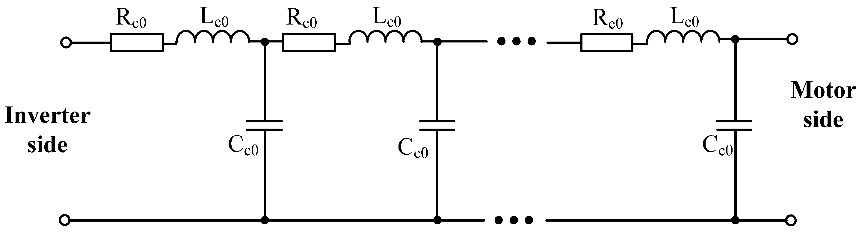
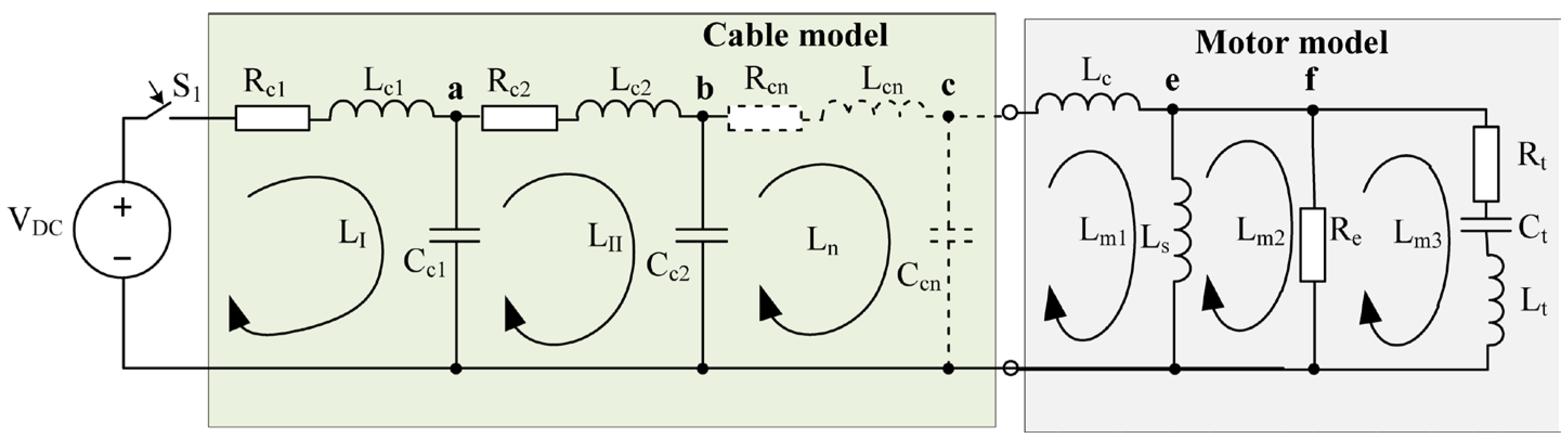
Simple models consisting of RLC branches are mostly used for cable modelling. The electrical circuit of such a model can be seen in
Figure 14. The impedance of the cable can be calculated from the geometrical parameters of the cable; a simplified equation has been presented in [
31]:
where
z—thickness of the insulation of the cable strands;
d—diameter of the copper of the cable strand.
From the impedance curve, the determined capacitance is
C0 = 110 pF/m, and the inductance is equal to
L0 = 0.53 µH/m, while resistance
R0 = 20 mΩ/m. The corresponding cable impedance, calculated by (2) and (14), is approximately equal to 67 Ω. The propagation delay in the long cable can be calculated as follows:
where
l is the length of the cable. In this case, by using (15), it can be determined that propagation delay is equal to 250 ns.
Also, there is a possibility to use more complex cable models such as those presented in [
25,
26,
32]. One such more complex model, based on
Figure 12 and the approach given in [
29], has been created, and the obtained simulation results gave just less than a 15 percent difference compared to the simplified model, meaning that the use of simplification is acceptable for the overvoltage filter design.
The accuracy of the model also depends on the number of branches employed, although this factor has only a minor influence. To evaluate the impact of the filter components on overvoltage reduction, the equivalent circuit shown in
Figure 15 was used. Kirchhoff’s voltage law was applied to derive the governing equations, which were subsequently solved using numerical methods. Kirchhoff’s voltage laws have been applied to obtain equations that can be solved by using numerical methods. In this case, Wolfram Mathematica software was utilized. To reduce the complexity and time required for the calculation, the cable model was limited to four branches.
4. Overvoltage at the Motor Terminals
The long cable combined with high dv/dt of GaN transistors causes reflections which are leading to overvoltage. The reflection coefficients at the motor side (
Γmot) and at the inverter side (
Γinv) are often used to describe the process in the cable; the reflection coefficient at the motor side can be calculated as follows:
where
Zm is the motor impedance;
Zc is the impedance of the cable. The reflection coefficient at the inverter side can be calculated as follows:
where
Zm is the motor impedance.
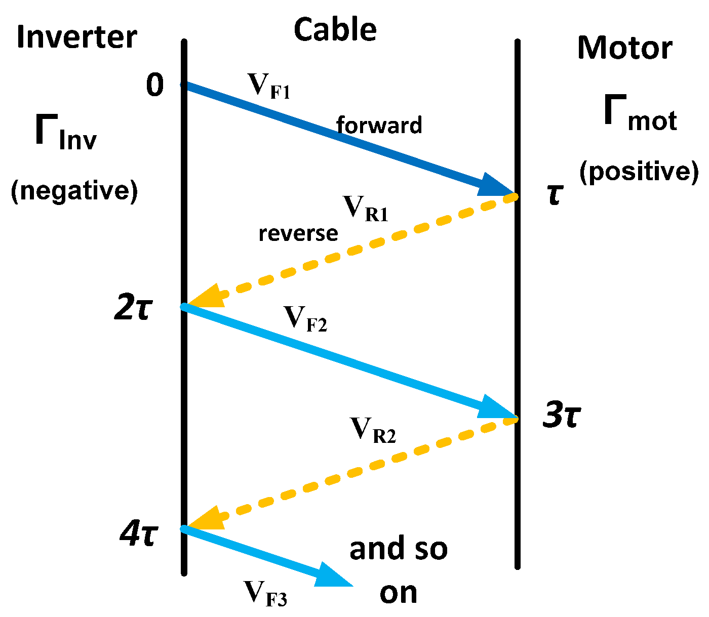
As the impedance of the motor is usually higher than the impedance of the cable, the reflection coefficient is positive and, in the worst case, it can be equal to 1. In that case, the voltage will reach two times higher voltage than the DC voltage, which can destroy the isolation of the motor. The impedance of the inverter is low and, therefore, the reflection coefficient at the inverter side is usually negative. This is the reason why the third reflected wave is negative and is going to reduce the further growth of the voltage. This reflection process can be seen in
Figure 16.
The simulation model shown in
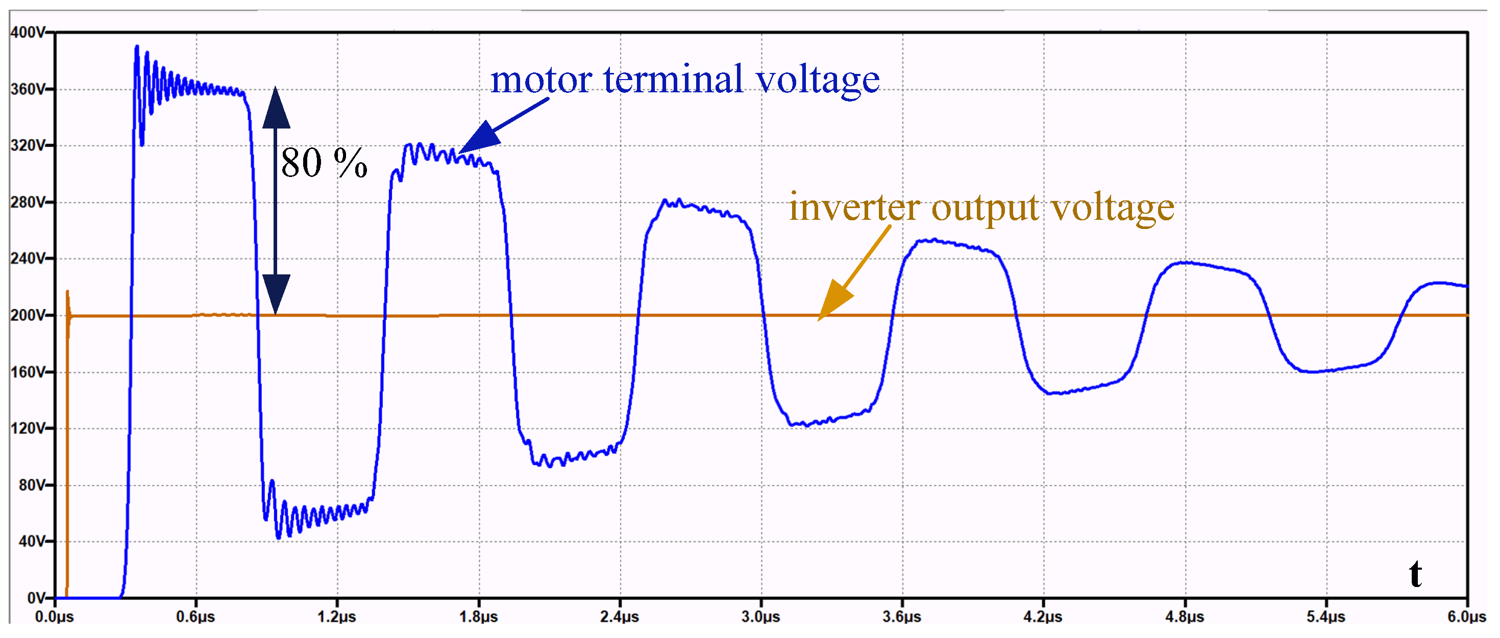
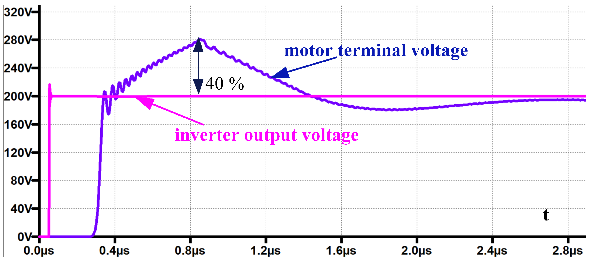
Figure 4 has been extended with the cable and motor equivalent circuits obtained previously. The cable was simulated in the LTSpice software with 33 branches connected in the series connection. As a simulation result, it is possible to obtain the voltage at the motor terminal, which can be seen in
Figure 17.
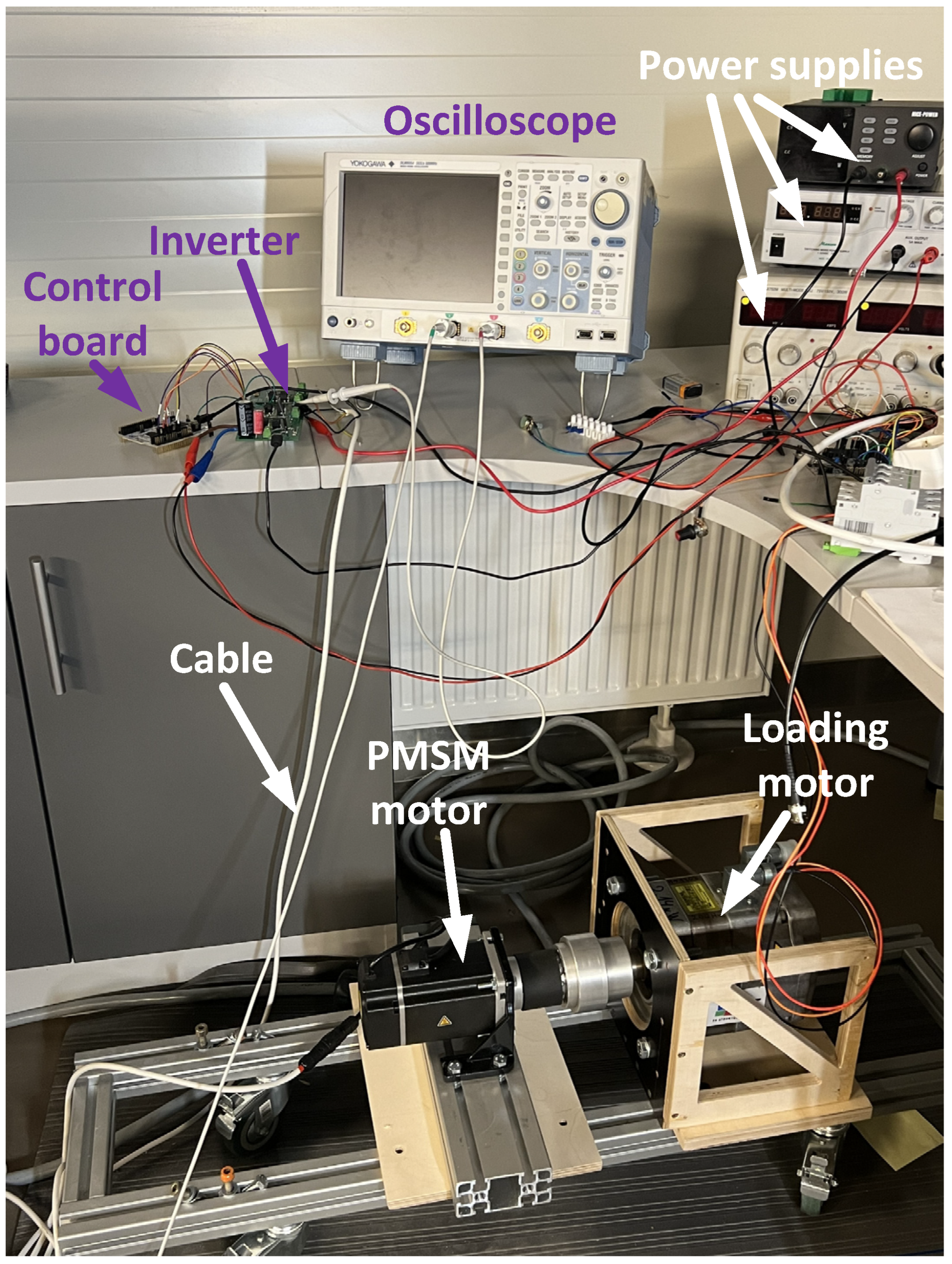
Similar results can be measured experimentally by supplying the PMSM motor through the long cable with high dv/dt signals generated by GaN transistor-based three-phase inverter. An experimental setup can be seen in
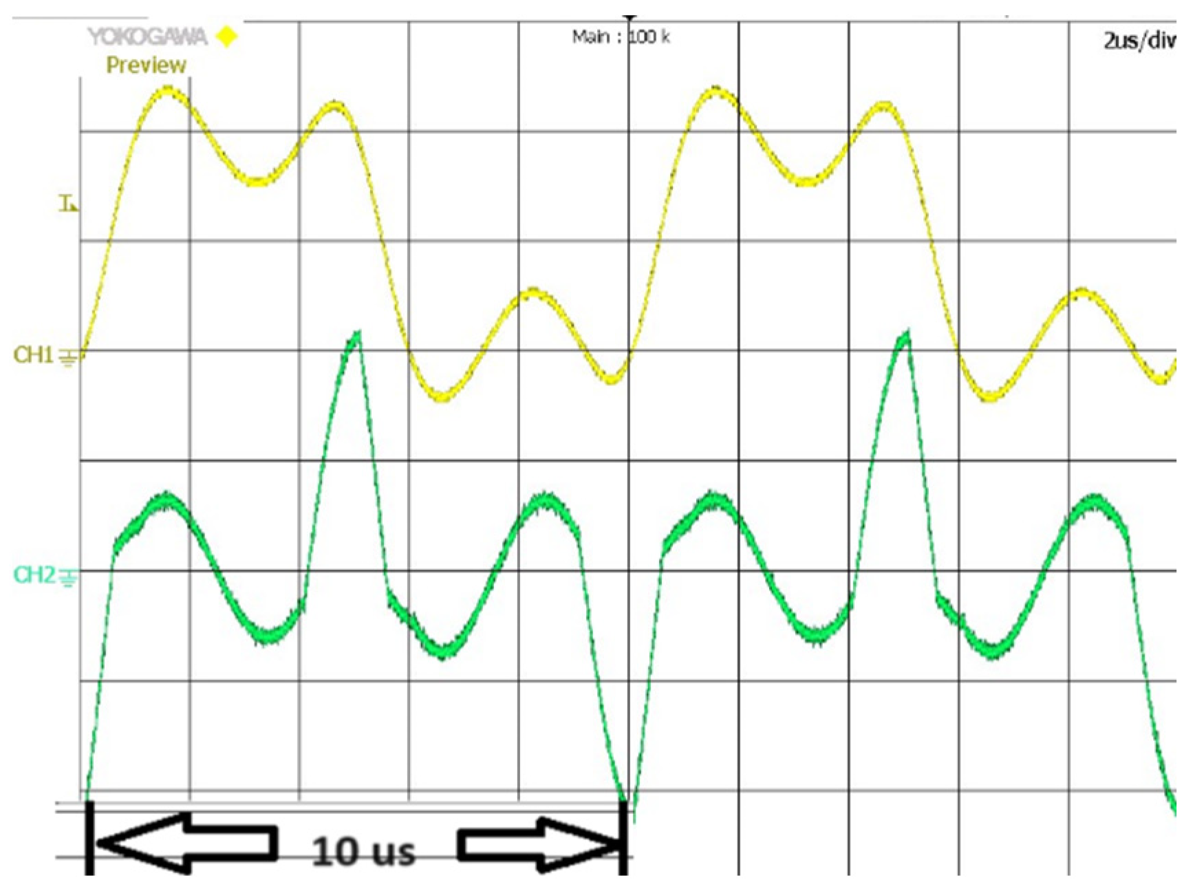
Figure 18. The signals measured by the oscilloscope can be seen in
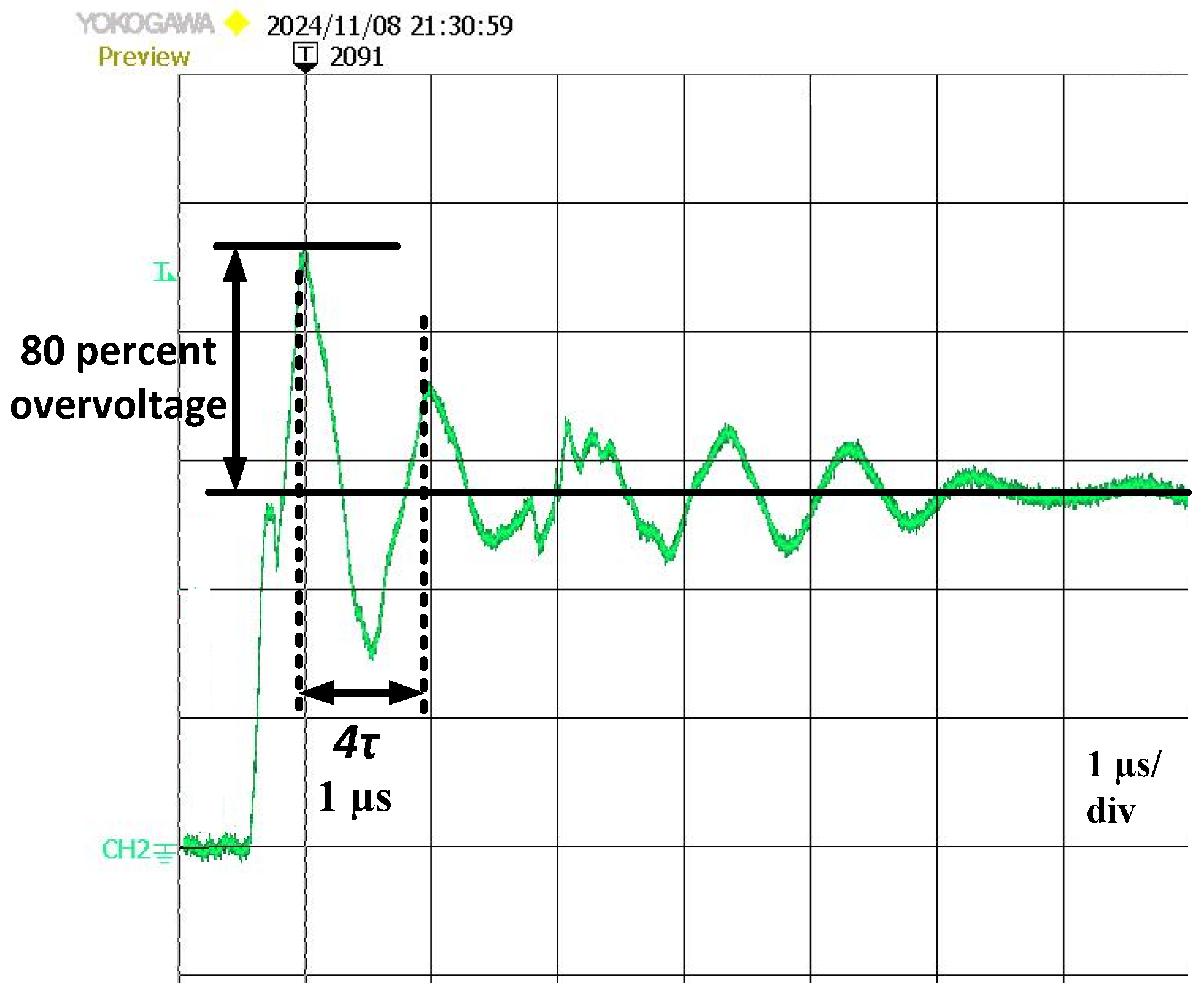
Figure 19. Around 80 percent overvoltage was observed in simulations and experiments. Experimental results confirm the previously determined propagation delay, which can be determined from the interval between two peaks which takes four reflections. Since the simplified model of the cable is used, the waveform is not fully accurate, but describes the overvoltage and the waves travelling into the cable with good enough accuracy.
For the reflection process and overvoltage analysis, different approaches can be used. The traditional theory of long lines with distributed parameters can be used for analysis, but for practical applications, these equations are too complex. A simplified expression for overvoltage calculation can be found in [
33] and in other sources:
where
v—propagation speed of the wave in the cable;
tr—rise time of the voltage of the transistor.
As can be seen from (18), overvoltage depends on several parameters: the DC bus voltage UDC which is fixed, and the propagation speed v that depends on the cable parameters and is constant as well. Mainly, two approaches can be used to reduce overvoltage—influencing the reflection coefficient or changing the rise time of the voltage.
6. Improved Filter for Overvoltage Mitigation of High Switching Frequency Inverter
As was mentioned previously, the high inductance of the inductor in the case of the GaN inverter with high switching frequency cannot be used, and full overvoltage reduction with RL filter is challenging. In
Figure 26, a case can be seen when a reduction RL filter with 25 µH inductor and 67 Ω resistor has been used for overvoltage. As can be seen, overvoltage still exceeds 40 percent.
Another option is to use the RC filter at the motor side. To calculate the values of RC filter, the methodology presented in [
19] can be used. In Ref. [
19], developing the filter at the motor side has been proposed, which creates negative reflection coefficient. The value of R
f2 is selected equal to
Z0/2 and capacitor value is calculated by the following equation:
where
l is the length of the cable,
C0 is the equivalent capacitance of the cable per metre and
Γmot is the reflection coefficient at the motor side, which can be calculated by (1) or determined from
Figure 19 to be approximately equal to 0.8.
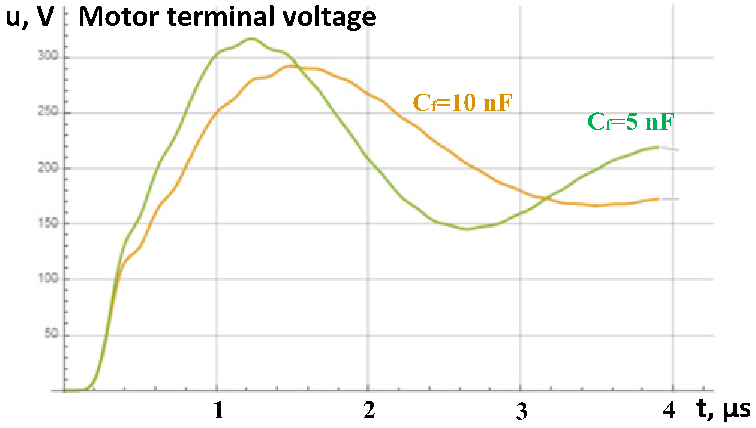
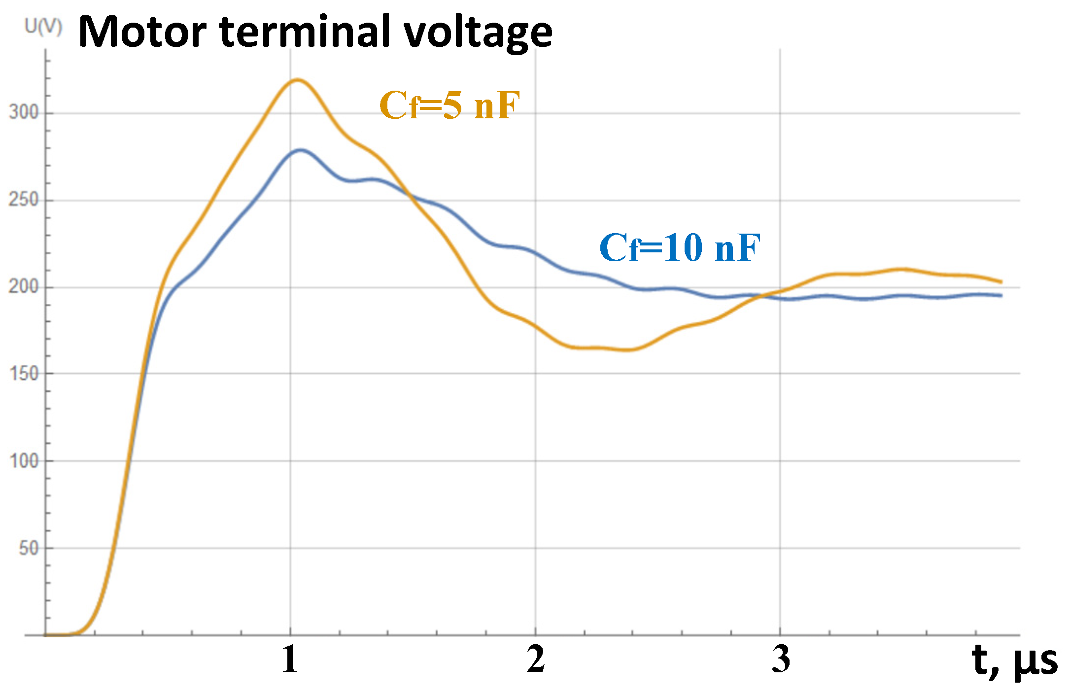
Figure 27 shows the curves for the case if R
f2 is equal to
Z0/2 at different values of filter capacitor, obtained by analytically solving the circuit shown in
Figure 15 with the added RC filter. As can be seen, the overvoltage is being reduced, but overvoltage reduction is similar to the case of the RL filter, since it is not possible to use the high capacitance for the filter to maintain the losses in the filter resistor in the decent range.
The second option is to use
Rf2 equal to
Z0 and select a capacitor value to provide significant impedance at the switching frequency and reduced impedance above this frequency. The results can be seen in
Figure 28; the overvoltage reduction is slightly better than in the case when
Rf2 is equal to
Z0/2.
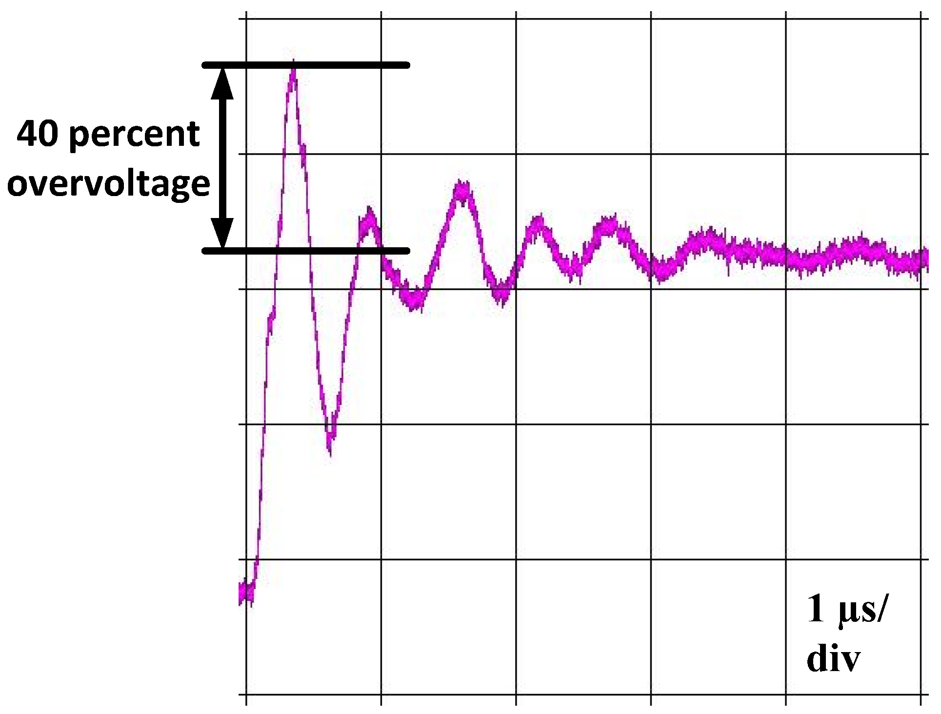
Figure 29 shows experimental results with an added RC filter to the end of the cable. As can be seen, the overvoltage is reduced, but still, it is quite high—in the range of 40 percent. The result is quite like the simulation and the analytically obtained results. To reduce overvoltage further, the filter should be improved.
To reduce overvoltage more, the RL filter can be combined with an RC filter at the motor side. The circuit can be seen in
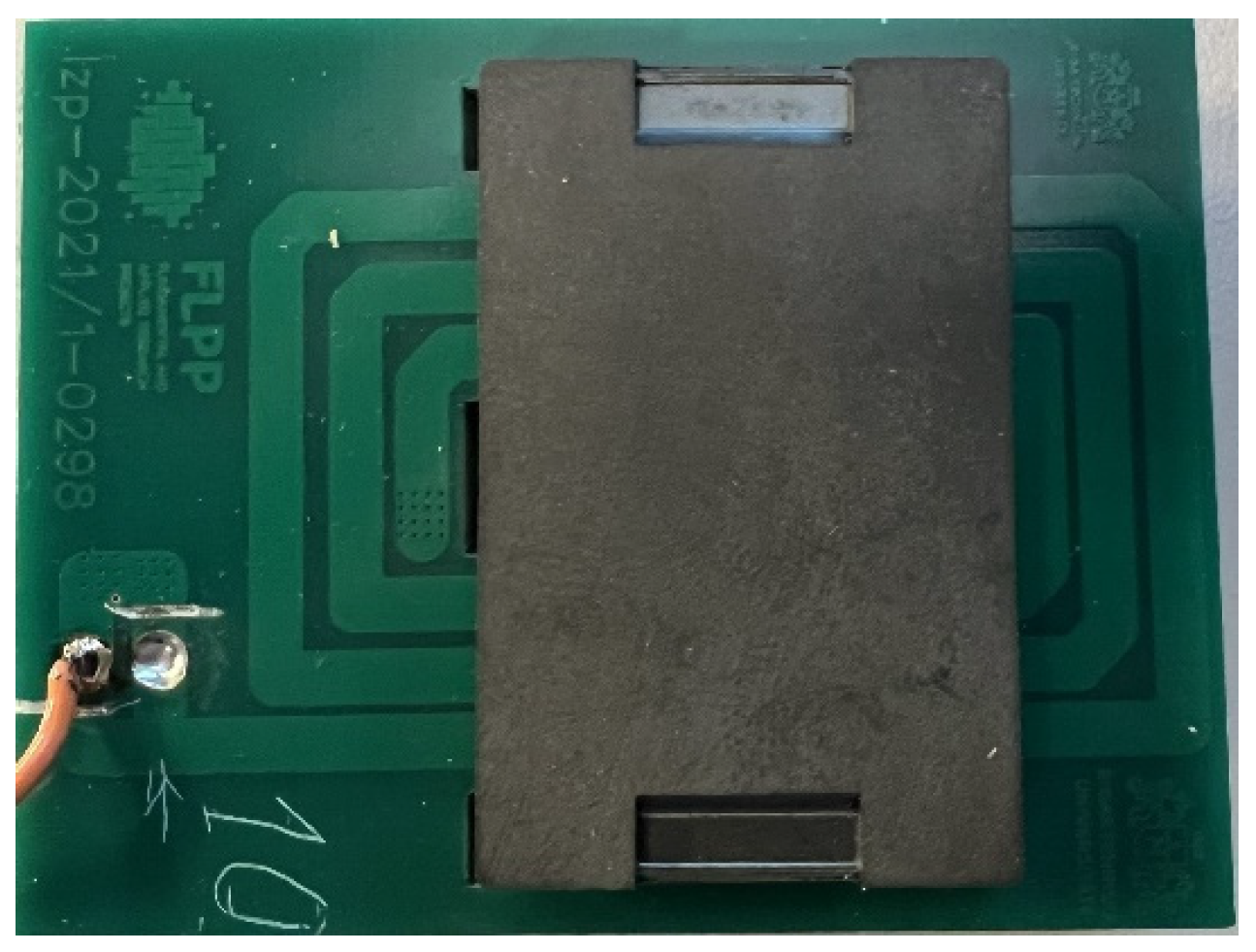
Figure 30. Since the desired switching frequency of the inverter has been selected to be equal to 50 kHz, the inductor is selected equal to 25 µH. Higher inductance will increase the impedance, and a significant part of the current is going to flow through the resistor and is going to increase the losses. To reduce the size of the RL filter inductor in this case, planar inductors have been developed. The manufacturing process of such inductors can be automated, and the size is being reduced due to the planar core. In
Figure 31, a developed planar inductor can be seen; in the design of inductor ELP 43/10/28 N87, material core has been used. The inductor consists of three PCB-based windings on the top side and three windings on the bottom side of the PCB. Six PCBs are soldered together to create a series connection of 36 windings.
In
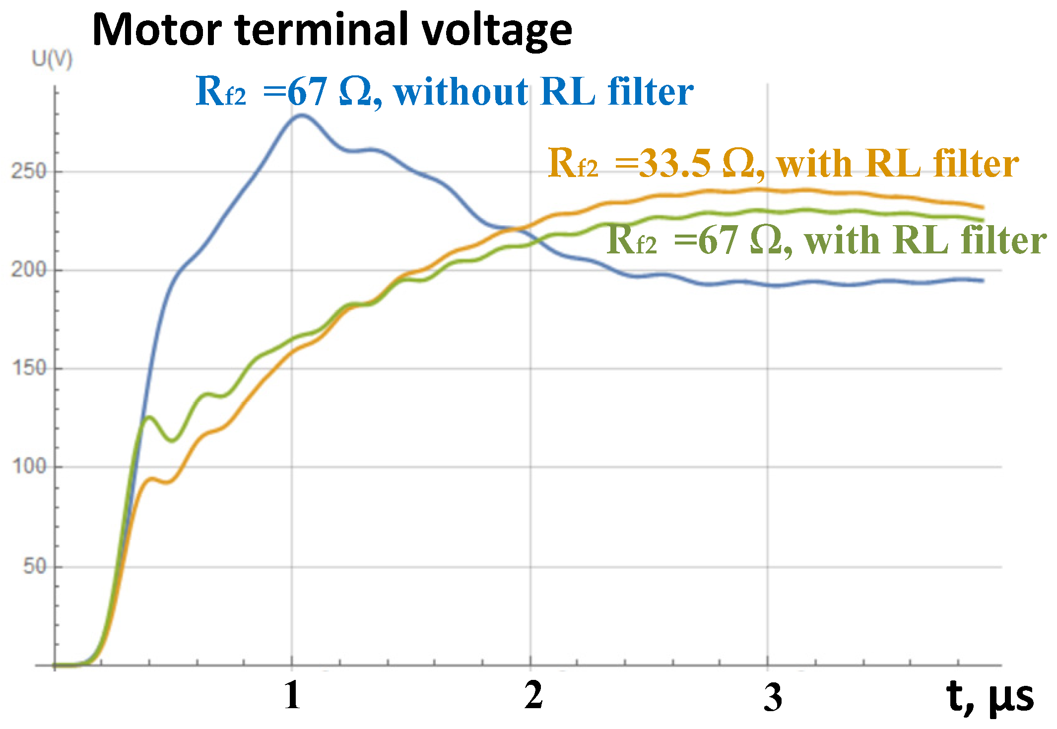
Figure 32, a comparison can be seen between different values of filter resistance
Rf2, with and without RL filter. As can be seen in
Figure 33, the best overvoltage reduction is achieved by combining the RL and RC filters and selecting
Rf2 equal to
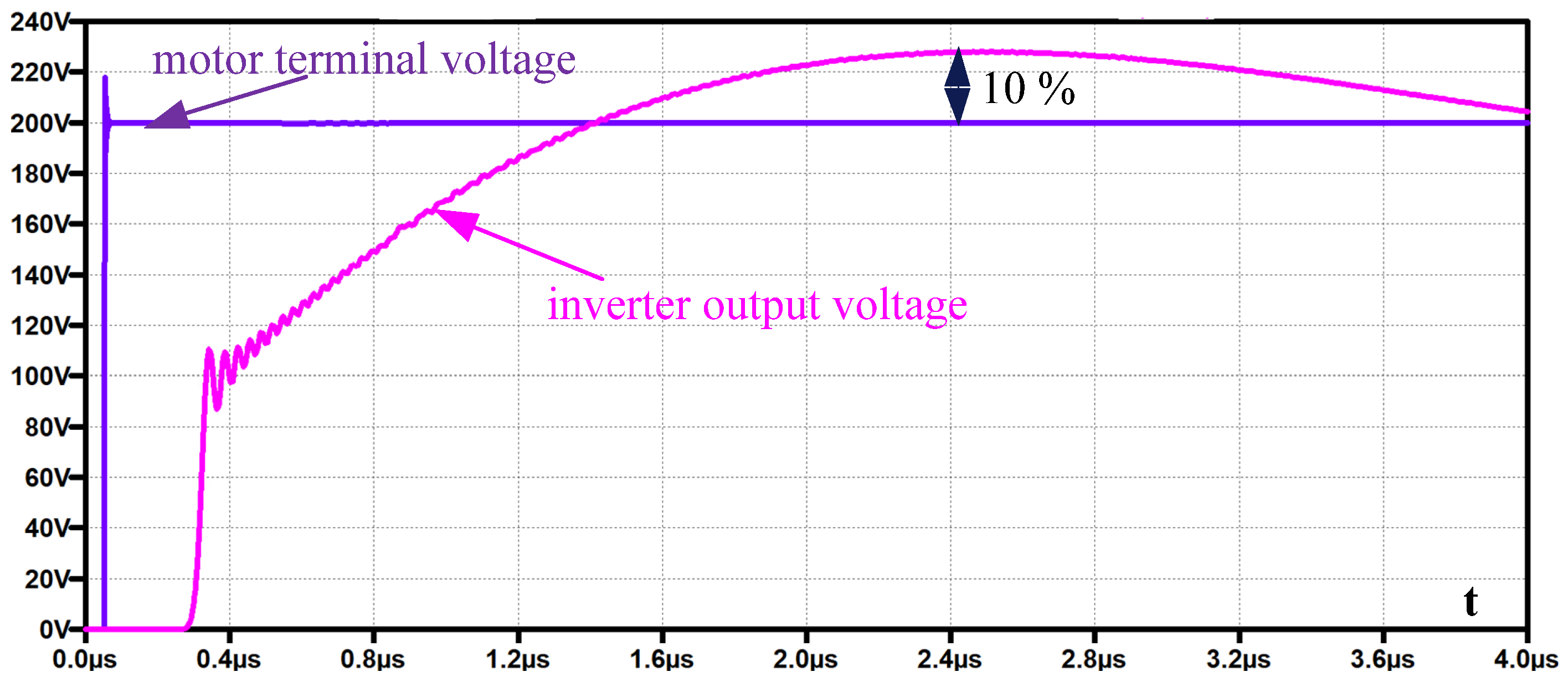
Z0 which, in this case, is 67 Ω. These values were selected as the final solution for implementation.
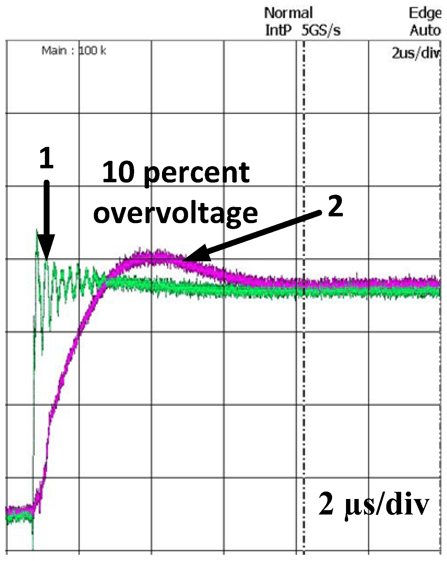
Figure 34 shows experimental results with the improved filter. As can be seen, the overvoltage is small, thus eliminating the problem with high dv/dv caused by the GaN transistor-based inverter. As can be seen, the overvoltage has been reduced to just ten percent. The losses in the case of just the RL filter are 7 W in the case of 50 kHz switching frequency, but in the case of a combination of the RL filter at the input and the RC filter at the input, the losses are 10 W. In the case of higher switching frequency, the losses are going to increase proportionally.
7. Conclusions
Wide bandgap transistors such as GaN transistors have short turn-on and turn-off transition times, thus leading to overvoltage in the cable connecting the inverter and motor. The overvoltage occurs due to reflections in both ends of the cable. The parameters of the high-frequency model of the motor and cable have been determined by measuring the impedance in a wide frequency range. The results shows that the model allows us to accurately determine overvoltage with and without the filtering solution.
Several overvoltage mitigation techniques were experimentally evaluated. The limitation of switching speed of the GaN transistor is an effective solution, but it creates additional losses in the transistor. Since the GaN transistors are small, cooling is not easy, and this solution is preferable only in case the switching speed needs to be limited just slightly. Active filtering is a promising solution, but it is not that easily implementable, since a high-performance control system is required. Traditional passively damped filters remain the most practical and effective solution for most applications. However, conventional RL filters alone are insufficient when dv/dt is very high and cable lengths are long, as they fail to adequately suppress the peak overvoltage.
Therefore, it has been proposed to combine the RL filter with the RC filter connected to the motor terminals. For the selection of filter component values, the equivalent circuit of the cable and motor model has been used, and the electrical circuit of this model has been solved numerically to obtain accurate overvoltage values. Overvoltage is evaluated at different filter values by using numerical solutions and simulations. Results show the effectiveness of the proposed filtering solution. An experimental prototype of the GaN transistor-based three-phase inverter has been built and experiments with a long cable carried out. The experimental result verifies the accuracy of simulation results and results obtained by solving the model circuit numerically. By applying the proposed filter, the overvoltage has been reduced from the initial 80 percent value to 10 percent with losses below 10 W at the 50 kHz switching frequency.
With further development and wider application of wide bandgap semiconductors into motor drives, the problem of overvoltage will have to be addressed more often. Limiting the dv/dt of the transistor is the easiest way but at the same time it reduces benefits from GaN transistor application. The active filter seems to be an effective way to reduce overvoltage, but it requires complex control system and reduces reliability. Therefore, passive filters are still going to play an important role in overvoltage reduction. For proper filter component selection and overvoltage estimation, the high-frequency model of the motor and the cable is important. Complex impedance models do not allow us to obtain equations analytically or even simulate or properly solve circuits numerically. This article has shown that even simplified models can be useful to develop the filter. Further artificial intelligence-based methods to simplify complex high-frequency models and to automate the component selection of the passive filter and topology can lead to more optimal results.