
Article

Is GaN the Enabler of High-Power-Density Converters? An Overview of the Technology, Devices, Circuits, and Applications


by
Paul-Catalin Medinceanu
,
Alexandru Mihai Antonescu
and
Marius Enachescu
*
Department of Devices, Circuits and Architectures, National University of Science and Technology Politehnica Bucharest, 060042 Bucharest, Romania
*
Author to whom correspondence should be addressed.
Electronics 2026, 15(3), 510; https://doi.org/10.3390/electronics15030510
Submission received: 14 December 2025 / Revised: 16 January 2026 / Accepted: 22 January 2026 / Published: 25 January 2026
(This article belongs to the Section Microelectronics)

Abstract

The growing demand for electric vehicles, renewable energy systems, and portable electronics has led to the widespread adoption of power conversion systems. Although advanced structures like the superjunction MOSFET have prolonged the viability of silicon in power applications, maintaining its dominance through cost efficiency, Si-based technology is ultimately constrained by its intrinsic limitations in critical electric fields. To address these constraints, research into wide bandgap semiconductors aims to minimize system footprint while maximizing efficiency. This study reviews the semiconductor landscape, demonstrating why Gallium Nitride (GaN) has emerged as the most promising technology for next-generation power applications. With a critical electric field of 3.75 MV / cm ( 12.5 × higher than Si), GaN facilitates power devices with lower conduction loss and higher frequency capability when compared to their Si counterpart. Furthermore, this paper surveys the GaN ecosystem, ranging from device modeling and packaging to monolithic ICs and switching converter implementations based on discrete transistors. While existing literature primarily focuses on discrete devices, this work addresses the critical gap regarding GaN monolithic integration. It synthesizes key challenges and achievements in the design of GaN integrated circuits, providing a comprehensive review that spans semiconductor technology, monolithic circuit architectures, and system-level applications. Reported data demonstrate monolithic stages reaching 30 m Ω and 25 MHz , exceeding Si performance limits. Additionally, the study reports on high-density hybrid implementations, such as a space-grade POL converter achieving 123.3 kW / L with 90.9 % efficiency.

1. Introduction

Power electronics (PE) has become one of the leading fields in engineering, driven by the ongoing digitization and electrification of modern infrastructure. Power conversion systems (PCS) are found in a wide range of applications, including server farms [1], electric vehicles [2], portable devices, household appliances, and renewable energy systems [3]. The growth of this field is fueled by the demand for higher energy efficiency, reduced system size, and the emergence of new technologies and topologies, such as those discussed in [4,5].
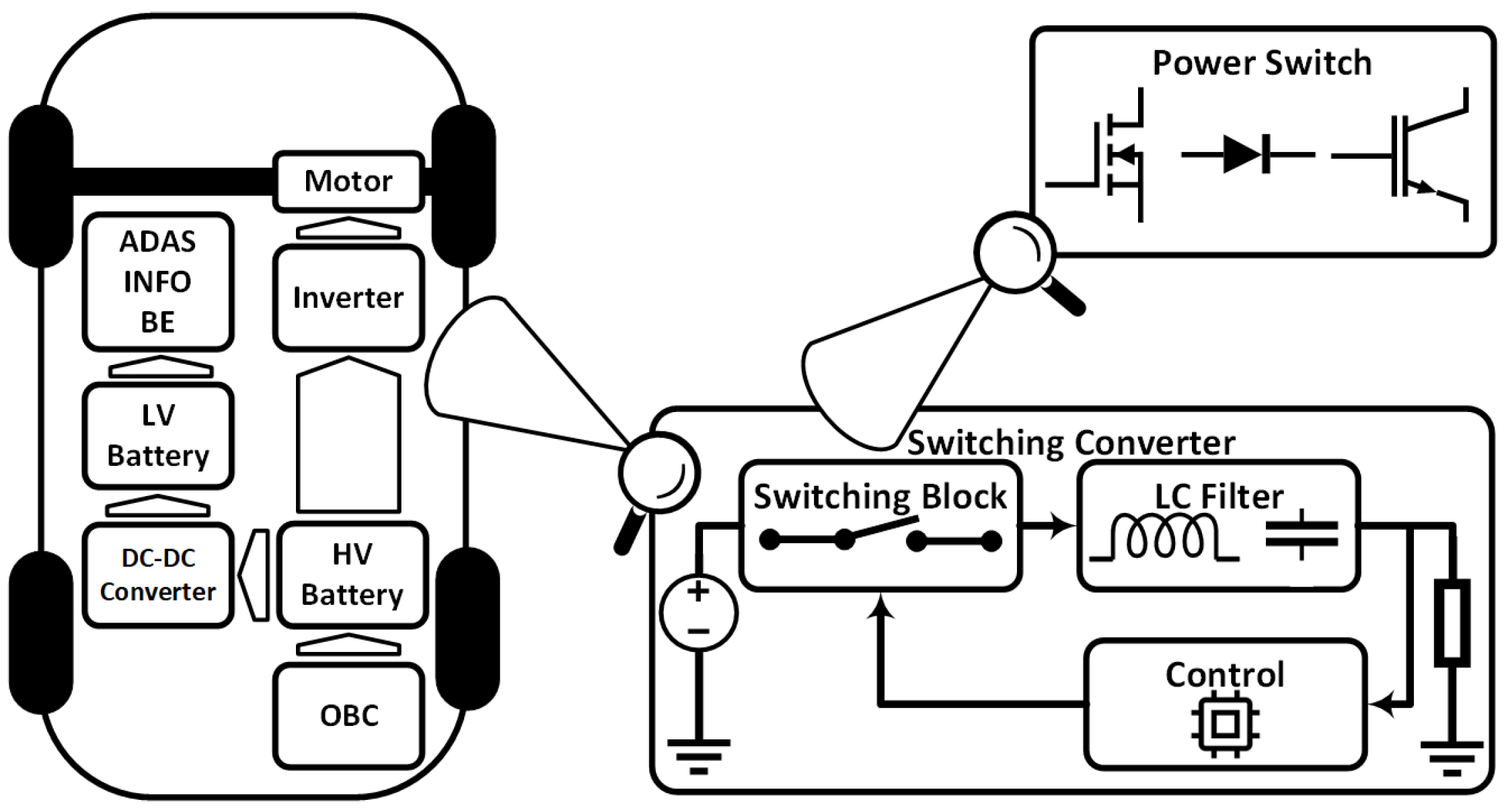
To illustrate the widespread use of power conversion systems, Figure 1 presents the architecture of a fully electric vehicle (EV). In this type of vehicle, two batteries are used: a high-voltage (HV) battery that powers the traction motors, and a low-voltage (LV) battery from which various lower-voltage power buses are derived. The system includes an onboard battery charger (OBC) that enables external charging of the HV battery by converting the grid’s AC voltage into the required HV DC voltage. The LV battery is charged from the HV battery via a DC-DC converter.
As shown in Figure 1, multiple vehicle subsystems are powered from the LV voltage rail. These include body electronics (BE), infotainment systems (INFO), and Advanced Driver Assistance Systems (ADAS). Each of these subsystems may use the LV supply bus to generate its specific required voltages. The electric traction motor is driven by an inverter that converts HV DC power into a three-phase AC voltage. This power architecture clearly demonstrates that numerous power conversions are necessary within such a complex system, with the majority being implemented using various topologies of switching converters (SC).
The lower right side of Figure 1 shows a block diagram of a switching converter (SC). Its main functional components are the control circuit, the switching block (SB), and the output LC filter composed of reactive elements [7]. Among these, the switching block has the most significant impact on the system’s overall efficiency. At its core is the power switch (PS), whose primary role is to control the flow of power through the reactive components. It operates in cycles, alternating between on and off states, driven by square-wave pulse signals generated by the control circuit.
An ideal PS turns on and off instantaneously, exhibits zero resistance when conducting, and blocks any voltage when turned off. In practice, however, PS devices are implemented using semiconductors that introduce several non-idealities, such as conduction resistance ( R o n ), finite switching time, limited drain-to-source breakdown voltage (BV), and, in the case of diodes, a non-zero forward voltage drop [7]. These deviations from ideal behavior result in power losses within the PCS, reducing overall efficiency. Additionally, limitations such as low BV and slow switching speed can restrict the range of applications for a given semiconductor device [8].
Most PSs are implemented using silicon (Si) devices due to their low cost and technological maturity. Si devices have advanced to the point where they can approach, or even surpass, the theoretical R o n and BV limits imposed by the material’s physical properties as presented in [9], through structures such as the IGBT or superjunction MOSFET [10]. At present, the primary commercial competitors for the PS role are Silicon Carbide (SiC) and Gallium Nitride (GaN), both of which are wide bandgap (WBG) semiconductors. Their physical properties translate into higher theoretical material limits, allowing devices to reach higher BVs and lower R o n in the same, or even smaller, device area, whereas many advanced Si structures can approach similar performance only at the cost of significantly larger area [11]. When compared with SiC, GaN transistors allow for higher switching frequencies, primarily driven by their lower parasitic capacitances [12]. The resulting reduction in passive component size contributes to a higher SC power density [13,14], supporting GaN’s growing adoption in portable electronic devices [15,16] as well as in PCS for electric and hybrid vehicles [17] and data-centers [18].
Although multiple overviews and surveys on GaN technology have been published, they typically focus on device design, technology-specific effects, or targeted applications. With the emergence of GaN monolithic integrated circuits, a gap remains in the consolidated discussion of the key achievements and challenges associated with this topic. The scope of this paper is to introduce the challenges in the design of GaN integrated circuits by synthesizing the major advances that have enabled monolithic integration in GaN technology and its resulting benefits, as well as by examining the technology-specific characteristics that impact circuit design. Specifically, this work extends [6] and focuses on three main subjects related to GaN technology: (i) devices, including semiconductor technology, device structures, simulation models, and packaging; (ii) monolithic circuits, covering analog and digital design, power stages, and integrated SCs; and (iii) applications, spanning various application domains and PCS implemented with discrete transistors.
Several semiconducting materials are presented and compared, including Si, GaAs, SiC, and ultra-wide bandgap (UWBG) materials such as Aluminum Nitride (AlN) and β -Gallium Oxide ( β - G a 2 O 3 ). While surveys on WBG technologies have been published [11], this work expands the existing literature by incorporating the physical properties of UWBG semiconductors, as they are expected to play a key role in the future of power electronics [19]. GaN is explored in detail by describing the evolution of the typical power device structure and synthesizing the performance data of various reported power transistors, emphasizing key advantages such as higher BVs in smaller device areas and improved current conduction enabled by ≈1.5× higher electron mobility compared to Si [20]. Additionally, aspects related to the SPICE simulation model and packaging with high thermal efficiency and low parasitic elements are outlined.
Digital circuits represented through different logic gates families [21,22,23,24] and analog circuits, such as amplifiers [25] and comparators [26], are discussed while accounting for technological limitations, such as the absence of complementary devices and significant device parameter variations. Despite these challenges, monolithically integrated circuits, including power stages and integrated SCs, have been developed. GaN power stages can exhibit R o n values as low as 30 mΩ [27] and higher operating frequencies [27,28] compared to Si CMOS implementations [29]. For SCs, despite the technological constraints, control loops have been successfully implemented, enabling system efficiencies exceeding 95% [26,30,31].
A report of performance improvements offered by GaN transistors over their Si counterparts [32] applied to boost converters and a comparative analysis of Si, SiC and GaN devices used in buck converters [33] are used to support that WBG semiconductors are key enablers of the high efficiency and high power density required by emerging power conversion applications. A synthesis of multiple PCS that target fields such as high-performance computing in space [34], aircraft electrification [35] and EVs [36] is presented. These SCs achieve high power densities (e.g., this hybrid point-of-load (POL) [34] converter reaching 123.3 kW / L ) and high power efficiencies (e.g., this three-level flying capacitor multilevel (FCML) converter [36] achieving 98.9%).
The remainder of this paper is organized as follows: Section 2 presents several semiconductor technologies in the context of power applications, emphasizing the physical characteristics that make them suitable for this field. Section 3 focuses on GaN technology, detailing the types of devices fabricated in this process, the simulation model developed for the lateral device, and packaging solutions for emerging technologies. In Section 4, GaN monolithic circuit design is explored, addressing both digital and analog design challenges and summarizing the performance of various power circuits. Section 5 outlines the efficiency gains offered by GaN devices and synthesizes the application areas they have enabled, supported by representative design examples. In Section 6, the authors’ forecast for the development of GaN technology is presented. Finally, Section 7 concludes the paper.

2. Semiconductor Technologies for Power Conversion Applications
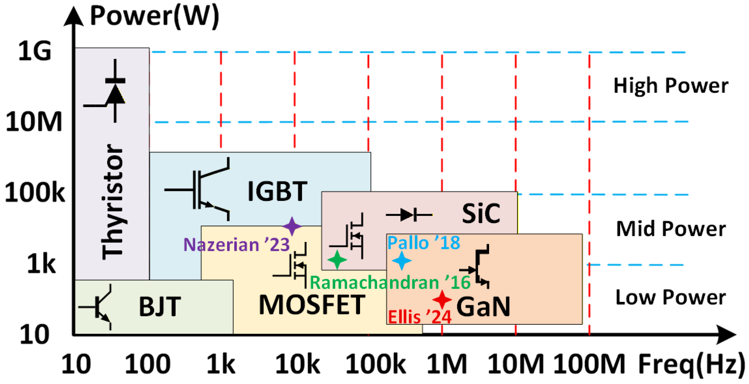
The application’s power rating and switching frequency dictate the choice of semiconductor device [8], as illustrated in Figure 2. For high power applications, Si thyristors are commonly used. In the medium- to high-power range, insulated-gate bipolar transistors (IGBTs) were traditionally the preferred choice. However, with the advent of SiC MOSFETs, the two technologies are now in competition. SiC MOSFETs offer several advantages, including an intrinsic body diode, whereas IGBTs require an external freewheeling diode on the printed circuit board (PCB) or integrated at the package level. Additionally, SiC devices support higher switching frequencies than IGBTs [37]. For low- to medium-power SCs, Si MOSFETs compete with both SiC MOSFETs and GaN High Electron Mobility Transistors (HEMTs). These wide-bandgap devices offer superior performance in terms of voltage-blocking capabilities and switching speed, typically in smaller packages. SiC MOSFETs are favored for their higher BV and thermal conductivity, while GaN HEMTs are preferred for their fast switching capabilities [38].
While several semiconductors are under active research for power electronics, GaN and SiC have already been adopted across a wide range of applications. The technology readiness map from 2023 presented in [39] projects the market shares of SiC and GaN by 2027. According to this forecast, SiC devices are expected to capture approximately 82% of the automotive and transportation market, whereas GaN devices are projected to reach 48% of the consumer electronics market and 31% of the telecommunications market. This distribution is driven by the widespread use of SiC in EV drivetrains and onboard chargers, while GaN has already achieved a dominant position in applications such as USB fast chargers.
Figure 2. Power devices distribution across different power levels and switching frequencies [6]. Comparison based on power and frequency of power device applications from literature by: Ellis’24 [34], Pallo’18 [35], Nazerian’23 [36], and Ramachandran’16 [40]. License Number 6167541103265.
Electronics 15 00510 g002
The feasibility of using emerging WBG semiconductors as PSs stems from their superior physical properties. These materials offer higher critical electric fields, wider bandgaps, greater thermal conductivity, and improved electron mobility. A summary of the physical characteristics of various semiconductor materials is presented in Table 1 [41,42,43,44,45] with key parameters including band gap ( E g ), dielectric constant ( ϵ r ), carrier mobility ( μ n ), critical electric field ( E c ), electron saturation velocity ( v s ), and thermal conductivity (k).
GaAs offers a higher μ n of 8.500 cm 2 V · s compared to Si’s 1.350 cm 2 V · s , making it a preferred material for high-frequency applications such as optical switches and RF devices [41]. However, its low k of 0.5 W cm · K limits its suitability for power applications. SiC, by contrast, is well-suited for high-power and high-voltage applications due to its ≈ 10 × higher thermal conductivity compared to GaAs and about 8 × higher E c than Si. It also serves as a suitable substrate for GaN devices [41]. GaN surpasses all the aforementioned materials in terms of E g and E c , while also exhibiting higher electron mobility than both Si and SiC. As a result, GaN based devices are widely adopted alongside SiC devices in commercial PCS due to their technological maturity and performance [46].
For future power devices, UWBG materials such as AlN, β G a 2 O 3 , and diamond are currently under research [19,42,43,44,45]. As shown in Table 1, β G a 2 O 3 offers promising characteristics compared to GaN, including an ≈2.1× higher E c and ≈1.4× higher E g , which could enable devices with even higher BVs in the future. AlN stands out with the highest E c of 15.9 MV cm among the listed materials, along with a high k of 3.21 W cm · K , surpassed only by SiC and diamond. Among all presented semiconductors, diamond exhibits the best properties, with a ≈3.5× higher μ n , ≈2.7× higher E c , and about ≈18.7× higher k compared to GaN.
Due to its higher μ n , E g and E c compared to Si and SiC; while still being a mature technology unlike UWBG semiconductors, GaN is a strong candidate for implementing PSs. Its material properties allow the fabrication of devices that match or surpass the performance of their Si counterparts while occupying a smaller die area. The reduced device area lowers parasitic capacitances, enabling operation at higher switching frequencies. In turn, this capability supports significant increases in PCS power density, making GaN particularly suited for portable devices, as well as SCs for electric and hybrid vehicles and server farms. For these reasons, GaN technology was selected as the primary focus of this work.

3. GaN Technology

This chapter provides insight into the development of the standard GaN transistor structure and compares various lateral and vertical device implementations. It also covers specific aspects such as the simulation model proposed as the industry standard for this transistor and the packaging methods commonly used for these power devices.

3.1. GaN Devices

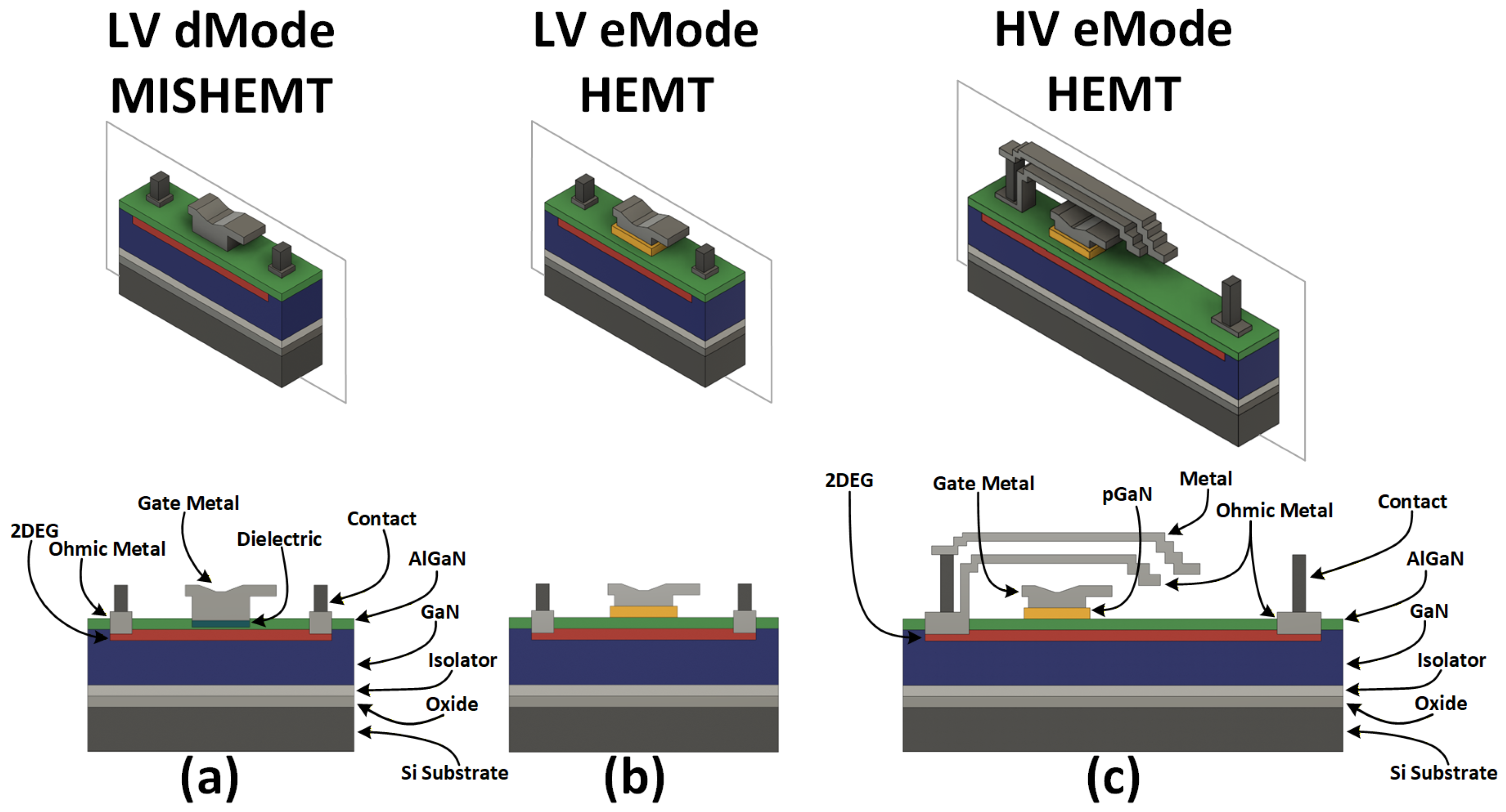
The first GaN transistors utilized a lateral Metal-Insulator-Semiconductor High Electron Mobility Transistor (MIS-HEMT) structure, as shown in Figure 3a. In this implementation, a dielectric layer is inserted between the gate and the two-dimensional electron gas (2DEG) formed at the GaN-AlGaN heterojunction, resulting in a depletion-mode (d-mode) device. In such devices, the channel conducts by default, and electron flow can only be interrupted by applying a negative gate voltage, which repels charge carriers from the channel. Although these transistors offered performance advantages over their Si counterparts, their normally on behavior was considered unsuitable for PE applications due to safety and control concerns. An early commercial solution to this limitation was the GaN-Si cascode structure, which combined a low-voltage Si MOSFET with a high-voltage GaN d-mode HEMT to create a normally off, enhancement-mode (e-mode) configuration [32]. This approach also allowed for the integration of features such as gate driving and protection circuitry within the Si circuit [47].
To eliminate the need for additional components, various device-level modifications have been explored to create e-mode HEMTs. The most widely adopted solution is shown in Figure 3b, where a p-doped GaN layer is introduced beneath the gate. This forms a reverse-biased Schottky junction, which creates a depletion region that suppresses the 2DEG channel under zero gate bias, thereby achieving normally off behavior. To reach BVs in the range of 200 V to 650 V, a HV variant of the device is employed, as depicted in Figure 3c. In this version, the drain region is extended, and field plates are added to redistribute the electric field away from the gate. Another approach to developing devices that leverage the advantages of GaN semiconducting material while exhibiting higher BVs, currents, and reliability than HEMTs is the use of vertical structures such as [49,50].
The p-GaN gate HEMT exhibits a maximum gate breakdown voltage of approximately 7 V, while the recommended gate voltage for achieving low R o n is approximately 6 V. These values leave only a narrow operating margin. As a result, parasitic elements in the gate loop can lead to voltage overshoots, requiring additional PCB-level protection components such as clamps or series gate resistors. To mitigate time-dependent gate breakdown (TDGB), structural enhancements to the device have been proposed in [51], increasing the gate breakdown voltage from 10.5 V to 12.7 V at 25 °C and from 11.4 V to 13.4 V at 150 °C.
While the vertical architectures from [49,50] have successfully demonstrated breakdown voltages exceeding 1.2 kV in compact footprints, they rely on expensive native GaN substrates, which are typically limited to 100 mm diameter wafers. In contrast, utilizing Si substrates for 1.2 kV-rated power switches requires the growth of technologically challenging thick epitaxial layers [52], significantly complicating the fabrication process [53]. To address these manufacturing and cost constraints, industrial research has revisited the GaN–Si cascode topology as a practical interim solution [54,55]. Notably, reference [54] presents a 1.7 kV cascode transistor based on this approach, which has been qualified for automotive and industrial applications and offers a cost-effective alternative to SiC technology.
An initial obstacle that hindered the widespread adoption of GaN devices was the difficulty of growing large GaN crystals suitable for wafer production [41]. The high cost associated with native GaN substrates led to the use of alternative materials such as Si, sapphire, and SiC. Among these, Si is the most cost-effective option, SiC offers improved thermal conductivity at a higher cost, and sapphire is typically used in RF and optoelectronic applications of GaN devices. Recently, a technological breakthrough enabled the production of 300 mm wafers, a development that is expected to reduce GaN device prices in the long term [56].
To mitigate the crystal lattice and thermal expansion coefficient mismatch between the foreign substrates and the GaN/AlGaN layers, a buffer layer is grown between these regions. For clarity, the buffer layer was omitted in Figure 3. An example of a step-graded AlGaN buffer fabrication is shown in [57]. This approach aims to suppress carrier injection into the buffer, which can otherwise lead to punch-through at high blocking voltages. Further improvements in thermal and electrical performance can be achieved by doping the buffer layer with iron or carbon. Such doping increases buffer resistivity, thereby reducing carrier injection [57], and mitigates self-heating effects, which in turn limits drain current degradation caused by low heat dissipation [58].
A milestone in GaN device development is the realization of the dual-gate bidirectional switch (BDS) [59]. This device operates in four modes: it blocks current when both gates are unbiased, functions as a switch when both gates are biased, and acts as a rectifier when only one gate is biased (true for either gate). BDSs are especially useful in SCs such as matrix converters, an AC-AC converter topology that eliminates the need for a DC-link capacitor. Traditionally, the switches in these topologies are implemented using two anti-series connected devices, such as MOSFETs or IGBTs. The GaN BDS offers advantages such as reduced cost, area, and R o n , by utilizing a shared drift region. This innovation has already reached commercial availability [60].
Table 2 synthesizes multiple reported lateral and vertical devices. This GaN fin FET [50] offers ≈24× more current conduction per area and 81 × lower on-resistance compared to the Current Aperture Vertical Electron Transistor (CAVET) reported in [49], while also reducing production cost by eliminating the need for epitaxial regrowth. The transistor reported in [52] exhibits the highest BV among the lateral devices but also an undesirably low threshold voltage of 0.64 V and ≈11× higher R o n than the other works presented. Both Refs. [61,62] HEMTs have very low R o n values of 0.62 m Ω · cm 2 and 0.8 m Ω · cm 2 , respectively. The device in [61] has the advantage of a high BV of 1000 V but suffers from low current conduction. In contrast, the device presented in [62] has a BV of 420 V and boasts the highest current conduction among the HEMTs, reaching 0.86 A/mm. Although [49] has demonstrated the possibility of co-integrating HEMTs and CAVETs, the lateral device structure is still preferred for GaN monolithic circuit design.
In the case of commercial GaN transistors, performance is evaluated not only by current capability, maximum blocking voltage and R o n , but also by the parasitic capacitances ( C i s s , C o s s , C r s s ) and gate charge. For example, this 60 V GaN device [63] rated for 99 A, exhibits a C i s s of 1450 pF, C o s s of 700 pF and C r s s of 17 pF, while achieving an R o n of 1.3 mΩ at a gate voltage of 5 V. When compared to this Si MOSFET from the same manufacturer with the same voltage rating [64], the initial impression may suggest superior performance, as the Si device supports a higher current of 120 A and achieves a lower R o n of 1.1 mΩ. However, this resistance is obtained at a gate voltage of 10 V, and the device exhibits larger parasitic capacitances: 6× higher for C i s s , ≈2× higher for C o s s and ≈3.5× higher for C r s s . These increased capacitances, together with the higher gate drive voltage requirement, lead to increased switching and driver losses and limit operation at high switching frequencies. A further advantage of the GaN device in this comparison is its smaller PCB footprint, occupying approximately half the area of the Si MOSFET.
Additionally, owing to the high bond strength of the material, GaN transistors exhibit promising characteristics for aerospace applications [65]. Because high energy is required to create lattice displacements, GaN is considered inherently radiation hardened; however, this property also depends on device design and material quality. The primary radiation effects observed in semiconductor devices include total ionizing dose (TID), displacement damage, and single-event effects (SEEs) [66]. In the case of p-GaN gate devices, threshold voltage shifts due to TID have been reported to be negligible after exposure to a total gamma dose of 1 Mrad (Si) [67]. Furthermore, due to the absence of a gate oxide, GaN HEMTs are expected to exhibit high immunity to TID effects. In [68], the displacement damage effects for a p-AlGaN gate device were investigated. Since many satellites and space stations operate in low Earth orbit, where protons are the dominant source of radiation, the device was irradiated with protons at an energy of 5 MeV. Following irradiation, the device R o n increased from 1.89 mΩ to 5.29 mΩ, while the drain current was reduced by 50%. After thermal annealing at 400 °C, the device characteristics exhibited partial recovery. SEEs are of particular concern in power systems due to their potential to cause device degradation or catastrophic failure. SEEs occur when a high-energy radiation particle strikes a device, generating a track of electron-hole pairs that can induce transient disturbances, permanent parametric shifts, or instantaneous failure. In [69,70], commercial GaN transistors were subjected to irradiation, and their electrical characteristics were evaluated following SEE exposure. In both studies, high breakdown-voltage devices exhibited increased gate and drain leakage currents after irradiation. By contrast, the 40 V device reported in [69] showed lower charge amplification compared to the 100 V and 200 V devices, and no SEE-induced failure was observed for this device. While GaN technology is still under active investigation for space applications, it shows potential, as evidenced by the release of radiation-hardened GaN products specifically targeting this domain [71,72].

3.2. GaN HEMT Model

Due to the structure of GaN transistors and the material-specific properties of GaN technology, standard SPICE models are inadequate for accurately capturing device behavior. The authors of [73] highlight key differences between MOSFET and HEMT devices, including significantly different transfer characteristics and a threshold voltage that exhibits weak temperature dependence in GaN HEMTs. To better reproduce the characteristics of HEMTs in circuit simulations, two main modeling approaches can be identified: a top-down approach, in which the device behavior is characterized and represented using implementations built from available SPICE devices or look-up tables, and a bottom-up approach, in which a physics-based compact model is developed.
In [74], the GaN transistor modeling using standard SPICE devices was investigated for a synchronous Buck converter. Although the simulated efficiency matched the measured results with an error of approximately 1%, this approach does not account for device-specific physical effects that can influence efficiency under practical operating conditions. Furthermore, empirical models based on fitting parameters or table-based representations become unreliable when extrapolated beyond the measured bias range.
To overcome these limitations, two industry-standard physics based models have been proposed: the Advanced SPICE Model for GaN HEMTs (ASM-HEMT), which is based on surface-potential calculations [75], and the MIT Virtual Source GaN-HEMT (MVSG) model, which is based on charge-based formulations [76].
In [75], HEMT-specific features incorporated in the ASM-HEMT model, such as access region resistance and field plates, are described. Its accuracy was validated by comparing simulation results with measured data for both RF and power devices. The same model was applied in [77] to a GaN–Si cascode PS, where it accurately reproduces device capacitance behavior while accounting for the effects of field plates.
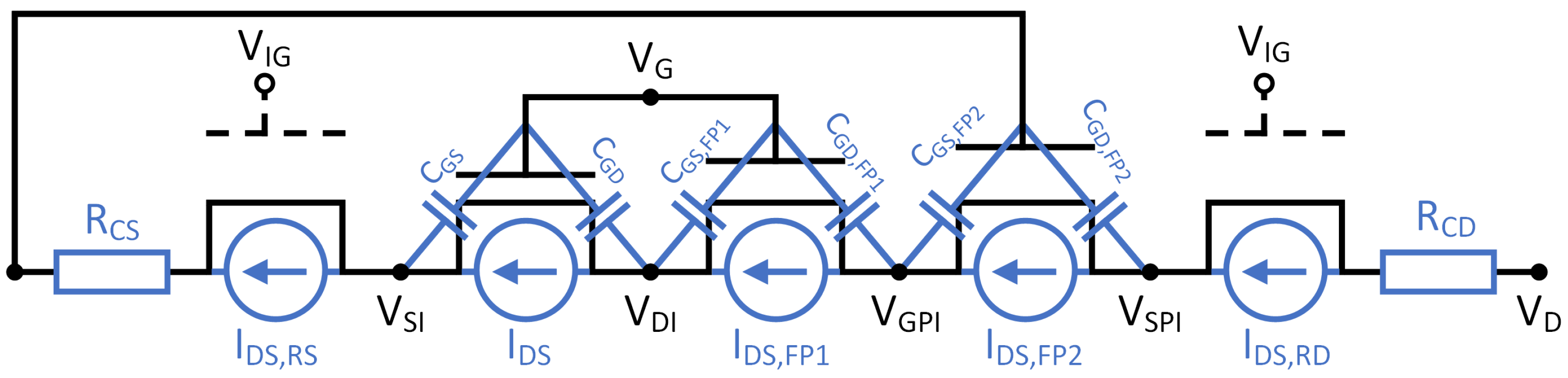
The MVSG model presented in [78] employs a charge-based approach that simplifies the model formulation compared to ASM-HEMT, while maintaining numerical robustness. Its equivalent circuit is shown in Figure 4. The schematic illustrates five distinct regions of the device: the intrinsic transistor region under the gate, two field plate regions on the drain side that enhance the BV, and two access regions at the ends of the channel, modeled as implicit gate (gate voltage is V I G on the schematic) transistors. The superimposed components in blue represent the modeled elements that define the device behavior. These components, implemented in Verilog-A, include: resistors modeling contact resistance; C G S and C G D modeling the gate-source and gate-drain capacitances; and C G S , F P 1 , C G D , F P 1 , C G S , F P 2 , and C G D , F P 2 modeling the capacitances between each field plate and the source or drain.
This model accounts for phenomena such as access-region depletion, dynamic thermal behavior, and charge-trapping effects. Its accuracy was validated through simulations of an HV Buck SC and an RF power amplifier. In the Buck converter case, the model accurately predicted the slew rate of the half-bridge switching node, demonstrating its effectiveness in capturing transient behavior. Further enhancements to the MVSG model have been proposed to include the behavior of the Schottky p-GaN gate. The validity and accuracy of this extension were confirmed through comparisons with experimental data and TCAD simulations [79].
Although the charge trapping effect has been incorporated into various modeling approaches, its accurate measurement remains challenging, as it depends on factors such as blocking voltage, pulse duration, and temperature. This phenomenon leads to a dynamic R o n , which manifests as a temporary increase in conduction resistance following the blocking of a high drain voltage. An on-wafer double-pulse test method for this purpose is proposed in [80]. The ability to characterize devices before dicing is a valuable and time-saving feature, enabling faster design iterations during device development. In [81], device characterization and SPICE modeling methodologies for charge trapping are presented. Although the proposed approach relies on fitted parameters, the model that includes the dynamic R o n effect exhibits a maximum error of 22.4%, whereas the model without this feature shows an error of 86.9% when comparing simulated and measured R o n values.

3.3. GaN Packaging

The power losses in a PCS are converted into heat, which must be effectively dissipated to ensure reliable operation. As the temperature rises, the R o n of power transistors increases, leading to even greater power losses. Additionally, excessive temperatures can cause irreversible damage to the device, making thermal management a critical aspect of PCS design. While WBG devices deliver superior performance in smaller die areas, this miniaturization inherently limits heat dissipation. These thermal challenges are further intensified by the demand for higher system power densities and reduced PCB footprints, necessitating cooling solutions that do not compromise miniaturization.
To meet these requirements, chip-scale (CS) packages have been adopted for GaN devices [82]. This packaging style improves the package-to-die size ratio, reducing overall packaging costs, which helps compensate for the higher material costs of GaN, and enhances thermal performance by eliminating additional thermal impedances introduced by traditional package methods.
In [83], the thermal performance of commercial chip-scale GaN power transistors was compared to that of Si power MOSFETs housed in various packages. To ensure a fair comparison between the two technologies, Buck converters were developed using each device. When comparing a GaN HEMT to a MOSFET in a CanPAK package, both operating without additional cooling and under a 30 A load, the GaN-based system demonstrated a 35% reduction in power losses at a switching frequency of 300 kHz, and a 40% reduction at 400 kHz. When equipped with a heatsink, the SC using GaN achieves an output current of 30 A while operating at 100 °C, whereas its Si counterpart is limited to 20 A under the same thermal conditions. As a result, the GaN-based system delivers 50% higher output power at the same temperature.
Another advantage of CS packaging is the reduction in parasitic resistance and inductance. Thanks to the lateral structure of GaN HEMTs, there is no need for leadframes or bond wires to bring the drain, source, and gate terminals to the same plane. In contrast, Si power transistors typically use vertical structures, which place the drain and source on opposite sides of the die, requiring such interconnections. The reduced parasitic resistance helps further decrease R o n , while the lower parasitic inductance enables higher switching frequencies with minimized voltage ringing. Reduced ringing, particularly on the gate signal, is crucial, as excessive oscillation can damage the gate terminal [84].
While CS packaging improves the electrical performance of the device, it also presents disadvantages related to thermal management, as the limited area available for heat dissipation can lead to increased thermal stress. High operating currents may induce mechanical strain in solder bumps or even cause chip damage. For flip-chip packages, the influence of solder bump material and packaging method has been investigated through simulation in [85]. The results show that, due to its smaller size, the CS package experiences higher mechanical stress compared to a die directly attached to a copper substrate. Two solder bump materials, copper and aluminum, were evaluated, with aluminum exhibiting lower package stress under repeated temperature cycling. These simulation results are supported by measurements reported in [86], where a switching converter exhibits reduced efficiency at high load currents when employing a flip-chip packaged GaN IC.
Ongoing research focuses on advancing packaging methods for emerging semiconductor technologies. In [87], the authors propose replacing traditional bond wires with copper clips and sintered copper paste to improve thermal and electrical performance. Meanwhile, [88] explores embedding the GaN die directly into the PCB and positioning the decoupling capacitor as close as possible to the die, significantly reducing parasitic inductance. These findings highlight that advanced packaging techniques are essential for emerging power semiconductor technologies to minimize parasitic elements and enhance thermal conductivity. Despite its disadvantages, chip-scale packaging is currently the most prevalent solution, as it enhances performance by reducing thermal impedance and parasitic elements. This is achieved through the use of redistribution layers combined with solder bumps or copper pillars, which lower parasitic resistance and inductance while also providing an additional path for heat dissipation.

4. GaN Monolithic Integrated Circuits

The high switching frequencies targeted by GaN devices pose a challenge due to the parasitic inductances inherent in the packaging, bond wires and PCB traces. Such phenomena can induce voltage ringing on the gate of GaN power transistors, potentially leading to destructive overshoot. To address this issue, the first approach was to package GaN HEMTs with Si gate drivers to minimize parasitics. To further reduce these inductances, monolithic integration of the control circuits and power transistor has emerged as a solution [20]. This chapter presents the adopted digital and analog design techniques used in this technology and reports and compares the performances of multiple GaN monolithic circuits.

4.1. Digital Design

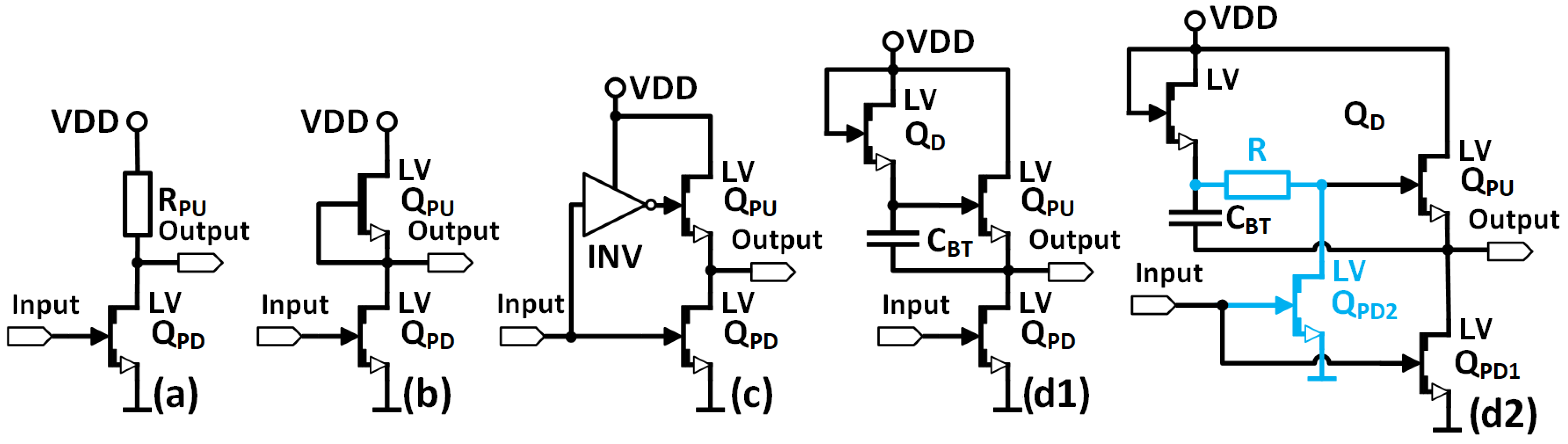
The initial step in developing GaN ICs involves designing suitable digital circuits. Since commercial technologies lack a p-type GaN device, primarily due to the added fabrication complexity and the 50 ÷ 100 times lower transconductance [20], alternative logic families have been developed to overcome this limitation. These logic families primarily differ in their implementation of the pull-up (PU) network. The main types of logic families used in GaN ICs are presented in Figure 5 and respecting the notation from the figure they are described as follows: (a) Resistor-Transistor Logic (RTL): In this family, the load is a resistor [21], (b) Direct-Coupled FET Logic (DCFL): Here, the PU is a d-mode GaN device [22], (c) Pseudo-Complementary FET Logic (PCFL): In this family, the load is an e-mode device controlled by a signal complementary to the input, resembling a push-pull stage [23], (d1) Bootstrapped (BS) Logic: This logic family uses an enhancement-mode device as the PU, with its gate bootstrapped through a diode and a capacitor [24]. Due to its complementary control, the PCFL family has the lowest power consumption, while the BS family exhibits better noise margins with smaller devices when compared to DCFL [24]. Additionally, the enhancements to the BS logic family proposed in [89] are illustrated in Figure 5(d2), and consist of the addition of a PD device and a resistor (highlighted in blue), which effectively reduce static current. However, this modification results in a slower rise time.
Even though the complementary GaN device demonstrates inferior performance compared to its n-type counterpart, novel approaches for its utilization have been proposed, such as in [90]. In this work, the complementary device is employed to block leakage current paths and reduce static power consumption. Moreover, the use of this hybrid topology leads to improvements in both fan-out and propagation delay.
When considered in the context of digital design in other IC technologies, commercially available GaN processes lead to logic families that resemble earlier solutions developed in Si NMOS/PMOS, Si BJT, or GaAs technologies. For example, processes that provide only e-mode devices may employ RTL style loads, BS loads, switched e-mode devices as dynamic loads, or biased e-mode devices operating in the linear or saturation region as active loads. In processes that include both e-mode and d-mode devices, DCFL can be implemented, which corresponds to ratioed logic in NMOS or PMOS technologies. Furthermore, when Schottky diodes are available, logic gates analogous to bipolar diode–transistor logic (DTL) or GaAs-style logic families can be realized [91,92,93].

4.2. Analog Design

Power stages and switching regulators often incorporate protection circuits, such as overtemperature, overcurrent, and overvoltage protection, which are typically implemented using analog blocks. Furthermore, as demonstrated in [26,30,31], control loops in SCs are also realized using analog techniques.
One challenge in GaN analog design stems from the absence of p-type devices. The lack of complementary transistors imposes several constraints: it necessitates the use of resistors as loads, limits current mirrors to sinking-only configurations, and restricts the input common-mode range of differential pairs. Given the p-type current mirrors unavailability, large-area resistors are used as loads when designing GaN-based amplifiers. As shown in [25], with only 20 dB per amplification stage, multiple stages of differential amplification are required to achieve a gain of 60 dB. A similar cascading approach is used in the comparator of the Buck converter presented in [26], where two amplifier stages are employed to attain a gain of 31 dB.
The common-mode limitation of e-mode n-type-only GaN technologies comes from the high positive threshold voltage of the devices. As a result, input signals below this threshold require level shifting. Two solutions have been proposed: in [26], diode-connected HEMTs are used in the comparator to shift the input voltage levels, whereas in [30], a switched-capacitor technique is employed for level shifting.
Crystal defects in GaN degrade device matching, imposing an additional constraint on analog design. In [20], the matching performance of various fundamental analog building blocks was evaluated. A resistive divider demonstrated a mismatch standard deviation of σ = 0.76 % between its resistors and an absolute resistance variation of σ = 10.9 % across the wafer. These resistors are implemented using 2DEG channels formed from HEMTs without gates. However, due to back-gating effects in the upper device, its resistance is consistently higher than that of the lower device. Threshold voltage measurements reported in [32] show that standard HEMT structures exhibit a variation of σ = 229 mV, whereas structures with a modified gate reduce this variation to σ = 63 mV. These mismatches significantly impact analog circuits, especially differential pairs, resulting in input-referred offsets as high as ± 200 mV .
A solution to mismatches in current mirrors is the use of source degeneration, as resistors are expected to exhibit less variation compared to HEMTs due to the absence of the layers required to form the p-GaN gate [20]. This approach has been implemented in the level shifter of the power stage described in [94], although no data is reported regarding the accuracy of current matching. To address mismatch in differential stages, auto-zeroing and chopping techniques can be applied, as demonstrated in the comparator from [95], which successfully reduces the input offset from 112 mV to 1.2 mV.
Another physical effect observed in GaN e-mode HEMTs that can affect analog performance is positive bias temperature instability (PBTI), which manifests as a shift in the threshold voltage following positive gate-bias stress [96]. This effect results in hysteresis in the device transfer characteristics. Its impact has been investigated in the context of a comparator in [97], where it caused a shift in the input voltage at which the output transitions from logic high to logic low.
Similarly to digital design, analog circuit design in GaN technologies largely borrows from earlier approaches developed for NMOS and GaAs processes. For instance, the input stage of the GaN comparator presented in [98] resembles the architecture used in the GaAs comparator reported in [99]. A key difference between the two implementations is that the GaN circuit uses a resistor to bias the differential pair, whereas the GaAs design employs a depletion-mode device as a tail current source. A similar trend can be observed in operational amplifier design: although more complex, the GaN implementation reported in [100] adopts circuit techniques analogous to those used in earlier NMOS designs such as [101]. To date, experimental analog circuits based on truly complementary GaN devices have not been reported.

4.3. Power Circuits

To overcome the limitations imposed by parasitic inductance on the switching frequency of GaN transistors, monolithic integration of the driver and the PSs on a single die has been adopted, resulting in a power stage circuit. Various research implementations of such circuits are enabled by one or more of the previously discussed logic families. For example, the GaN half-bridge circuit in [94] employs a combination of RTL and PCFL, while the design in [21] exclusively uses RTL gates. Additionally, the commercial GaN IC presented in [102] is based on the BS logic gates family.
The characteristics of multiple power stages are summarized in Table 3. The IC detailed in [29] exhibits the slowest switching frequency and the highest R o n , serving as a reference Si power stage. The multi-die approach from [103], which combines Si control with GaN PSs, stands out among the listed circuits by achieving the lowest R o n at 4.4 m Ω , the highest drain current of 35 A, and the second-highest switching frequency of 10 MHz.
The power stage presented in [27] integrates switches with an R o n of 30 m Ω , the second-lowest value in the table, and supports a high switching frequency of 25 MHz. The design utilizes the modified BS logic gate family shown in Figure 5(d2) to enhance PU speed and reduce static power consumption. While it results in higher power consumption at lower frequencies, it achieves lower power consumption in the 25–30 MHz range compared to a commercial Si driver. It also features a level shifter with high common-mode transient immunity, as well as an adaptive PD switch that prevents signal loss during freewheeling. The circuit presented in [104] employs a segmented, binary-weighted driver to control the voltage slopes of the gate and drain terminals. This approach effectively reduces gate voltage oscillations, thereby preventing the potential damage of this terminal. The power stage presented in [28] exhibits the highest dynamic power loss, due to its RTL driver implementation. Although this work does not propose a complex design, it compares the circuit’s performance with simulation results based on the MVSG model for the HV device, showing a maximum error of 21.2% in the t O N switching time parameter. In [94], a novel protection method for the high-side latch in the level shifter is proposed. The drivers are implemented using RTL gates that control two push-pull stages in a PCFL configuration, reducing power consumption in the stages with higher output current capability. Two different supply voltages are used to configure the resistance of the PU devices and mitigate voltage overshoots at the gates of the PSs. The commercial circuit in [102] employs the BS logic family and is the only GaN power stage that integrates a bootstrap switch for the high-side driver; all other implementations use an external diode. It supports a maximum operating current of 40 mA at 3 MHz, while the BS power stage from [27] achieves a current consumption of 20 mA at 5 MHz. The circuit also includes an undervoltage lockout block that enables operation only when the supply voltage exceeds a specified threshold.
Another promising type of power circuit for GaN monolithic integration is the switching regulator, which is a system that incorporates a power stage and a control loop. Multiple Buck SCs have been reported [26,30,31].
The circuit presented in [30] is realized in an e-mode 650 V GaN technology, occupies an area of 2.1 mm 2 and achieves an efficiency of 95.6% for an input of 85 V. The control loop operates in boundary conduction mode. It integrates a zero voltage detector (ZVD) and reads the output current through a shunt resistor. When the switching node reaches zero volts, the driver control signal is set high, and when the current reaches a peak value determined by an external voltage reference, the signal is set low. This way, the average current is set by the reference voltage.
A GaN buck converter for server POL applications is proposed in [31]. It is designed in a 200 V GaN-on-SOI technology, and for a load of 3 A and a switching frequency of 250 kHz, it achieves an efficiency of 84.3% when stepping down from 48 V to 1 V. The integrated feedback loop employs voltage mode control.
In this work [26], a SC fabricated in a 650 V GaN technology is presented. The circuit converts from 400 V to 48 V, occupies an area of 16.25 mm 2 , and achieves an efficiency of 93.1%. A peak efficiency of 95.5% is reached when stepping down from 250 V to 125 V. The converter employs a constant-on-time (COT) control method and integrates a ZVD, which enables soft switching of the low-side transistor. Using this circuit, a 5.5% efficiency improvement is reported compared to operation with the ZVD disabled. The minimum on and off times of the control loop are trimmed using 5-bit and 3-bit resolution, respectively, through adjustment of a binary-weighted capacitor bank. The power stage can operate at frequencies up to 3.5 MHz, but the COT controller is capable of generating control signals only up to 1.7 MHz.

5. GaN Power Converters Evaluation

This section presents a synthesis of reported efficiency improvements in PCS driven by replacing Si devices with GaN HEMTs, complemented by a review of SCs architectures designed to maximize power density using this technology.
In [32], the authors evaluate the performance improvements offered by GaN transistors over their Si counterparts in Boost converters, considering both non-synchronous and synchronous topologies. While the Si-based non-synchronous converter reaches a peak efficiency of 98.2% at 500 kHz, the GaN implementation demonstrates superior performance, achieving 98.5% peak efficiency and maintaining a flatter efficiency curve at heavier loads. Similarly, in the synchronous Boost topology operating at 100 kHz, the synchronous Boost converter with Si switches was limited to 2.4 kW output due to thermal constraints, peaking at 97% efficiency. The GaN-based equivalent, however, delivered 37.5% more power and maintained 99% efficiency across a 1.4 kW to 2.9 kW load range.
The comprehensive comparative analysis presented in [33] evaluates Si, SiC, and GaN implementations within a synchronous Buck converter topology, operating with an input range of 140–240 V and a 48 V output. The goal was to identify the optimal device technology for maximizing both efficiency and power density. Three configurations were analyzed: Si MOSFET and diode, SiC JFET with SiC Schottky diode, and GaN transistor paired with SiC Schottky diode. The results show that, across the full input voltage range, the hybrid GaN-transistor/SiC-Schottky implementation achieved the highest performance, with peak efficiencies of ≈97% at 100 kHz and ≈96% at 200 kHz. It was closely followed by the SiC-JFET/SiC-Schottky combination, which reached about ≈96.5% and ≈96% at the same frequencies. In contrast, the Si-based implementation achieved only around ≈90% efficiency at 100 kHz and dropped to ≈82% at 200 kHz.
Synthesizing the findings from the aforementioned studies [32,33], it confirms that GaN and other WBG semiconductors are key enablers for attaining the high efficiency and power density demanded by emerging power conversion applications. Multiple SC implementations using discrete GaN devices that meet these demands are synthesized in Table 4. These systems target applications such as power delivery systems for high performance computing in space [34], aircraft electrification [35] and EVs [36]. Moreover, these PCSs are represented in Figure 2 as a function of output power and switching frequency, placing them within the broader context of the power semiconductor landscape.
In [34], the authors present a high conversion rate POL converter developed for space applications, enabled by GaN’s inherent radiation hardening. The design can output a maximum of 50 A at ≈86% efficiency while keeping a steady temperature of 58 °C under forced air cooling. The reported peak system efficiency is 90.1%.
The inverter developed in [35] targets aircraft electrification. A FCML topology was selected to reduce both power loss and system weight. Through this architecture, although the switching frequency is 120 kHz, the effective ripple frequency at the inductor input reaches 960 kHz, allowing the use of two 10 μH inductors that occupy less PCB area. The system achieves the second-highest power density among the surveyed works at 35.3 kW/L, while reaching a peak efficiency of 98.6%.
The isolated bidirectional converter presented in [40] achieves a peak efficiency of 98.8% in both buck and boost modes. To further improve system efficiency, the authors designed custom wound inductors and a transformer for the prototype. Although the converter height is not reported, preventing a precise power-density calculation, the prototype delivers 1.7 kW of power while occupying a PCB footprint of 14.3 cm × 7.7 cm.
An FCML topology is also employed in the DC–DC SC presented in [36] for EV applications. Similarly to the FCML inverter in [35], this architecture results in the inductor input being switched at twice the fundamental switching frequency, enabling a reduction in inductor size. This converter exhibits the highest inductor size and lowest power density, with a value of 16.54 kW/L, but has a high output power target of 10 kW, while also having the highest input and output voltages from the selected papers.
Beyond the already mentioned applications, GaN-based converters are now used in satellites, augmented-reality systems, and robotics [32]. A common thread across these fields is the need for small footprint and energy-efficient power conversion: portability implies battery operation and strict space and thermal constraints, as in robotics and drones [106], while satellites require compact electronic systems with radiation tolerance [107].
Driven by the inherent advantages of monolithic integration discussed in Section 4, together with the demonstrated superiority of discrete GaN transistors over their Si counterparts highlighted in this section, single chip GaN power integrated systems represent an important milestone in the evolution of the technology, with commercial products already available [102,108].

6. Discussions

The author’s forecast for the development of GaN technology is outlined in the following paragraphs. In the case of discrete devices, the advancement of 300 mm GaN wafers is expected to enable the fabrication of vertical devices capable of withstanding BVs exceeding 1200 V. These devices will compete with IGBTs and SiC-based components, positioning GaN technology within the mid- to high-power range of the power semiconductor spectrum.
For IC technologies, GaN-based solutions are anticipated to incorporate a broader variety of devices, including fuse elements, which would allow on-chip parameter calibration directly within the power stage, eliminating the need for external Si-based circuitry. Device structures will be optimized for both cost and electrical performance, with particular attention to parameter variation and manufacturing yield. Furthermore, as reported by Intel in [109], hybrid integration of Si and GaN is feasible, suggesting that growing HEMT power devices directly on a Si driver could become a practical approach.
At present, monolithic GaN power stages have gained traction in portable applications such as chargers, drones, and robots. However, wider adoption is anticipated in data center servers and in hybrid or fully electric vehicles, particularly for DC-DC converters between the system’s HV and LV batteries. Upon the commercial release of devices with a BV of 1200 V, GaN is expected to be adopted in traction inverters and OBCs as well.
Due to the small form factor of GaN devices and the benefit of enabling smaller reactive components, we can expect to see a rise in compact system-in-package (SiP) designs. Regarding packaging, CS packages are widely used across semiconductor technologies due to their low cost, small footprint, reduced parasitics, and good thermal conduction. Thermal performance can be enhanced by adding thermal pads that facilitate the attachment of heat sinks. A potential implementation has been investigated in [110], where the backside of the die is removed to allow filling with a high thermal conductivity material, such as copper. A similar approach was investigated in [111], where backside copper filling resulted in a temperature reduction of 22 °C. This reduction mitigated self-heating effects and led to a 26% improvement in the transconductance of the HEMT. This technique could be applied to both SiPs mounted on PCBs and chips employing CS packaging.

7. Conclusions

This paper presented the need for efficient, high-power-density PCS. It showed that, while Si is currently used across a wide range of power applications, its performance is fundamentally limited by its physical properties. As alternatives, several semiconductor technologies were discussed, including WBG and UWB materials, with a focus on GaN. By reviewing key advancements in GaN technology, spanning fabrication processes, device design, compact modeling, packaging, circuit implementation, and converter architectures, this work demonstrated its suitability for next-generation power electronics. Through its high switching frequency, small footprint, and low R o n , GaN technology has been shown to meet the demands for high efficiency and power density in applications such as portable chargers, electric vehicles, and satellites. This was supported by reported performance examples, such as a monolithically integrated GaN buck converter achieving 95.4% peak efficiency when stepping down from 250 V to 150 V, and a synchronous boost converter using discrete GaN transistors, which delivered 37.5% more power while maintaining 99% efficiency. GaN devices have also enabled switching regulators for fields such as high-performance computing in space and aircraft electrification, and have improved the feasibility and cost-effectiveness of topologies like the matrix converter. Thus, GaN power devices, through their superior physical properties, have surpassed Si in low- to mid-power applications. With continued technological advancements, GaN could compete with SiC in the mid- to high-power range and approach its theoretical limits, eventually to be surpassed by emerging UWBG materials.

Author Contributions

For this review article, P.-C.M. was responsible for the ideation, literature search, and data analysis; A.M.A. conducted the literature search and synthesis for Section 3.2 and Section 3.3; and M.E. was responsible for supervision, and for drafting and revising the manuscript. All authors have read and agreed to the published version of the manuscript.

Funding

This work was funded from the project “National Platform for Semiconductor Technologies” Contract no. G 2024-85828/390008/27.11.2024, SMIS Code 351364, funded by the European Regional Development Fund under the Operational Program for Smart Growth, Digitization and Financial Instruments (POCIDIF), Priority 4—Development of Strategic Technologies for Europe—STEP.

Data Availability Statement

The original contributions presented in this study are included in the article. Further inquiries can be directed to the corresponding author(s).

Conflicts of Interest

The authors declare no conflict of interest. The funders had no role in the design of the study; in the collection, analyses, or interpretation of data; in the writing of the manuscript, or in the decision to publish the results.

Abbreviations

The following abbreviations are used in this manuscript:
ADASAdvanced Driver Assistance Systems
AlNAluminum Nitride
BDSBidirectional Switch
BEBody Electronics
BSBootstrapped
BVBreakdown Voltage
CAVETCurrent Aperture Vertical Electron Transistor
COTConstant-On-Time
CSChip-scale
DCFLDirect-Coupled FET Logic
DTLDiode-Transistor Logic
EVElectric Vehicle
FCMLFlying Capacitor Multilevel
GaAsGallium Arsenide
GaNGallium Nitride
HEMTsHigh Electron Mobility Transistors
HVHigh Voltage
ICIntegrated Circuit
IGBTInsulated Gate Bipolar Transistor
INFOInfotainment
LVLow Voltage
MIS-HEMTMetal-Insulator-Semiconductor HEMT
MVSGMIT Virtual Source GaN-HEMT
OBCOnboard Battery Charger
PCBPrinted Circuit Board
PCFLPseudo-Complementary FET Logic
PCSPower Conversion System
PDPull-Down
PEPower electronics
POLPoint-Of-Load
PSPower Switch
PUPull-Up
RTLResistor-Transistor Logic
RFRadio Frequency
SCSwitching Converter
SBSwitching Block
SEESingle-event Effect
SiSilicone
SiCSilicone Carbide
SiPSystem in Package
TIDTotal Ionizing Dose
UWBGUltra Wide Bandgap
WBGWide Bandgap
ZVDZero Voltage Detector

References

  1. Krein, P.T. Data center challenges and their power electronics. CPSS Trans. Power Electron. Appl. 2017, 2, 39–46. [Google Scholar] [CrossRef]
  2. Chan, C.C.; Chau, K.T. An overview of power electronics in electric vehicles. IEEE Trans. Ind. Electron. 1997, 44, 3–13. [Google Scholar] [CrossRef]
  3. Panigrahi, S.; Thakur, A. Current trends in power electronics for wind and solar energy conversion systems. In Proceedings of the International Conference on Power, Energy, and Control (ICPEDC), Chennai, India, 16–18 March 2017; pp. 242–247. [Google Scholar]
  4. Analog Devices. LTC7821. Datasheet. 2018. Available online: https://www.analog.com/media/en/technical-documentation/data-sheets/ltc7821.pdf (accessed on 17 May 2025).
  5. van Wyk, J.D.; Lee, F.C. On a Future for Power Electronics. IEEE J. Emerg. Sel. Top. Power Electron. 2013, 1, 59–72. [Google Scholar] [CrossRef]
  6. Medinceanu, P.C.; Enachescu, M. An Overview of GaN Technology for Power Conversion Applications. In Proceedings of the International Symposium on Electronics and Telecommunications (ISETC), Timisoara, Romania, 7–8 November 2024; pp. 1–4. [Google Scholar]
  7. Erickson, R.W.; Maksimovic, D. Fundamentals of Power Electronics, 3rd ed.; Springer: Cham, Switzerland, 2020. [Google Scholar]
  8. Park, J.M. Novel Power Devices for Smart Power Applications. Ph.D. Thesis, TU Wien, Vienna, Austria, 2004. [Google Scholar]
  9. Nakagawa, A. Theoretical Investigation of Silicon Limit Characteristics of IGBT. In Proceedings of the IEEE International Symposium on Power Semiconductor Devices and IC’s (ISPSD), Naples, Italy, 4–8 June 2006; pp. 1–4. [Google Scholar]
  10. Udrea, F.; Deboy, G.; Fujihira, T. Superjunction Power Devices, History, Development, and Future Prospects. IEEE Trans. Electron. Devices 2017, 64, 713–727. [Google Scholar] [CrossRef]
  11. Millán, J.; Godignon, P.; Perpiñà, X.; Pérez-Tomás, A.; Rebollo, J. A Survey of Wide Bandgap Power Semiconductor Devices. IEEE Trans. Power Electron. 2014, 29, 2155–2163. [Google Scholar] [CrossRef]
  12. Prado, E.O.; Bolsi, P.C.; Sartori, H.C.; Pinheiro, J.R. An Overview about Si, Superjunction, SiC and GaN Power MOSFET Technologies in Power Electronics Applications. Energies 2022, 15, 5244. [Google Scholar] [CrossRef]
  13. Winkler, J.; Deneke, N.; Wicht, B. Survey of Components and Topologies for High-Efficiency and High-Power Density 48V DC-DC Converters. In Proceedings of the IEEE Applied Power Electronics Conference and Exposition (APEC), Atlanta, GA, USA, 17–19 March 2025; pp. 848–853. [Google Scholar]
  14. Park, H.P.; Choi, H.J.; Jung, J.H. Design and implementation of high switching frequency LLC resonant converter for high power density. In Proceedings of the 9th International Conference on Power Electronics and ECCE Asia (ICPE-ECCE Asia), Seoul, Republic of Korea, 1–5 June 2015; pp. 502–507. [Google Scholar]
  15. Navitas. Dell Adopts Navitas GaNFast Technology for Laptop Fast Charger. 2020. Available online: https://navitassemi.com/dell-adopts-navitas-ganfast-technology-for-laptop-fast-charger/ (accessed on 17 May 2025).
  16. Navitas. Navitas Goes Global in Xiaomi’s Mi 11 Fast Charger. 2021. Available online: https://navitassemi.com/navitas-goes-global-in-xiaomis-mi-11-fast-charger/ (accessed on 17 May 2025).
  17. Patterson, G.; Roberts, J. Gallium nitride—Delivering its promise in automotive applications. In Proceedings of the 6th Hybrid and Electric Vehicles Conference (HEVC 2016), London, UK, 2–3 November 2016; pp. 1–6. [Google Scholar]
  18. Fang, Y.; Zou, J.; Ke, X.; He, L. A 96.1% Efficiency 48V-to-IBV GaN Power Converter with Full-Wave Temperature-Compensated Current Sensing and Adaptive Slope Emulation Achieving 4.3% Full-Temperature Sensing Error for AI Data Center Applications. In Proceedings of the IEEE Custom Integrated Circuits Conference (CICC), Boston, MA, USA, 13–17 April 2025; pp. 1–3. [Google Scholar]
  19. Zorpette, G. The Next Powerhouse Transistor For controlling high voltages, aluminum nitride will be hard to beat. 2024. Available online: https://spectrum.ieee.org/aluminum-nitride (accessed on 21 December 2024).
  20. Kaufmann, M.; Wicht, B. Monolithic Integration in E-Mode GaN Technology, 1st ed.; Springer: Cham, Switzerland, 2022. [Google Scholar]
  21. Li, X.; Amirifar, N.; Geens, K.; Zhao, M.; Guo, W.; Liang, H.; You, S.; Posthuma, N.; De Jaeger, B.; Stoffels, S.; et al. GaN-on-SOI: Monolithically Integrated All-GaN ICs for Power Conversion. In Proceedings of the IEEE International Electron Devices Meeting (IEDM), San Francisco, CA, USA, 7–11 December 2019; pp. 4.4.1–4.4.4. [Google Scholar]
  22. Zhu, M.; Wu, T.; Chen, Y.; Chen, K.J. Monolithic integration of GaN-based NMOS digital logic gate circuits with E-mode power GaN MOSHEMTs. In Proceedings of the IEEE International Symposium on Power Semiconductor Devices and ICs (ISPSD), Chicago, IL, USA, 13–17 May 2018; pp. 236–239. [Google Scholar]
  23. Basler, M.; Moench, S.; Reiner, R.; Waltereit, P.; Quay, R.; Kallfass, I.; Ambacher, O. A Pseudo-Complementary GaN-Based Gate Driver with Reduced Static Losses. In Proceedings of the IEEE Workshop on Wide Bandgap Power Devices and Applications (WiPDA), Fayetteville, AK, USA, 10–12 November 2019; pp. 93–98. [Google Scholar]
  24. Medinceanu, P.C.; Enachescu, M. Analysis of the Bootstrapped GaN Logic Gate Family. In Proceedings of the International Semiconductor Conference (CAS), Sinaia, Romania, 9–11 October 2024; pp. 229–232. [Google Scholar]
  25. Pennisi, S.; Pulvirenti, F.; Samperi, K. Frequency Compensation Scheme for a Full GaN OpAmp driving 1-nF load. In Proceedings of the IEEE International Symposium on Circuits and Systems (ISCAS), Austin, TX, USA, 27 May–1 June 2022; pp. 2042–2046. [Google Scholar]
  26. Grobe, J.; Weihs, L.; Hanhart, M.; Wunderlich, R.; Heinen, S. Monolithic Integration of a 400V GaN Half-Bridge Converter with Output Voltage Regulation. IEEE Trans. Circuits Syst. II Express Briefs 2024, 71, 4591–4595. [Google Scholar] [CrossRef]
  27. Lai, R.; Zhou, Z.; Wu, J.; Dai, Y.; Liu, X.; Zhang, B.; Shi, Y.; Li, S.; Qin, Z. A Monolithic GaN Power Stage with Common-Mode Transient Immunity and Negative Voltage Operation Design for High-Frequency Power Converters. IEEE Trans. Power Electron. 2024, 39, 8129–8145. [Google Scholar] [CrossRef]
  28. Yamashita, Y.; Stoffels, S.; Posthuma, N.; Decoutere, S.; Kobayashi, K. Monolithically Integrated E-mode GaN-on-SOI Gate Driver with Power GaN-HEMT for MHz-Switching. In Proceedings of the IEEE Workshop on Wide Bandgap Power Devices and Applications (WiPDA), Atlanta, GA, USA, 31 October–2 November 2018; pp. 231–236. [Google Scholar]
  29. Monolithic Power Systems. MP8040 Datasheet. 2011. Available online: https://www.monolithicpower.com/en/documentview/productdocument/index/version/2/document_type/Datasheet/lang/en/sku/MP8040/document_id/1938/ (accessed on 17 May 2025).
  30. Kaufmann, M.; Lueders, M.; Kaya, C.; Wicht, B. 18.2 A Monolithic E-Mode GaN 15 W 400 V Offline Self-Supplied Hysteretic Buck Converter with 95.6% Efficiency. In Proceedings of the IEEE International Solid-State Circuits Conference (ISSCC), San Francisco, CA, USA, 16–20 February 2020; pp. 288–290. [Google Scholar]
  31. Wu, S.; Ran, Z.; Tong, Z.; Liu, T.; Lu, Y. A Monolithic Integrated E-Mode GaN 48 V-to-1 V DC-DC Buck Converter with PWM Control. In Proceedings of the IEEE International Conference on Integrated Circuits, Technologies and Applications (ICTA), Hefei, China, 7–29 October 2023; pp. 130–131. [Google Scholar]
  32. Chen, K.J.; Häberlen, O.; Lidow, A.; Tsai, C.L.; Ueda, T.; Uemoto, Y.; Wu, Y. GaN-on-Si Power Technology: Devices and Applications. IEEE Trans. Electron. Devices 2017, 64, 779–795. [Google Scholar] [CrossRef]
  33. Al-bayati, A.M.S.; Alharbi, S.S.; Matin, M. A comparative design and performance study of a non-isolated DC-DC buck converter based on Si-MOSFET/Si-Diode, SiC-JFET/SiC-schottky diode, and GaN-transistor/SiC-Schottky diode power devices. In Proceedings of the North American Power Symposium (NAPS), Morgantown, WV, USA, 17–19 September 2017; pp. 1–6. [Google Scholar]
  34. Ellis, N.M.; Zou, J.; Zhu, Y.; Pilawa-Podgurski, R.C. Gallium Nitride-based 48V-to-1V Point-of-Load (PoL) Converter for Aerospace Telecommunications and Computing Applications. In Proceedings of the IEEE Applied Power Electronics Conference and Exposition (APEC), Long Beach, CA, USA, 25–29 February 2024; pp. 1384–1388. [Google Scholar]
  35. Pallo, N.; Foulkes, T.; Modeer, T.; Coday, S.; Pilawa-Podgurski, R. Power-dense multilevel inverter module using interleaved GaN-based phases for electric aircraft propulsion. In Proceedings of the IEEE Applied Power Electronics Conference and Exposition (APEC), San Antonio, TX, USA, 4–8 March 2018; pp. 1656–1661. [Google Scholar]
  36. Nazerian, E.; Yu, R.; Huang, Q.; Heydari, M.; Rizi, H.S.; Huang, A.Q. High Efficiency, High Power Density 10 kW Flying Capacitor Converter Based on 650 V GaN for 800 V EV Applications. In Proceedings of the IEEE Energy Conversion Congress and Exposition (ECCE), Nashville, TE, USA, 29 October–2 November 2023; pp. 1863–1869. [Google Scholar]
  37. Slawinski, M.; Heer, D.; Villbusch, T.; Buschkuehle, M. System study of SiC MOSFET and Si IGBT power module performance using a bidirectional buck-boost converter as evaluation platform. In Proceedings of the EPE’16 ECCE Europe, Karlsruhe, Germany, 5–9 September 2016; pp. 1–8. [Google Scholar]
  38. Palmer, P.; Zhang, X.; Shelton, E.; Zhang, T.; Zhang, J. An experimental comparison of GaN, SiC and Si switching power devices. In Proceedings of the IECON, Beijing, China, 29 October–1 November 2017; pp. 780–785. [Google Scholar]
  39. Thoben, M.; Pfost, M. Application Readiness Map for WBG-Semiconductor-Based Applications. In Proceedings of the 2023 25th European Conference on Power Electronics and Applications (EPE’23 ECCE Europe), Aalborg, Denmark, 4–8 September 2023; pp. 1–7. [Google Scholar] [CrossRef]
  40. Ramachandran, R.; Nymand, M. A 98.8% efficient bidirectional full-bridge isolated dc-dc GaN converter. In Proceedings of the IEEE Applied Power Electronics Conference and Exposition (APEC), Long Beach, CA, USA, 20–24 March 2016; pp. 609–614. [Google Scholar]
  41. Meneghesso, G.; Meneghini, M.; Zanoni, E. Gallium Nitride-Enabled High Frequency and High Efficiency Power Conversion, 1st ed.; Springer: Cham, Switzerland, 2018. [Google Scholar]
  42. Wort, C.J.H.; Balmer, R.S. Diamond as an electronic material. Mater. Today 2008, 11, 22–28. [Google Scholar] [CrossRef]
  43. Higashiwaki, M.; Sasaki, K.; Kuramata, A.; Masui, T.; Yamakoshi, S. Development of gallium oxide power devices. Phys. Status Solidi (a) 2014, 211, 21–26. [Google Scholar] [CrossRef]
  44. Xie, J.; Mita, S.; Dalmau, R.; Collazo, R.; Rice, A.; Tweedie, J.; Sitar, Z. Ni/Au Schottky diodes on AlxGa1-xN (0.7 < x < 1) grown on AlN single crystal substrates. Phys. Status Solidi (c) 2011, 8, 2407–2409. [Google Scholar]
  45. Tsao, J.Y.; Hollis, M.A.; Kaplar, R.J. Ultrawide-Bandgap Semiconductors: Research Opportunities and Challenges. Adv. Electron. Mater. 2018, 4, 1600501. [Google Scholar] [CrossRef]
  46. Li, J. The Emerging Adoption and Future Trends of SiC and GaN in EVs. 2024. Available online: https://www.idtechex.com/en/research-article/the-emerging-adoption-and-future-trends-of-sic-and-gan-in-evs/31201 (accessed on 17 May 2025).
  47. Texas Instruments. LMG341xR050 Datasheet. 2018. Available online: https://www.ti.com/lit/ds/symlink/lmg3410r050.pdf (accessed on 17 May 2025).
  48. Medinceanu, P.C.; Enachescu, M. GaN Bootstrapped Logic Gates Analytical Modeling and Design Insights. ROMJIST 2025, 28, 233–244. [Google Scholar] [CrossRef]
  49. Döring, P.; Driad, R.; Reiner, R.; Waltereit, P.; Leone, S.; Mikulla, M.; Ambacher, O. Technology of GaN-Based Large Area CAVETs With Co-Integrated HEMTs. IEEE Trans. Electron. Devices 2021, 68, 5547–5552. [Google Scholar] [CrossRef]
  50. Zhang, Y.; Sun, M.; Piedra, D.; Hu, J.; Liu, Z.; Lin, Y.; Gao, X.; Shepard, K.; Palacios, T. 1200 V GaN vertical fin power field-effect transistors. In Proceedings of the IEEE International Electron Devices Meeting (IEDM), San Francisco, CA, USA, 2–6 December 2017; pp. 9.2.1–9.2.4. [Google Scholar]
  51. Zhang, L.; Zheng, Z.; Yang, S.; Song, W.; He, J.; Chen, K.J. p-GaN Gate HEMT With Surface Reinforcement for Enhanced Gate Reliability. IEEE Electron. Device Lett. 2021, 42, 22–25. [Google Scholar] [CrossRef]
  52. Chu, R.; Corrion, A.; Chen, M.; Li, R.; Wong, D.; Zehnder, D.; Hughes, B.; Boutros, K. 1.2 kV Normally Off GaN-on-Si Field-Effect Transistor With Low Dynamic on Resistance. IEEE Electron. Device Lett. 2011, 32, 632–634. [Google Scholar]
  53. Kumar, S.; Geens, K.; Vohra, A.; Wellekens, D.; Cingu, D.; Fabris, E.; Cosnier, T.; Hahn, H.; Bakeroot, B.; Posthuma, N.; et al. 1.2 kV Enhancement-Mode p-GaN Gate HEMTs on 200 mm Engineered Substrates. IEEE Electron. Device Lett. 2024, 45, 657–660. [Google Scholar] [CrossRef]
  54. Murukesan, K.; Yang, R.; Varadarajan, K.; Georgescu, S.; Kang, D. State Of The Art 1.7 kV Lateral Gan HEMTs, An Alternative To SiC. In Proceedings of the 2025 IEEE Applied Power Electronics Conference and Exposition (APEC), Atlanta, GA, USA, 16–20 March 2025; pp. 180–184. [Google Scholar] [CrossRef]
  55. Gupta, G.; Kanamura, M.; Swenson, B.; Neufeld, C.; Hosoda, T.; Parikh, P.; Lal, R.; Mishra, U. 1200 V GaN Switches on Sapphire: A low-cost, high-performance platform for EV and industrial applications. In Proceedings of the 2022 International Electron Devices Meeting (IEDM), San Francisco, CA, USA, 3–7 December 2022; pp. 35.2.1–35.2.4. [Google Scholar] [CrossRef]
  56. Infineon. Infineon Pioneers World’s First 300 mm Power Gallium Nitride (GaN) Technology—An Industry Game-Changer. 2024. Available online: https://www.infineon.com/cms/en/about-infineon/press/press-releases/2024/INFXX202409-142.html (accessed on 16 May 2025).
  57. Meneghini, M.; De Santi, C.; Abid, I.; Buffolo, M.; Cioni, M.; Khadar, R.A.; Nela, L.; Zagni, N.; Chini, A.; Medjdoub, F.; et al. GaN-based power devices: Physics, reliability, and perspectives. J. Appl. Phys. 2021, 130, 181101. [Google Scholar] [CrossRef]
  58. Li, S.; Yang, B.; Wu, M.; Yang, L.; Hou, B.; Zhang, M.; Ma, X.; Hao, Y. Innovations in GaN HEMT Design: Achieving Superior Power Output and Thermal Management. In Proceedings of the IEEE 17th International Conference on Solid-State & Integrated Circuit Technology (ICSICT), Zhuhai, China, 22–25 October 2024; pp. 1–4. [Google Scholar]
  59. Baratella, G.; Chatterjee, U.; Syshchyk, O.; Borga, M.; Fabris, E.; Cosnier, T.; Bakeroot, B.; Decoutere, S. Monolithic 650-V Dual-Gate p-GaN Bidirectional Switch. IEEE Trans. Electron. Devices 2024, 71, 6904–6909. [Google Scholar]
  60. Infineon. Infineon Announces CoolGaN™ Bidirectional Switch and CoolGaN Smart Sense for Higher Performance and More Cost-Effective Power Systems. 2024. Available online: https://www.infineon.com/market-news/2024/infpss202406-111 (accessed on 16 May 2025).
  61. Hilt, O.; Brunner, F.; Cho, E.; Knauer, A.; Bahat-Treidel, E.; Würfl, J. Normally-off high-voltage p-GaN gate GaN HFET with carbon-doped buffer. In Proceedings of the IEEE International Symposium on Power Semiconductor Devices and ICs (ISPSD), San Diego, CA, USA, 23–26 May 2011; pp. 239–242. [Google Scholar]
  62. Imada, T.; Kanamura, M.; Kikkawa, T. Enhancement-mode GaN MIS-HEMTs for power supplies. In Proceedings of the International Power Electronics Conference (ECCE ASIA), Sapporo, Japan, 21–24 June 2010; pp. 1027–1033. [Google Scholar]
  63. Infineon. IGC019S06S1 Datasheet. 2025. Available online: https://www.infineon.com/assets/row/public/documents/24/49/infineon-igc019s06s1-datasheet-en.pdf (accessed on 5 January 2026).
  64. Infineon. IAUC120N06S5L011 Datasheet. 2018. Available online: https://www.infineon.com/assets/row/public/documents/10/49/infineon-iauc120n06s5l011-datasheet-en.pdff (accessed on 7 January 2026).
  65. Zhu, T.; Zheng, X.; Zhang, H.; Lv, L.; Yue, S.; Yin, T.; Wang, X.; Cao, Y.; Wang, T.; Han, T.; et al. A Thorough Study on the Effect of 3-MeV Proton Irradiation on the Performance of AlGaN/GaN HEMTs. IEEE Trans. Electron. Devices 2024, 71, 7319–7325. [Google Scholar] [CrossRef]
  66. Kozak, J.P.; Zhang, R.; Porter, M.; Song, Q.; Liu, J.; Wang, B.; Wang, R.; Saito, W.; Zhang, Y. Stability, Reliability, and Robustness of GaN Power Devices: A Review. IEEE Trans. Power Electron. 2023, 38, 8442–8471. [Google Scholar] [CrossRef]
  67. Lidow, A.; Nakata, A.; Rearwin, M.; Strydom, J.; Zafrani, A.M. Single-Event and Radiation Effect on Enhancement Mode Gallium Nitride FETs. In Proceedings of the 2014 IEEE Radiation Effects Data Workshop (REDW), Paris, France, 14–18 July 2014; pp. 1–7. [Google Scholar] [CrossRef]
  68. Keum, D.M.; Sung, H.k.; Kim, H. Degradation Characteristics of Normally-Off p-AlGaN Gate AlGaN/GaN HEMTs With 5 MeV Proton Irradiation. IEEE Trans. Nucl. Sci. 2017, 64, 258–262. [Google Scholar] [CrossRef]
  69. Abbate, C.; Busatto, G.; Iannuzzo, F.; Mattiazzo, S.; Sanseverino, A.; Silvestrin, L.; Tedesco, D.; Velardi, F. Experimental study of Single Event Effects induced by heavy ion irradiation in enhancement mode GaN power HEMT. Microelectron. Reliab. 2015, 55, 1496–1500. [Google Scholar] [CrossRef]
  70. Scheick, L.Z. Recent Gallium Nitride Power HEMT Single-Event Testing Results. In Proceedings of the 2016 IEEE Radiation Effects Data Workshop (REDW), Portland, OR, USA, 11-15 July 2016; pp. 1–6. [Google Scholar] [CrossRef]
  71. Infineon. IG1NT052N10R Datasheet. 2025. Available online: https://www.infineon.com/assets/row/public/documents/24/49/infineon-ig1nt052n10r-datasheet-en.pdf (accessed on 14 January 2026).
  72. Space EPC. 40 V Rad Hard GaN FETs Set New Performance Standards for Space Applications. 2024. Available online: https://epc.space/2024/06/40-v-rad-hard-gan-fets-set-new-performance-standards-for-space-applications/ (accessed on 14 January 2026).
  73. Bottaro, E.A.; Rizzo, S.A. An Overview of Strengths and Weaknesses in Using MOSFET Experience for Modeling GaN HEMT. Energies 2023, 16, 6574. [Google Scholar] [CrossRef]
  74. Shah, K.; Shenai, K. Simple and Accurate Circuit Simulation Model for Gallium Nitride Power Transistors. IEEE Trans. Electron. Devices 2012, 59, 2735–2741. [Google Scholar] [CrossRef]
  75. Khandelwal, S.; Chauhan, Y.S.; Fjeldly, T.A.; Ghosh, S.; Pampori, A.; Mahajan, D.; Dangi, R.; Ahsan, S.A. ASM GaN: Industry Standard Model for GaN RF and Power Devices—Part 1: DC, CV, and RF Model. IEEE Trans. Electron. Devices 2019, 66, 80–86. [Google Scholar] [CrossRef]
  76. Radhakrishna, U.; Antoniadis, D. MIT Virtual Source GaN HEMT-High Voltage (MVSG-HV) Compact Model. 2015. Available online: https://nanohub.org/publications/73/1 (accessed on 17 May 2025).
  77. Khandelwal, S.; Labrecque, M.; Huang, Y.; Qi, F.; Wang, Z.; Smith, P.; Wu, Y.; Lal, R. An Accurate Compact Model for GaN Power Switches with the Physics-based ASM-HEMT Model. In Proceedings of the 2021 IEEE Applied Power Electronics Conference and Exposition (APEC), Virtual, 14–17 June 2021; pp. 2389–2392. [Google Scholar] [CrossRef]
  78. Radhakrishna, U.; Choi, P.; Antoniadis, D.A. Facilitation of GaN-Based RF- and HV-Circuit Designs Using MVS-GaN HEMT Compact Model. IEEE Trans. Electron. Devices 2019, 66, 95–105. [Google Scholar] [CrossRef]
  79. Alaei, M.; Borga, M.; Fabris, E.; Decoutere, S.; Lauwaert, J.; Bakeroot, B. Extending Electrostatic Modeling for Schottky p-GaN Gate HEMTs: Uniform and Engineered p-GaN Doping. IEEE Trans. Electron. Devices 2024, 71, 5949–5955. [Google Scholar] [CrossRef]
  80. Alemanno, A.; Angelotti, A.M.; Gibiino, G.P.; Santarelli, A.; Sangiorgi, E.; Florian, C. A Reconfigurable Setup for the On-Wafer Characterization of the Dynamic RON of 600 V GaN Switches at Variable Operating Regimes. Electronics 2023, 12, 1063. [Google Scholar] [CrossRef]
  81. Li, K.; Evans, P.; Johnson, M. GaN-HEMT dynamic ON-state resistance characterisation and modelling. In Proceedings of the 2016 IEEE 17th Workshop on Control and Modeling for Power Electronics (COMPEL), Trondheim, Norway, 27–30 June 2016; pp. 1–7. [Google Scholar] [CrossRef]
  82. Lidow, A. Six Reasons to Rethink Power Semiconductor Packaging. 2016. Available online: https://epc-co.com/epc/about-epc/gan-talk-blog/post/13424/six-reasons-to-rethink-power-semiconductor-packaging (accessed on 17 May 2025).
  83. Reusch, D.; Strydom, J.; Lidow, A. Thermal Evaluation of Chip-Scale Packaged Gallium Nitride Transistors. IEEE J. Emerg. Sel. Top. Power Electron. 2016, 4, 738–746. [Google Scholar]
  84. Kaufmann, M.; Seidel, A.; Wicht, B. Long, Short, Monolithic—The Gate Loop Challenge for GaN Drivers: Invited Paper. In Proceedings of the IEEE Custom Integrated Circuits Conference (CICC), Boston, MA, USA, 22–25 March 2020; pp. 1–5. [Google Scholar]
  85. Yan, L.; Liu, P.; Xu, P.; Tan, L.; Zhang, Z. Reliability Analysis of Flip-Chip Packaging GaN Chip with Nano-Silver Solder BUMP. Micromachines 2023, 14, 1245. [Google Scholar] [CrossRef]
  86. Basler, M.; Moench, S.; Reiner, R.; Benkhelifa, F.; Weidinger, G.; Weis, G.; Quay, R.; Kallfass, I.; Ambacher, O. High-Power Density DC-DC Converters Using Highly-Integrated Half-Bridge GaN ICs. In Proceedings of the PCIM Europe Digital Days 2021—International Exhibition and Conference for Power Electronics, Intelligent Motion, Renewable Energy and Energy Management, Online, 3–7 May 2021; pp. 1–8. [Google Scholar]
  87. Ain, K.N.; Zhang, G.Q.; Rodrigues, A.; Hasan, M.N.; Holzmann, D.; Geens, K.; Chatterjee, U.; Roshanghias, A. An Introduction to Wire-Bondless Discrete GaN Power Packages with Top-Side Cu Sinterconnects®. In Proceedings of the IEEE Electronics System-Integration Technology Conference (ESTC), Berlin, Germany, 11–13 September 2024; pp. 1–5. [Google Scholar]
  88. Moench, S.; Reiner, R.; Waltereit, P.; Benkhelifa, F.; Hückelheim, J.; Meder, D.; Zink, M.; Kaden, T.; Noll, S.; Mansfeld, S.; et al. PCB-Embedded GaN-on-Si Half-Bridge and Driver ICs With On-Package Gate and DC-Link Capacitors. IEEE Trans. Power Electron. 2021, 36, 83–86. [Google Scholar] [CrossRef]
  89. Kinzer, D.M.; Sharma, S.; Zhang, J.J. GaN Circuit Drivers for GaN Circuit Loads. U.S. Patent 20160079854A1, 17 March 2016. [Google Scholar]
  90. Ma, S.; Jiang, Q.; Huang, S.; Wang, X.; Liu, X. A GaN-Based Hybrid Logic Circuitry with Low Power Consumption and Enhanced Fan-Out Capability. IEEE Trans. Electron. Devices 2025, 72, 618–624. [Google Scholar] [CrossRef]
  91. Eden, R.; Lee, F.; Long, S.; Welch, B.; Zucca, R. Multi-level logic gate implementation in GaAs ICs using schottky diode-FET logic. In Proceedings of the 1980 IEEE International Solid-State Circuits Conference. Digest of Technical Papers, San Francisco, CA, USA, 18–20 February 1980; Volume XXIII, pp. 122–123. [Google Scholar] [CrossRef]
  92. Singh, H.P.; Sadler, R.A.; Geissberger, A.E.; Fisher, D.G.; Irvine, J.A.; Gorder, G.E. A Comparative Study of GaAs Logic Families using Universal Shift Registers and Self-Aligned Gate Technology. In Proceedings of the 1986 IEEE GaAs IC Symposium Technical Digest, Grenelefe, FL, USA, 28–30 October 1986; pp. 11–14. [Google Scholar] [CrossRef]
  93. Risbud, D.M.; Pedrotti, K. Analog and digital cell library in high voltage GaN-on-Si Schottky power semiconductor technology. In Proceedings of the 2016 IEEE 4th Workshop on Wide Bandgap Power Devices and Applications (WiPDA), Fayetteville, AK, USA, 7–9 November 2016; pp. 176–181. [Google Scholar] [CrossRef]
  94. Deneke, N.; Wicht, B. A 500-V, 6.25-MHz GaN-IC With Gate Driver and Level Shifter for Off-Line Power Supplies. IEEE Solid-State Circuits Lett. 2024, 7, 207–210. [Google Scholar] [CrossRef]
  95. Grobe, J.; Zoche, J.; Wunderlich, R.; Heinen, S. An Auto-Zero Comparator for Monolithic GaN Power Integration. In Proceedings of the International Conference on Ph.D. Research in Microelectronics and Electronics (PRIME), Larnaca, Cyprus, 9–12 June 2024; pp. 1–4. [Google Scholar]
  96. Wu, T.L.; Franco, J.; Marcon, D.; De Jaeger, B.; Bakeroot, B.; Stoffels, S.; Van Hove, M.; Groeseneken, G.; Decoutere, S. Toward Understanding Positive Bias Temperature Instability in Fully Recessed-Gate GaN MISFETs. IEEE Trans. Electron. Devices 2016, 63, 1853–1860. [Google Scholar] [CrossRef]
  97. Li, A.; Shen, Y.; Li, Z.; Zhu, Y.; Wen, H.; Liu, W. Stability Analysis of Monolithic GaN MIS-HEMT Comparator with Device PBTI and Circuit Stress Tests. In Proceedings of the 2021 IEEE 14th International Conference on ASIC (ASICON), Kunming, China, 26–29 October 2021; pp. 1–3. [Google Scholar] [CrossRef]
  98. Shiwani, F.A.; Chandrasekar, P.; Shtargot, L.; O’Driscoll, S.; McCarthy, K.G. A Monolithically Integrated GaN Comparator with Depletion-Mode Input for Power Converter Applications. In Proceedings of the 2025 35th Irish Signals and Systems Conference (ISSC), Letterkenny, Ireland, 9–10 June 2025; pp. 1–4. [Google Scholar] [CrossRef]
  99. Feng, S.; Seitzer, D. Design on high performance GaAs latched comparator for data conversion applications. In Proceedings of the 1992 IEEE International Symposium on Circuits and Systems, San Diego, CA, USA, 10–13 May 1992; Volume 1, pp. 228–231. [Google Scholar] [CrossRef]
  100. Sessa, R.; Spina, N.; Palmisano, G. Robust GaN two-stage operational transconductance amplifier using dynamic voltage shifter. In Proceedings of the 2025 20th International Conference on PhD Research in Microelectronics and Electronics (PRIME), Taormina, Italy, 21–24 September 2025; pp. 1–4. [Google Scholar] [CrossRef]
  101. Toy, E. An NMOS operational amplifier. In Proceedings of the 1979 IEEE International Solid-State Circuits Conference. Digest of Technical Papers, Philadelphia, PA, USA, 14–16 February 1979; Volume XXII, pp. 134–135. [Google Scholar] [CrossRef]
  102. EPC. EPC2152 Datasheet. 2021. Available online: https://epc-co.com/epc/portals/0/epc/documents/datasheets/EPC2152_datasheet.pdf (accessed on 17 May 2025).
  103. Texas Instruments. LMG2100R044 Datasheet. 2023. Available online: https://www.ti.com/lit/ds/symlink/lmg2100r044.pdf (accessed on 17 May 2025).
  104. Jiang, W.L.; Kadee Murray, S.; Zaman, M.S.; De Vleeschouwer, H.; Roig, J.; Moens, P.; Trescases, O. Monolithic Integration of a 5-MHz GaN Half-Bridge in a 200-V GaN-on-SOI Process: Programmable dv/dt Control and Floating High-Voltage Level-Shifter. In Proceedings of the IEEE Applied Power Electronics Conference and Exposition (APEC), Virtual, 14–17 June 2021; pp. 728–734. [Google Scholar]
  105. Deneke, N.; Wicht, B. 31.10 A Fully integrated 500V, 6.25MHz GaN-IC for Totem-Pole PFC Off-Line Power Conversion. In Proceedings of the IEEE International Solid-State Circuits Conference (ISSCC), San Francisco, CA, USA, 19–23 February 2024; Volume 67, pp. 514–516. [Google Scholar]
  106. Palma, M.; Unnia, F.; De Rooij, M. GaN Advantage over MOSFET in Inverters for Drones. An Experimental Comparison. In Proceedings of the IEEE 10th International Power Electronics and Motion Control Conference (IPEMC2024-ECCE Asia), Chengdu, China, 17–20 May 2024; pp. 416–421. [Google Scholar]
  107. Lidow, A.; Strydom, J.; Rearwin, M. Radiation Tolerant Enhancement-Mode Gallium Nitride FETs for High Frequency DC-DC Conversion. In Proceedings of the GOMAC Tech Conference, Monterey, CA, USA, 27 October–2 November 2013. [Google Scholar]
  108. Navitas. NV6128C Datasheet. 2024. Available online: https://navitassemi.com/wp-content/plugins/gb-navitas-stock-checker/product_files/NV6128C-Final-Datasheet-05-10-24.pdf (accessed on 8 December 2025).
  109. Then, H.W.; Radosavljevic, M.; Bader, S.; Zubair, A.; Vora, H.; Nair, N.; Koirala, P.; Beumer, M.; Nordeen, P.; Vyatskikh, A.; et al. DrGaN: An Integrated CMOS Driver-GaN Power Switch Technology on 300 mm GaN-on-Si with E-mode GaN MOSHEMT and 3D Monolithic Si PMOS. In Proceedings of the IEEE International Electron Devices Meeting (IEDM), San Francisco, CA, USA, 9–13 December 2023; pp. 1–4. [Google Scholar]
  110. Reiner, R.; Gerrer, T.; Weiss, B.; Waltereit, P.; Moench, S.; Meder, D.; Sinnwell, M.; Dammann, M.; Quay, R.; Ambacher, O. Si-Substrate Removal for AlGaN/GaN Devices on PCB Carriers. In Proceedings of the IEEE International Symposium on Power Semiconductor Devices and ICs (ISPSD), Online, 13–18 September 2020; pp. 286–289. [Google Scholar]
  111. Mohanty, S.K.; Chen, Y.Y.; Yeh, P.H.; Horng, R.H. Thermal Management of GaN-on-Si High Electron Mobility Transistor by Copper Filled Micro-Trench Structure. Sci. Rep. 2019, 9, 19691. [Google Scholar] [CrossRef] [PubMed]
Figure 1. Representation of the abstraction hierarchy for power applications, from system level to semiconductor device level [6]. License Number 6167541103265.
Electronics 15 00510 g001
Figure 3. GaN Devices 3D Representations and Cross-sections: (a) MIS-HEMT (b) LV pGaN gate HEMT (c) HV pGaN gate HEMT (The figure is an extension of the representation from [48]).
Electronics 15 00510 g003
Figure 4. HEMT MVSG Model Equivalent Circuit.
Electronics 15 00510 g004
Figure 5. GaN Logic Inverter Families: (a) RTL, (b) DCFL, (c) PCFL, and (d1,d2) BS.
Electronics 15 00510 g005
Table 1. Physical properties for mature and research-grade semiconductors.
Material E g ϵ r μ n E c v s k
eV cm 2 V · s MV cm cm s W cm · K
Si1.1211.713500.3 1 · 10 7 1.5
GaAs1.4212.985000.4 2 · 10 7 0.5
4H-SiC3.239.669002.5 1.9 · 10 7 4.9
GaN3.398.91265 *3.75 2.5 · 10 7 1.3
β G a 2 O 3 4.9103008 1.5 · 10 7 0.23 **
Diamond5.475.7450010 2 · 10 7 24
AlN6.18.550015.9 2 · 10 7 3.21
Notes: * 1265 cm 2 V · s in bulk, 2000 cm 2 V · s in 2DEG. ** 0.23 for [010] and 0.13 for [100].
Table 2. Lateral and Vertical GaN Devices Comparison [6]. License Number 6167541103265.
Work[50] (V)[49] (V)[52] (L)[61] (L)[62] (L)
Param.
TypeFinCAVETHEMTHEMTMIS-HEMT
SubstrateGaNGaNSiSiCSiC
Threshold [V]1−2.80.641.83
R O N · A [ m Ω · c m 2 ] 0.216.290.620.8
V B R [ V ] 120020112001000420
I D S  [*]251.080.180.350.86
Notes: L—Lateral, V—Vertical, * kA / cm 2 for V, A/mm for L.
Table 3. Integrated power stage circuits comparison.
Work[27][104][28][94,105][102][29][103]
Param.
V D D [ V ] 512 (1)6(2)1224 (4)5
Freq [MHz]255106.2531.210
Area [mm2]2-4.756.610.2--
Logic FamilyBSRTLRTLRTL, PCFLBSCMOSCMOS
R H S [ m Ω ] 3080-50014.5 (3)1004.4
R L S [ m Ω ] 30806750014.5 (3)1004.4
I D S [ A ] 1.5310-15935
V D S M a x [ V ] 25200100650602890
P S t a t i c [ m W ] 100---2160 (5)22.5
P D y n a m i c [ m W @ M H z ] ≈200@25-2070@10132@3040@3-75@0.5
Notes: (1) V D D L S is 6.8 V and V D D H S is 12 V. (2) V d d is 6 V and V d d + is 11 V. (3) In the previous datasheet version the value was 8.5 m Ω . (4) The voltage is internally regulated down to 5 V. (5) The type of power consumption isn’t specified. Static power is assumed.
Table 4. Power Converters Comparison.
Work[34][35][40][36]
Param.
V In  [V]481k130650–800
V Out  [V]1353 RMS52350–450
I Out  [A]504032-
P Out  [W]509.7 k1.7 k10 k
Freq [Hz]1M120 k50 k40 k
Peak Efficiency [%]90.198.698.898.9
Power Density [kW/L]123.335.3-16.54
TopologyHSCC POL (1)FCML InverterIso FB Bidi (2)3L FCML (3)
L [μH]2 × 78 nH2 × 10 μH10.2 μH110 μH
SwitchEPC2070EPC2034EPC2010CV22C65S1A
EPC2216
EPC2066
Notes: (1) HSCC—Hybrid Switched Capacitor Converter, POL—Point-of-Load. (2) 3L FCML—Three-Level Flying Capacitor Multilevel. (3) Iso FB Bidi—Isolated Full-Bridge Bidirectional.
Disclaimer/Publisher’s Note: The statements, opinions and data contained in all publications are solely those of the individual author(s) and contributor(s) and not of MDPI and/or the editor(s). MDPI and/or the editor(s) disclaim responsibility for any injury to people or property resulting from any ideas, methods, instructions or products referred to in the content.