Article

Development of Structures to Minimize GNSS Antenna Sensitivity on Mounting Platforms

1
Institute of Communications and Navigation, German Aerospace Center (DLR), 82234 Wessling, Germany
2
Faculty of Electrical Engineering and Information Technology, OTH Regensburg, Galgenberg Street, 93053 Regensburg, Germany
3
TUM School of Computation, Information and Technology, Technical University of Munich, 80333 Munich, Germany
*
Author to whom correspondence should be addressed.
Electronics 2026, 15(12), 2651; https://doi.org/10.3390/electronics15122651
Submission received: 7 May 2026 / Revised: 8 June 2026 / Accepted: 9 June 2026 / Published: 15 June 2026

Abstract

This paper presents a novel design approach for mitigating the adverse effects of antenna mountings on the radiation pattern of GNSS antennas. By employing a resistive structure integrated into the ground plane, the proposed solution suppresses unwanted edge diffraction and near-field reflections caused by nearby mounting hardware. The design is developed using the concept of tapered resistive sheets and optimized using a customized cost function that accounts for pattern degradation across multiple realistic mounting configurations, ensuring robust performance under varying installation conditions. The resulting structure is fabricated using additive manufacturing (AM), enabling precise realization of complex resistive profiles with tailored surface impedance. Comprehensive validation through both electromagnetic simulations and experimental measurements demonstrates significant improvements in radiation pattern stability and reduced sensitivity to near-field objects, particularly in critical GNSS bands such as E5a/L5 and E1/L1. The results demonstrate that the proposed structure significantly enhances antenna reliability and calibration integrity in real-world deployments, offering a practical, hardware-based solution to a persistent challenge in high-precision GNSS systems.

1. Introduction

Several high-precision applications, including geodesy, rely heavily on accurate GNSS information [1]. However, the accuracy of this information is influenced by a multitude of effects, such as multipath propagation, atmospheric effects, and antenna nonidealities. As the first component in the chain, the antenna plays a critical role in determining the overall performance of the system. While antenna contributions can be calibrated out [2,3], the presence of objects in the near-field of an antenna can have a significant impact on its performance. Mounting platforms, mechanical adapters, and pillars can all contribute to changes in the antenna’s vicinity and cause invalidation of calibration data [4].
These objects can contribute to reflection phenomena, leading to the distortion of the radiation pattern of the antenna. The close proximity of these objects to the antenna results in reflected signals that are significantly stronger than those from far-field multipath sources. This makes it more challenging to mitigate the effects of these objects using processing algorithms. Furthermore, multipath signals that arrive within 100 ns of the line of sight (LOS) signal are often beyond the capabilities of processing algorithms to filter out, as noted in [4,5]. According to [6], the primary means of addressing near-field effects lies in reducing nearby obstructions and optimizing the antenna’s physical design to inherently suppress sensitivity to such disturbances. This highlights the importance of considering the effects of near-field objects on antenna performance and the need for effective mitigation strategies to minimize their impact: in particular, it would be very beneficial to have structures capable of minimizing the sensitivity of the antenna to the underlying objects.
There are various approaches to modifying the ground plane to enhance antenna performance. For instance, ref. [7] presents a monopole antenna that integrates a single-cell metamaterial structure with a defected ground plane (DGP) to achieve compact size and improved bandwidth for WLAN and WiMAX applications. However, another critical challenge lies in optimizing the ground plane to minimize the antenna’s sensitivity to nearby objects, which is the primary focus of this work. A widely adopted and state-of-the-art ground plane structure in geodetic GNSS applications is the choke ring [8]. However, as design complexity increases, such structures often suffer from significant drawbacks in terms of size, weight, and manufacturing difficulty. Also, Electromagnetic Band-Gap (EBG) ground planes have emerged as promising alternatives to conventional choke rings due to their ability to suppress surface waves and reduce multipath effects. Nevertheless, EBG structures are typically frequency-selective surfaces that offer a single bandgap with limited bandwidth [8,9], restricting their effectiveness across multiple GNSS bands. Another simple and cost-effective approach is the use of a rolled-edge ground plane, which provides moderate performance at low cost; however, it tends to be larger in footprint compared to both choke rings and EBG structures [8].
Our previous work [10] presented a novel antenna design aimed at improving GNSS observation accuracy by reducing sensitivity to near-field environmental disturbances. However, this design was specifically targeted at reference station applications, where size and weight constraints are less critical. It incorporated relatively large and complex choke rings to suppress multipath effects, which, while effective, significantly increased the overall antenna footprint, making it unsuitable for integration into compact or mobile platforms.
In contrast, the present study focuses on achieving robustness to mounting structures while minimizing compromise to the antenna’s form factor. Rather than adding bulky or complex components beneath the antenna, we propose a modified ground plane structure, integrated directly into the antenna base, that enhances insensitivity to nearby objects while maintaining a compact, lightweight profile.
This paper presents a comprehensive study of the modification of the ground plane of an antenna to mitigate the effects of antenna mountings and enhance its performance across multiple GNSS frequency bands, with a specific focus on the E5a/L5 and E1/L1 bands. By integrating a structure based on the principle of a tapered resistive sheet into the antenna’s ground plane, the design effectively suppresses edge diffraction and parasitic reflections induced by adjacent mechanical components, such as mounting platforms and adapters, thereby enhancing radiation pattern stability without reliance on post-processing corrections. Section 2 presents the theory and optimization of the proposed structure, which is fabricated via additive manufacturing (AM) after a thorough study of the relationship between target surface resistivity and implementable material properties, as discussed in Section 3. The effectiveness of the implemented modifications is rigorously assessed in Section 4 using both simulation and measurement techniques, confirming the structure’s ability to improve pattern stability under realistic conditions. Finally, Section 5 draws the conclusions of the work.

2. Theory

2.1. Resistive Tapered Ground Planes

Resistive tapered ground planes offer a unique advantage in antenna design by providing a distance-dependent surface resistivity. This property allows the surface resistivity to progressively increase with distance from the antenna center [11], effectively reducing the amount of unwanted radiation from the ground plane edges and hence the impact of the underlying mounting structure on the antenna’s performance.
Furthermore, the use of tapered resistive sheets can also help to mitigate the issue of backlobes in GNSS multipath [8,11,12]. Backlobes are a critical concern in antenna design, as they can lead to signal distortion and interference.
In the context of GNSS antennas, the primary advantage of resistive tapered ground plane techniques with respect to other surface current suppression methods lies in their ability to support a broader range of GNSS frequencies, compared to other structures such as choke rings or electromagnetic bandgap (EBG) structures. This is because resistive tapered ground planes do not require resonance or interference effects, which can be a limitation in other types of engineered ground planes [8].
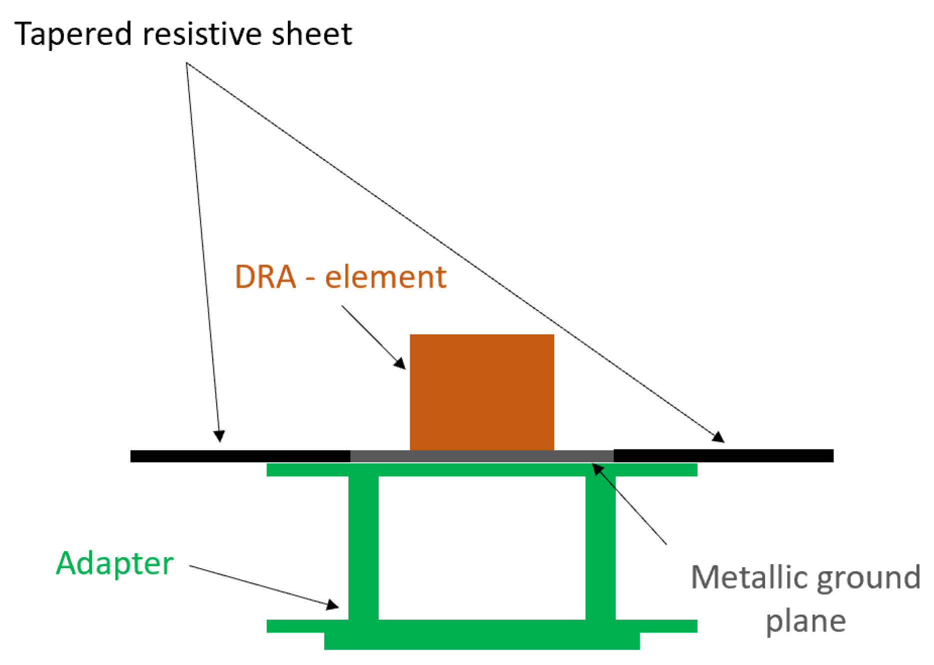
In addition to the resistivity gradient and selection of suitable gradient values, the positioning of the resistive sheet also plays a crucial role in determining the performance of the selected approach. As demonstrated in [8], entirely replacing the metallic ground plane with a material that maps the desired resistivity gradient can be an effective way to achieve improved performance. An alternative approach to attach a tapered resistive sheet that extends the metallic ground plane is shown in Figure 1. This approach, chosen for this paper, offers a more flexible and adaptable solution that can be tailored to meet the specific needs of the antenna design.

2.2. Antenna with Different Mounting Setups

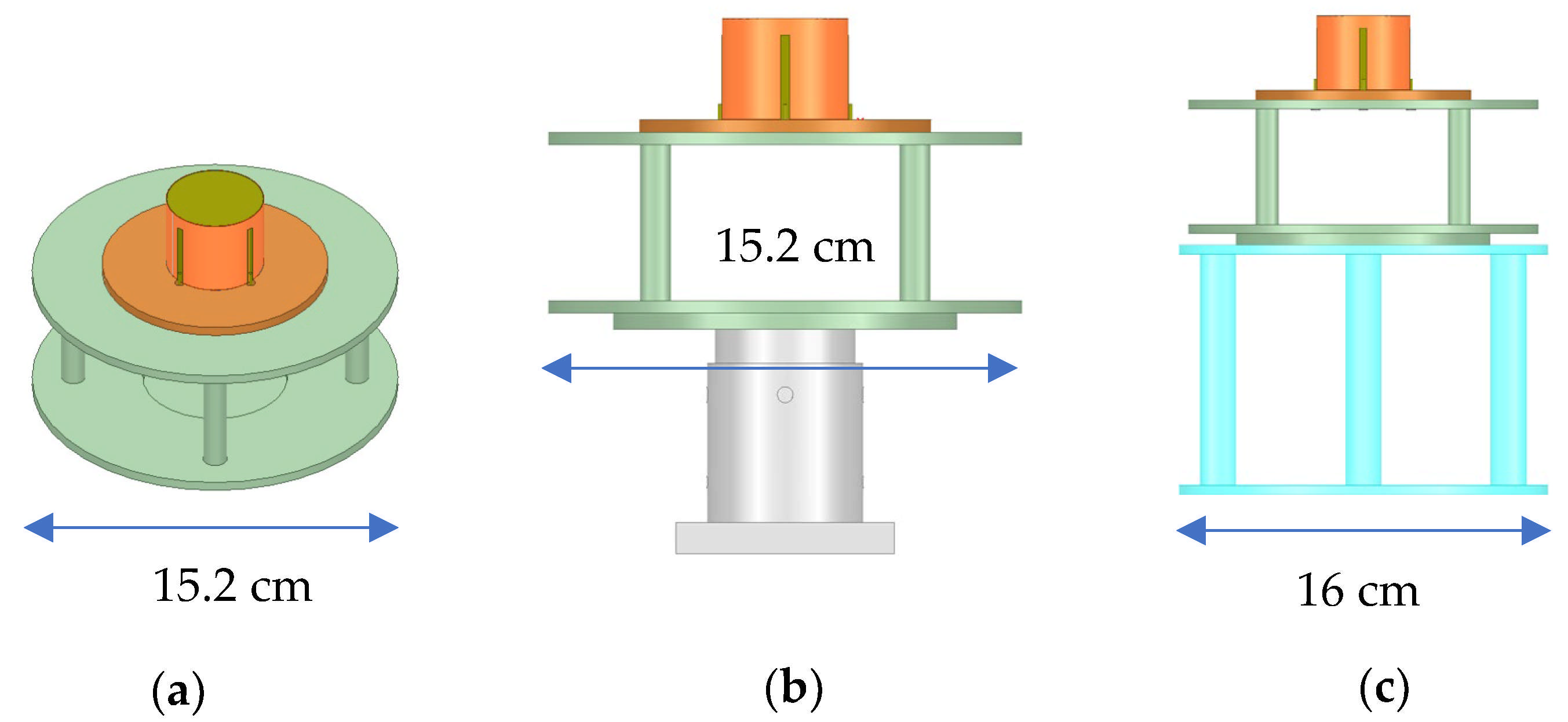
Here, we have used, as an example, an in-house built antenna with a dielectric resonator antenna (DRA) element. The antenna operates in a full GNSS L band from 1.1 to 1.6 GHz [10]. To investigate the mounting effects, two representative mounting models are placed concentrically below the antenna. The simulation setup comprises three distinct configurations, as depicted in Figure 2. Specifically, Figure 2a shows the antenna without any additional mounting, Figure 2b illustrates the antenna with a metallic mount, and Figure 2c depicts the antenna with a plastic mount. The adapter, depicted in green, is fabricated from 3D printed material, UltiMaker PLA (polylactic acid). The maximum diameter of the adapter is 15.2 cm, and the plastic mount is 16 cm. These setups are designed to simulate various real-world scenarios and to evaluate the performance of the modified antenna in different environments.

2.3. Modeling of Ideal Resistive Sheet

Our objective is to identify the most effective resistive sheet configuration. To achieve this, we consider an exponential gradient, as already described in [11], as basic geometry in our analysis. In general, the optimization of the resistive sheet is typically performed using an ideally tapered resistive sheet, which is considered to be infinitely thin and perfectly matches the resistivity gradient. This resistivity gradient is described by Equation (1) [13]:
Z x = e l n ( z f z 0 + 1 ) . x x m i n x m a x x m i n + z 0 1 .
The gradient exhibits an exponential behavior, with the surface resistivity Z varying as a function of the distance x from the ground plane center. The sheet spans a region between the inner boundary x m i n and the outer boundary x m a x , with resistivity values z 0 at x m i n and z f at x m a x . To identify the ideal starting and final resistivities, we established a cost function that serves as a guiding metric for the optimization process. This cost function is designed to minimize the variations in the antenna pattern when mounted on different holders, thereby ensuring that the optimal solution is achieved. The ideal resistive sheet is then optimized in Ansys HFSS using the cost function described in the next subsection.

2.4. Cost Function

To obtain a comprehensive and single-value description of the antenna’s performance, a cost function is defined that combines multiple antenna metrics, such as realized gain amplitude and phase. This function incorporates both the calculated metrics for the antenna with a metal mount and no mount, as well as the metrics for the antenna with a plastic mount and no mount. The optimization of the cost function is presented as
C O S T = f m t w 1 , f , m , t . x ¯ f , m , t + w 2 , f , m , t . σ f , m , t
where the different parameters are extended by specific weights w ( p , f , m , t ) , here p is 1 for mean and 2 for standard deviation. The cost function sums the absolute values of the mean ( x ¯ ) and standard deviation ( σ ) for each of the two mounting types ( m ), frequencies ( f ), and analyzed parameter ( t ), considering both gain amplitude and phase. The weights are used to assign varying levels of importance to each factor: frequency, mounting type, and analyzed parameter type, allowing for a more nuanced and accurate evaluation of the antenna’s performance. The definition of the weights is calculated by a combination of multiple factors defined above.
The metal mount factor is given more weight than the plastic mount in the analysis, as it is known to have a greater impact on the antenna’s radiation pattern. Additionally, the factor of the standard deviation is selected as more relevant in the calculation, as it provides a better description of the variation in the antenna’s performance. The final definition of the factors is presented in Table 1.
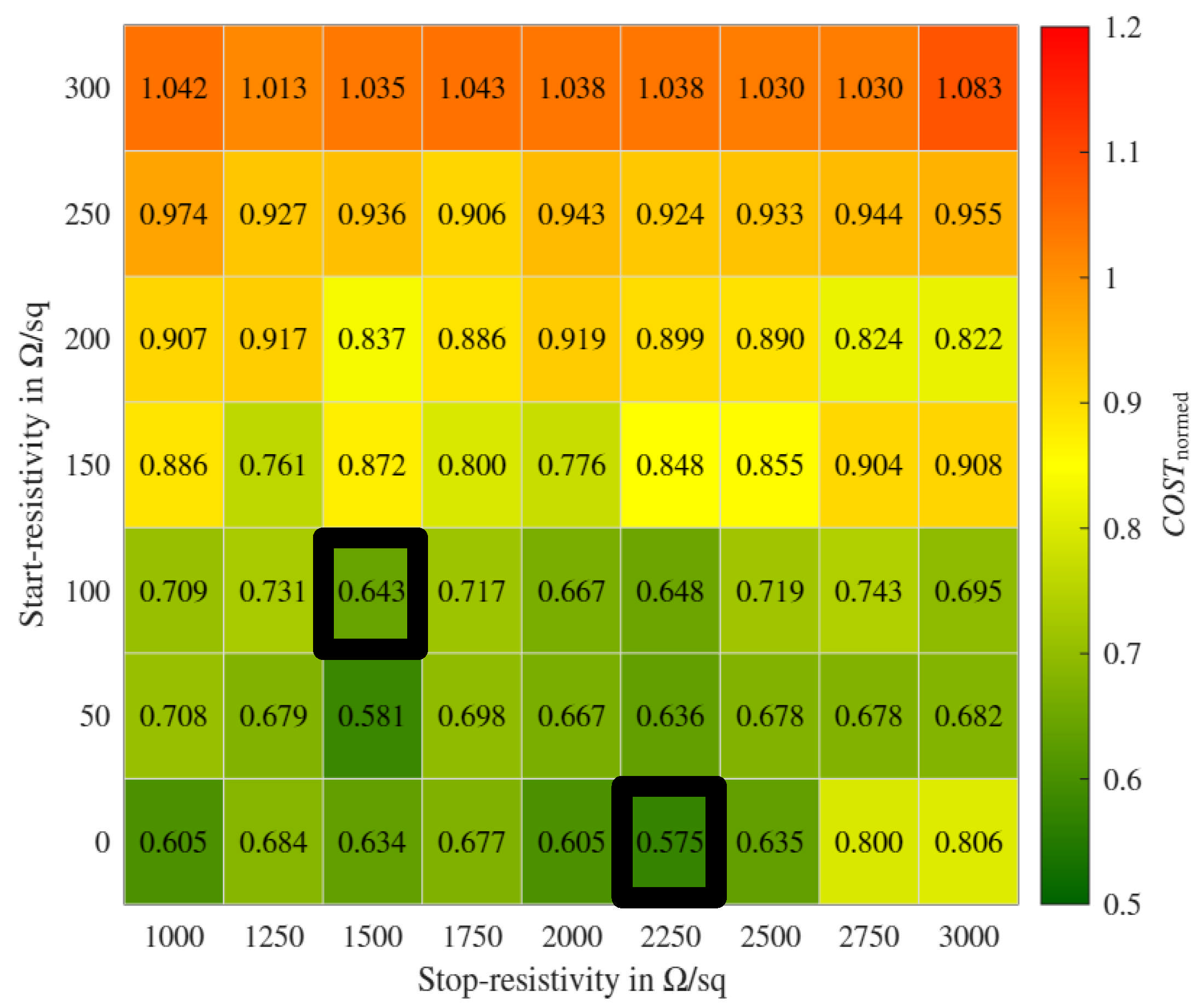
The simulation parameters for the resistive sheet have been tuned inside the practicable regions, specifically setting x m i n to the interior of the antenna and fixing x m a x at a value of 25 cm. The variables that were subject to optimization during the process were z 0 and z f . Figure 3 illustrates the resulting normalized cost values ( C O S T n o r m e d = C O S T C O S T i n i t i a l ) for the modified antenna design incorporating the resistive sheet, providing a visual representation of the optimization outcome. The green color indicates lower cost, while the red color represents higher cost. The best obtained cost values are circled in black and will be used later in the study.

3. Structure Manufacturing

According to the research presented in [14], it has been demonstrated that materials with suitable permittivity ( ε ) can be used to achieve a specific equivalent surface resistivity, given as
R e = j Z o k 0 τ ε ε 0 1 ,
with material thickness τ λ 0 and a relative permeability µ r = 1 . This finding has significant implications for the implementation of resistive sheets, as it suggests that such sheets can be theoretically realized by carefully selecting the permittivity of the material. This is, for instance, possible by the AM technique [15].
By employing spatially varying infill configurations, the structure was designed to exhibit gradient electromagnetic properties. The effective medium parameters were evaluated using a unit cell model under normal incidence excitation, enabling the characterization of the different unit cells’ electromagnetic behavior. The EM fields interact with the unit cell, leading to specific S-parameters, according to reflection and transmission properties. These parameters enable the calculation of the effective refraction index n e f f and effective wave impedance in the material z e f f , as defined in [16], which would lead to the calculation of effective material parameters of the designed unit cells.
For the manufacturing process, the FILAMAG-F filament is selected, provided by the manufacturer HYMAG’IN [17]. This filament is a polymer filled with magnetic nanoferrite powder, and according to the manufacturer’s information, it is capable of being manufactured as electromagnetic (EM) absorbing structures using a commercial Fused Deposition Modeling (FDM) 3D printer. The material is dispersive in nature, with relative permittivity ε r = 18.48 + 3.66 j at L5 center frequency and ε r = 17.63 + 3.15 j at L1 center frequency.
Due to the limitations of the additive manufacturing technology, such as minimum extrusion width, minimum and maximum layer heights and corresponding tolerances, the 3D periodic structure is not suitable to manufacture the range of permittivity values required to obtain the optimal resistivity range obtained in the previous section. To address this issue, a 2D periodic structure is considered, which can be manufactured with a single material layer. By decreasing the material thickness, the resistivity of the sheet can be increased, allowing for more effective absorption of electromagnetic waves and improved antenna performance.
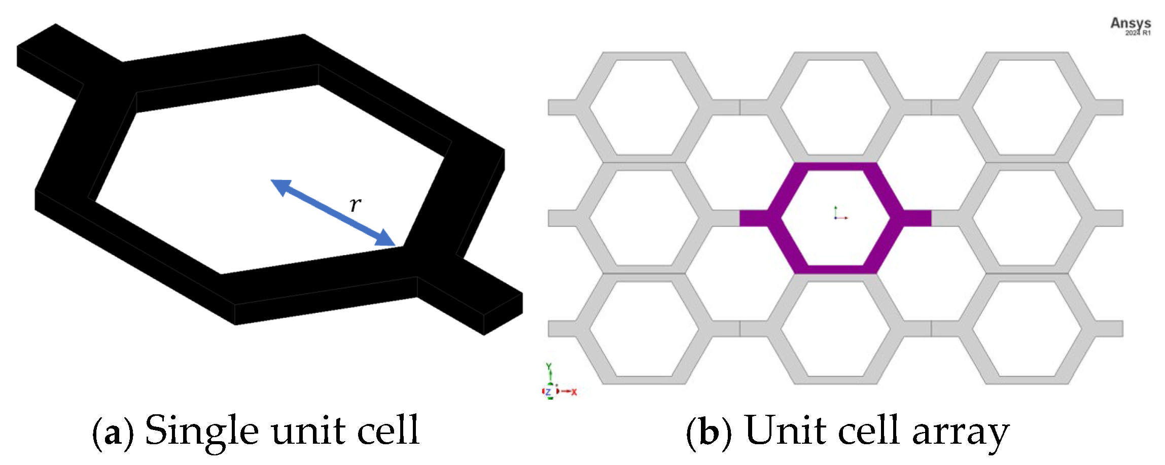
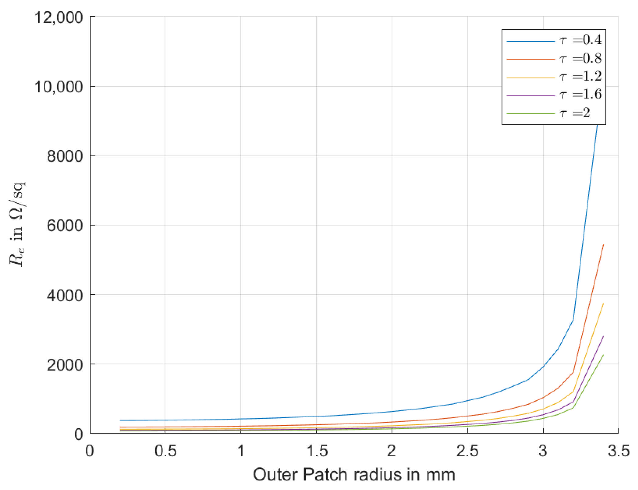
The structure design is performed with a MATLAB 2022b script. The 2D periodic structure consists of multiple hexagonal unit cells of size 7 mm, and its detailed configuration is clearly illustrated in Figure 4. By varying the outer patch radius r and material thickness τ , we can vary effective material properties. The equivalent resistivity of the realizable effective material parameters is then calculated using (3). Figure 5 presents a graphical representation of the equivalent resistivity values, illustrating how they change across r , with different line colors, visualizing material height.
The fabrication of this structure through additive manufacturing poses specific limitations due to the effect of the print process on the bulk material properties [18] and the minimum required size of the used nozzle (0.8 mm, as per manufacturer recommendations), limiting the minimal wall thickness to 0.8 mm. Due to the unit cell size of 7 mm, the maximum outer patch radius is then upper limited to 3.0 mm, hence resulting in a maximum achievable resistivity of 2000   / , while the minimum achievable resistivity is approximately 75 / (see Figure 5). Consequently, the theoretically optimal parameter set z 0 = 0   / and z f = 2250   / , as shown in Figure 3, is not realizable. On the other hand, it is possible to use the second optimal resistivity set, with z 0 = 100   / and z f = 1500   / .
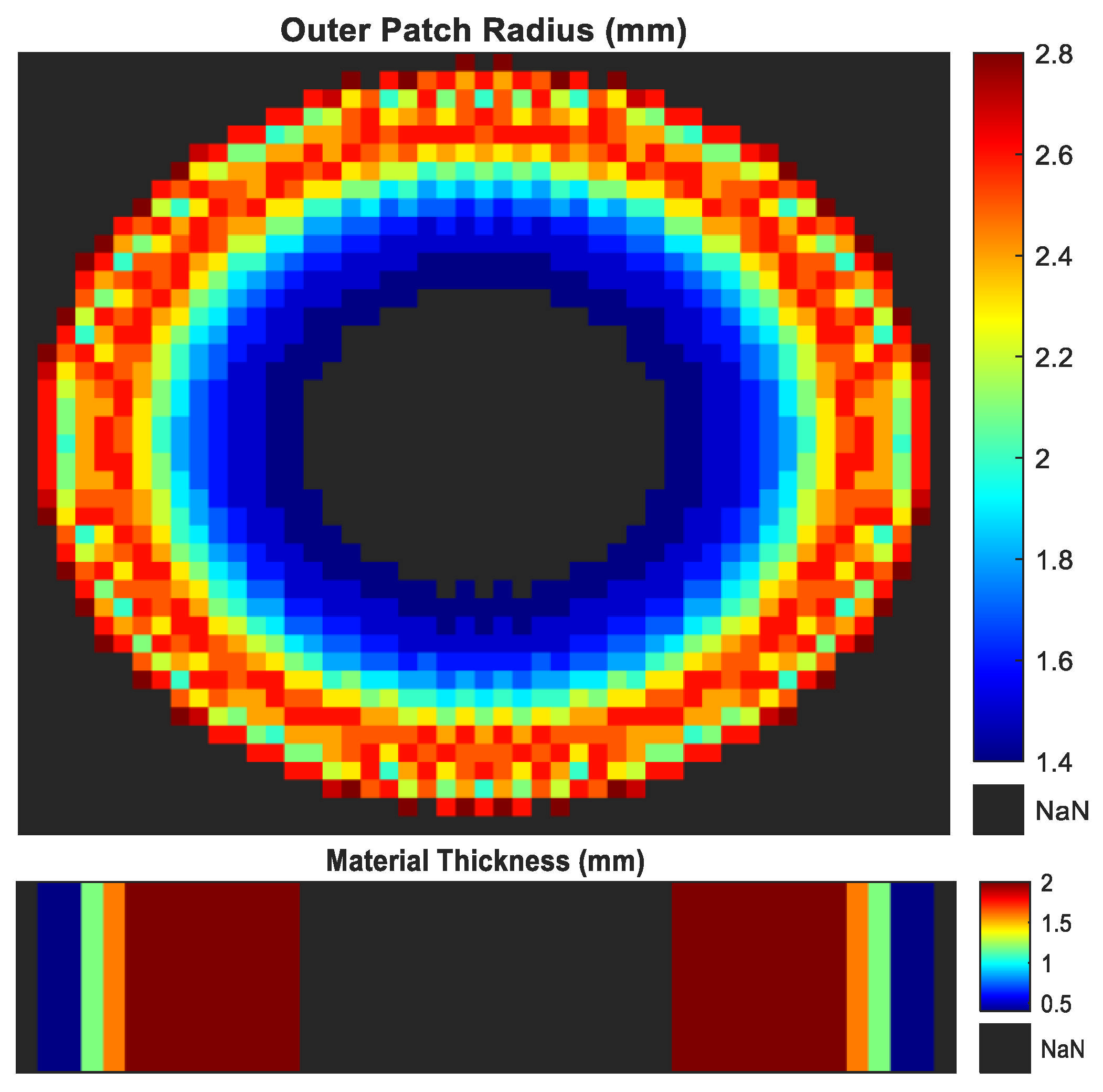
The optimized ideal resistivity values are then transformed into a required unit cell with specific material properties (e.g., permittivity), as defined by (3), which ultimately enables the creation of a complete 3D structure with a progressive resistivity profile that increases towards the outer regions. This is a significant departure from the ideal sheet concept presented in Section 2.2 where a simplified 2D representation was used. The final optimized values of outer patch radius and material thickness for the creation of each hexagonal unit cell are presented in Figure 6.
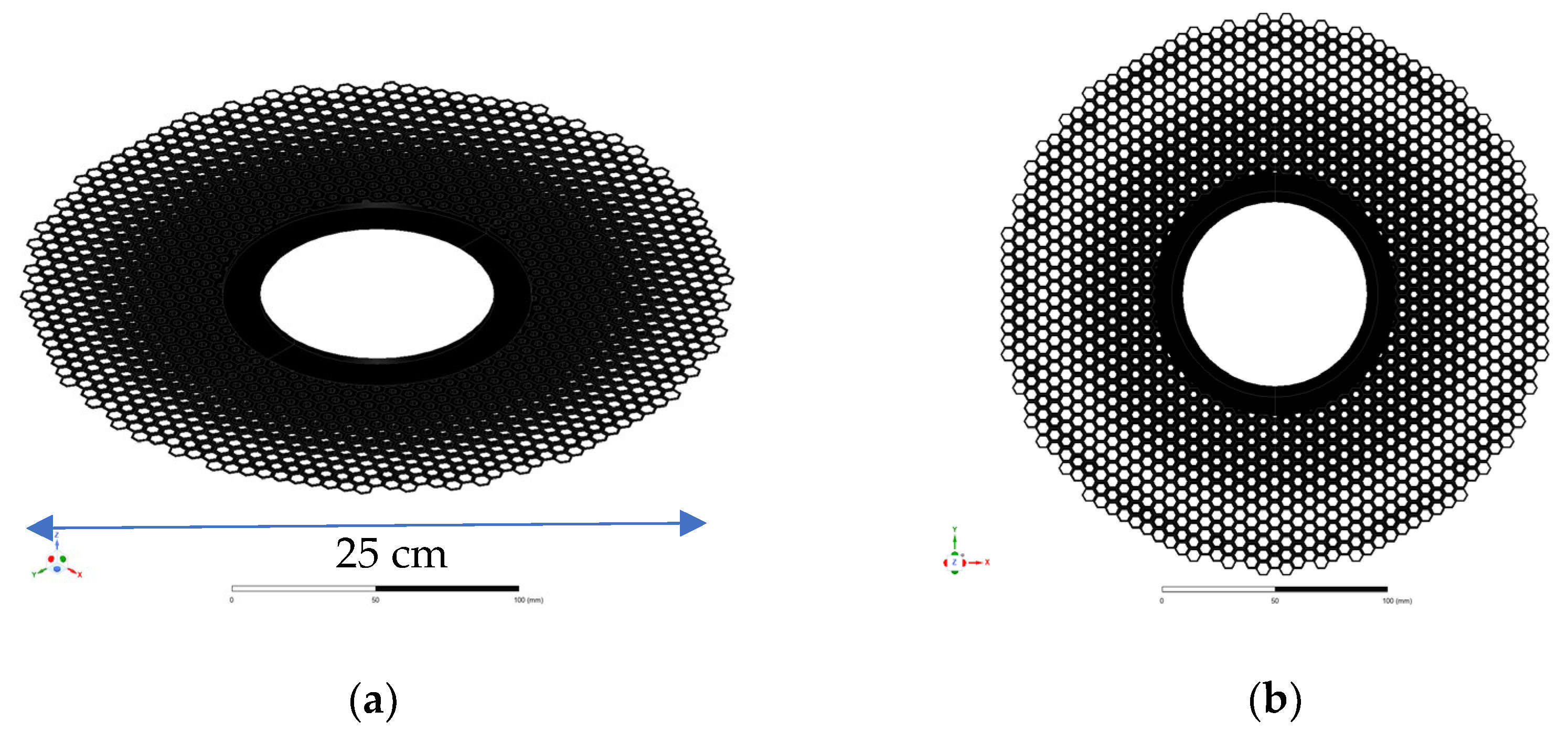
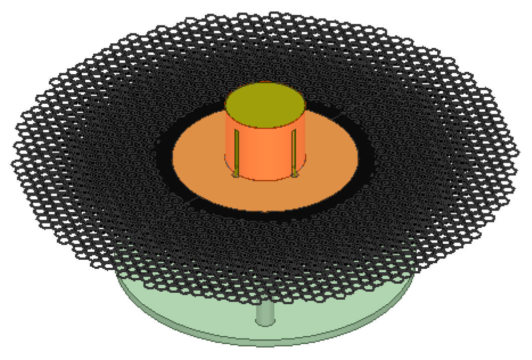
The resulting manufactured 3D structure is a complex electromagnetic entity that can be integrated into the antenna as an extended ground plane, as shown in Figure 7. To ensure mechanical uniformity and facilitate secure attachment, an additional layer of material is incorporated at the center of the structure (see Figure 7b).

4. Structure Analysis

4.1. Analysis with Different Setups: Simulation

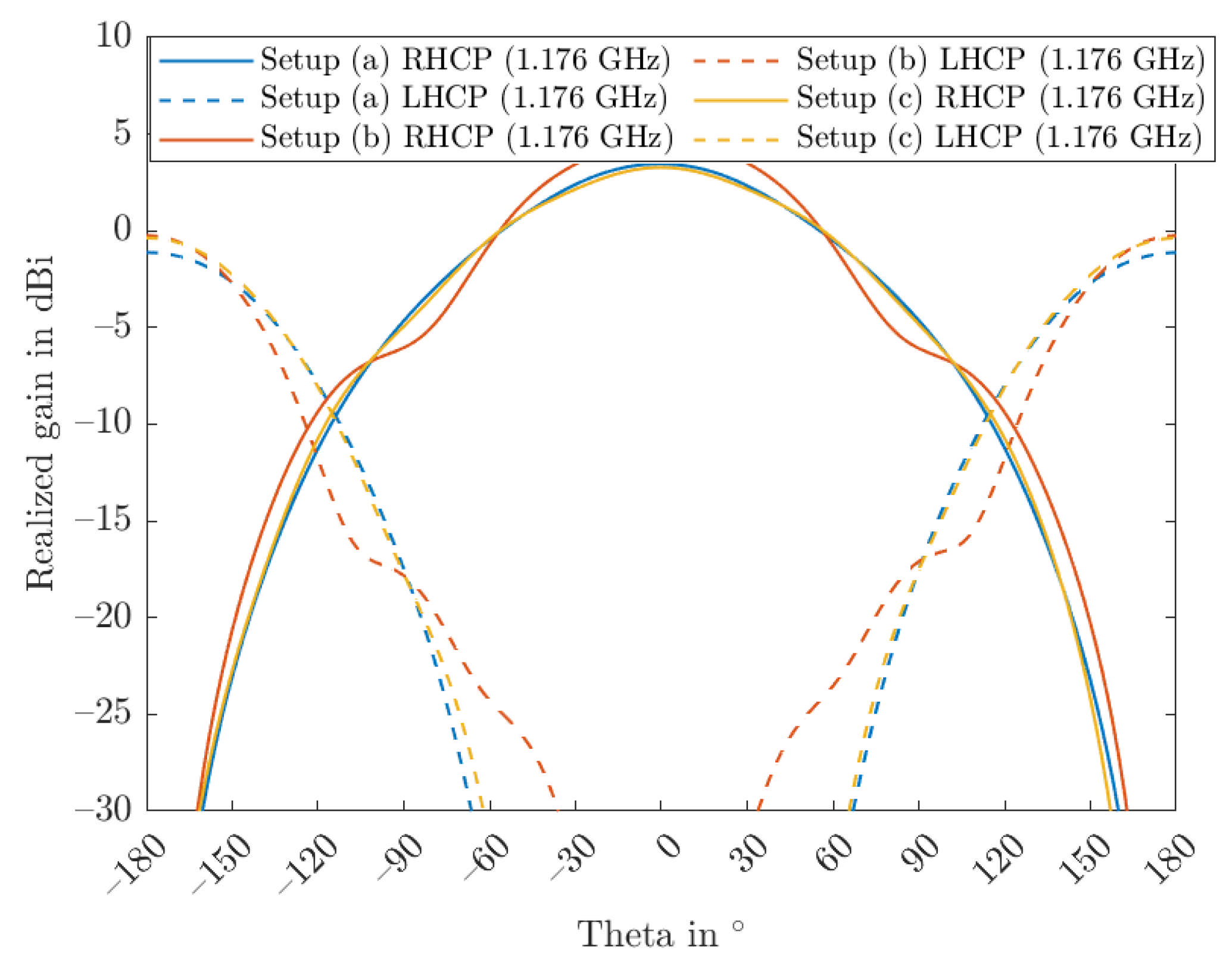
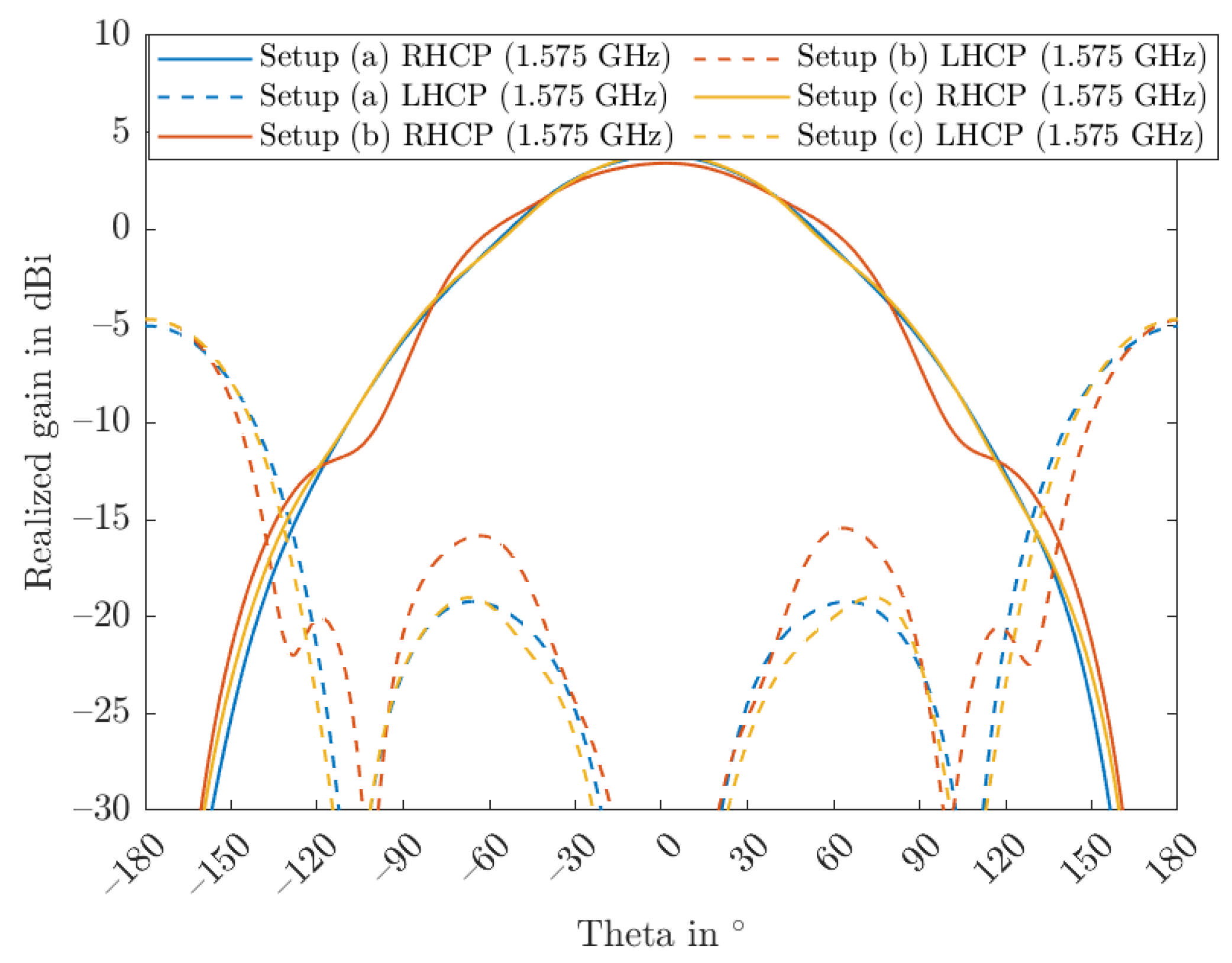
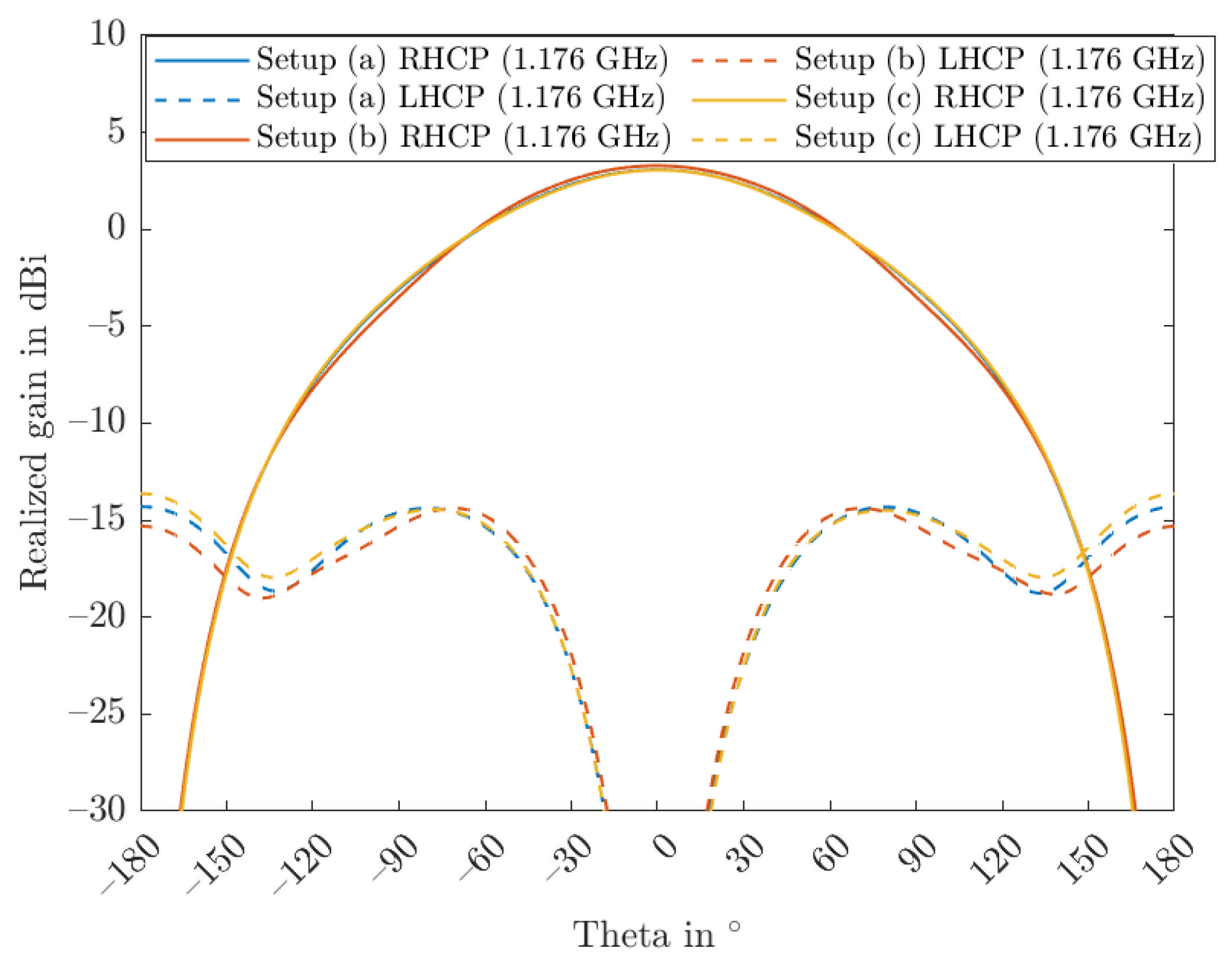
Next, the results of the antenna with and without structure are analyzed. Simulated realized gain for all setups with the initial antenna, as mentioned in Section 2.2, is shown in Figure 8 and Figure 9, for L5 and L1 center frequency, respectively. The initial antenna setup (a), as described, for E5a/L5 band, exhibits a realized RHCP gain of ~3.3 dBiC in the zenith direction, accompanied by a gain roll-off of ~8 dB. Also, for the E1/L1 band, the antenna achieves a realized RHCP gain of ~4 dBiC in the zenith direction, with a gain roll-off of ~10 dB.
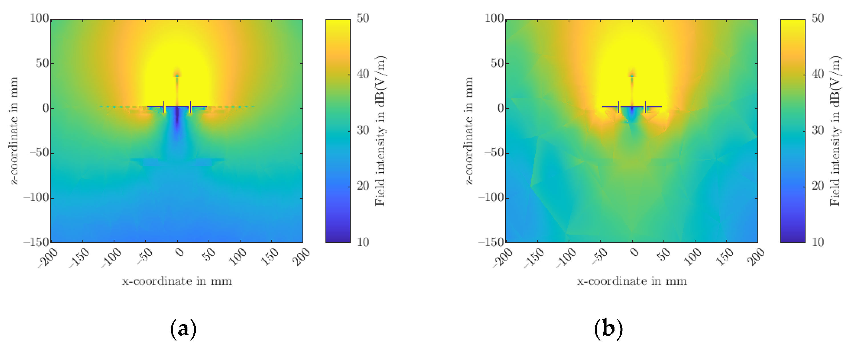
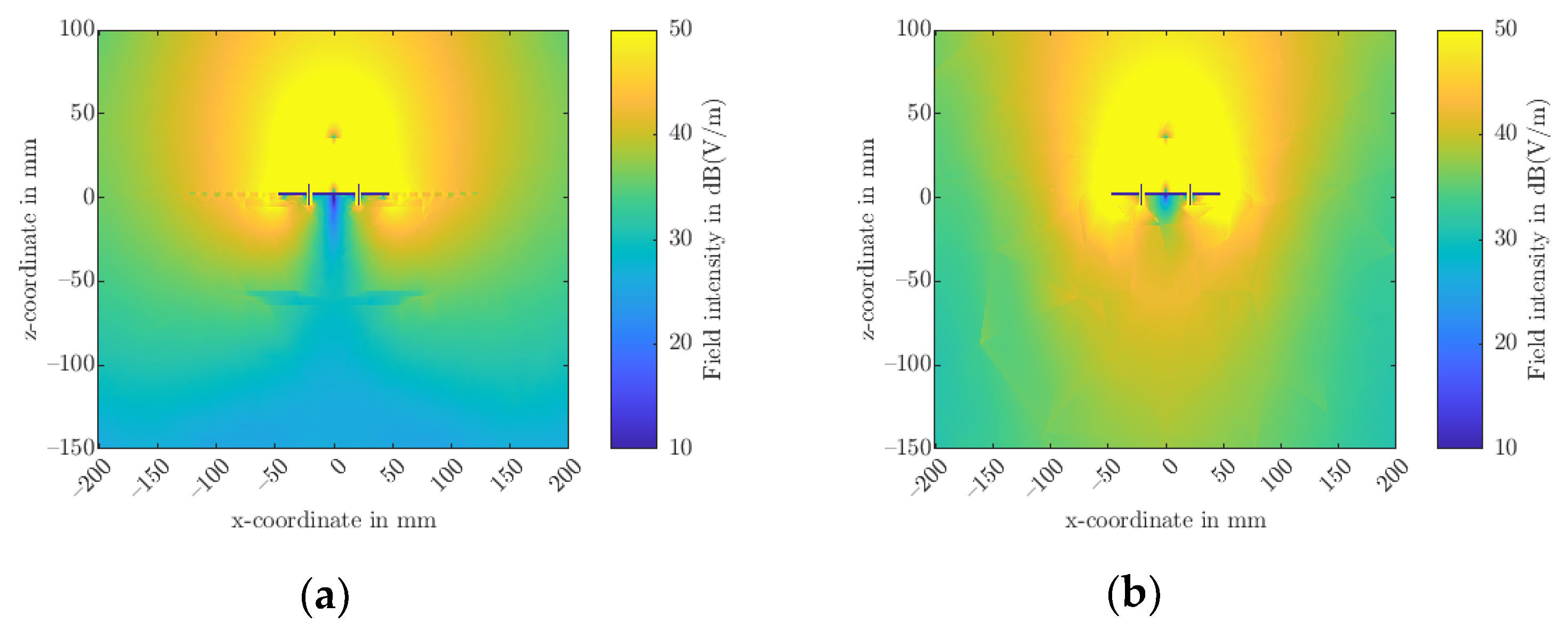
The modified antenna, which incorporates the addition of the optimized near-field (NF) structure, is depicted in Figure 10. The diameter of the antenna setup has been increased from 16 cm to 25 cm; however, this expansion was achieved without a significant increase in overall weight due to the use of 3D printed material. This modified antenna is a result of the design and optimization process discussed in the previous section. Figure 11 and Figure 12 show the near-field distributions of the initial and modified antennas at the L5 and L1 center frequencies, respectively. It is clearly evident that, after the integration of the proposed structure, the electromagnetic field intensity at the bottom of the antenna is significantly reduced compared to the initial design. This suppression of near-field energy minimizes the interaction between the antenna and nearby mounting structures, thereby reducing sensitivity to the surrounding environment and enhancing robustness in real-world installations.
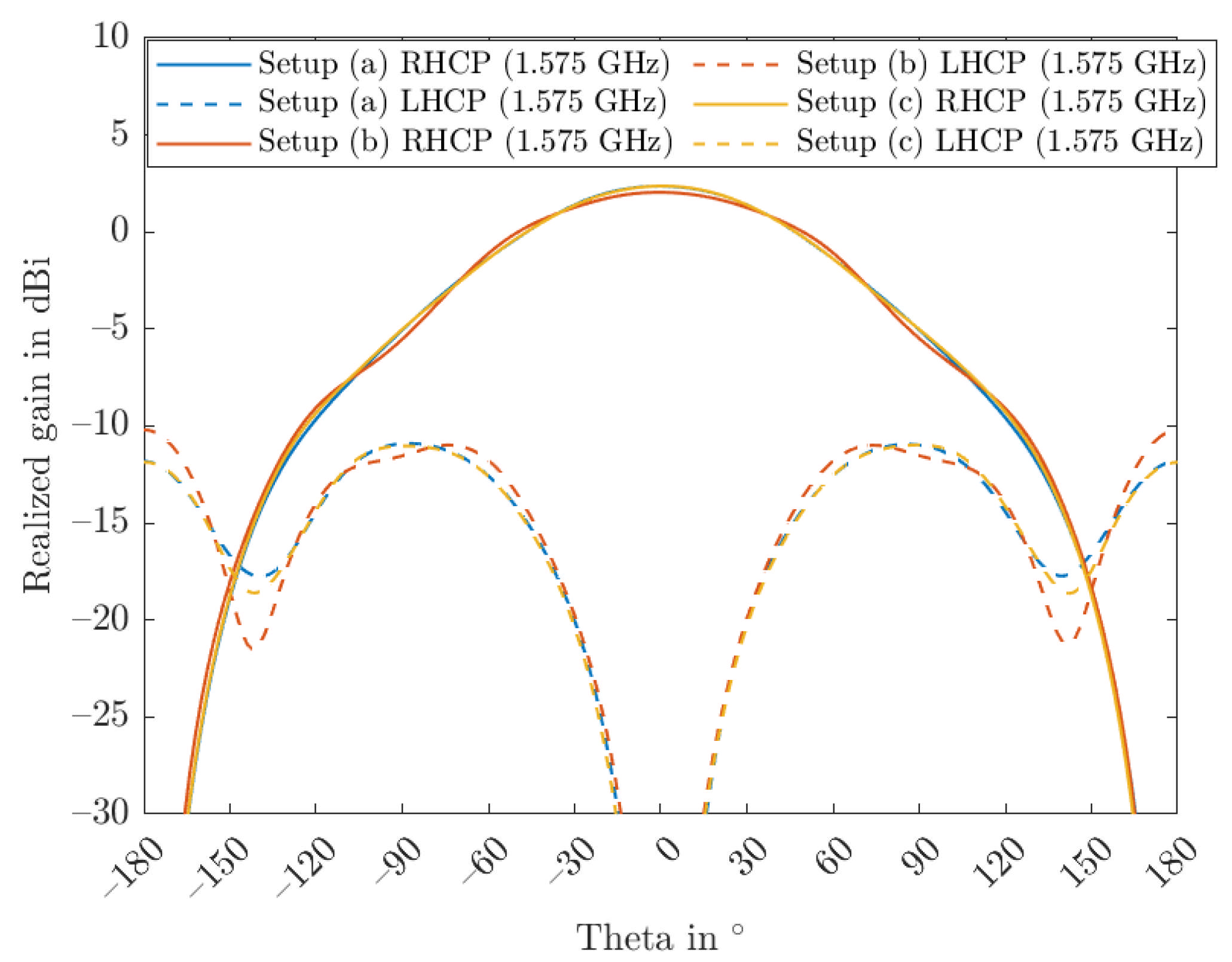
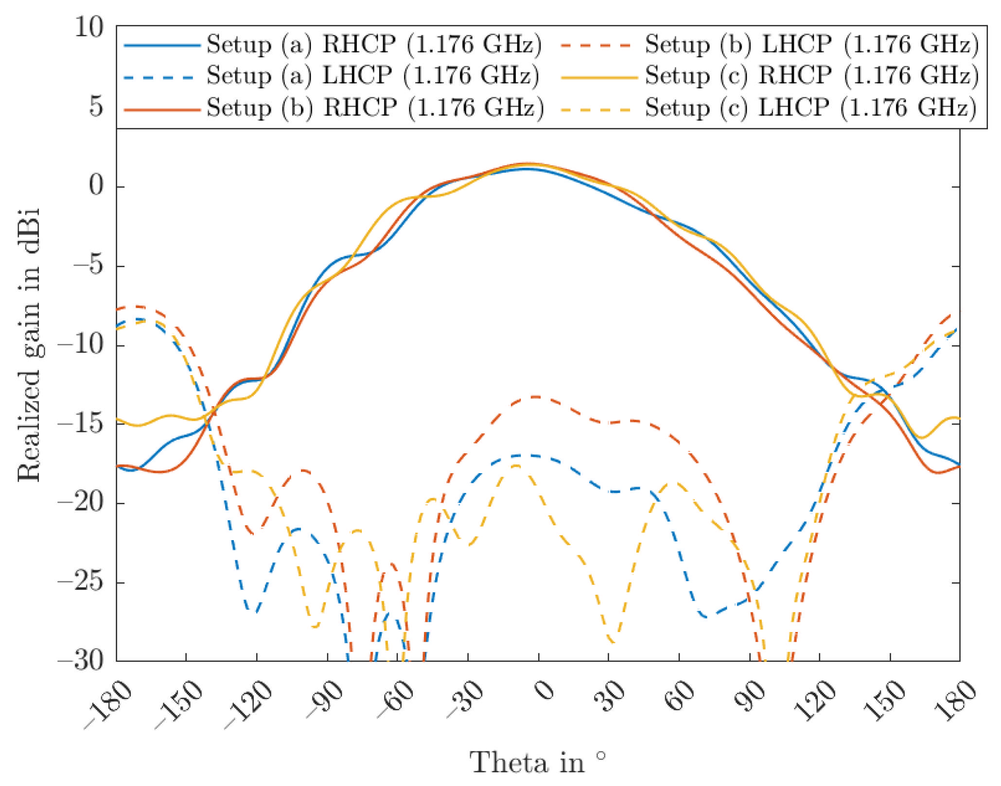
Similar to the initial antenna, the modified antenna is also tested using the three different setups mentioned in Figure 2. Simulated realized gain for all three setups is shown in Figure 13 and Figure 14, for L5 and L1 center frequency, respectively. Figures show that variations between the setups have reduced to a large extent. Additionally, the figures show a notable reduction in backlobes, which is a key factor in minimizing GNSS multipath effects.
The simulated initial antenna design had a cost function of 126, which served as a baseline for evaluating the performance of the antenna. However, through the modification of the antenna design with the inclusion of a near-field absorbing structure, the cost function of the new antenna design has been significantly reduced to 41. This represents an improvement of ~68% compared to the initial antenna design in simulation.

4.2. Analysis with Different Setups: Measurement

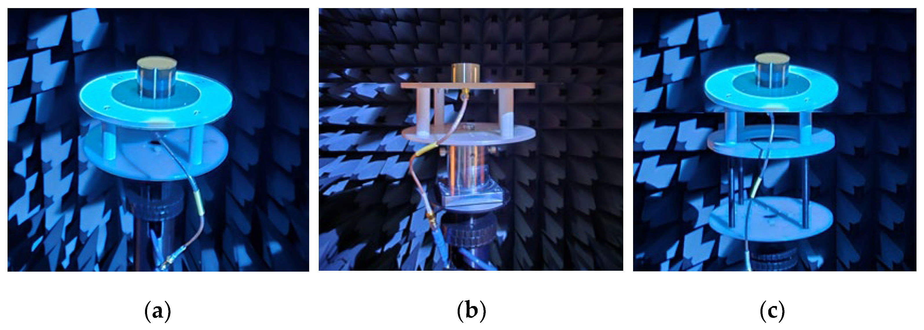
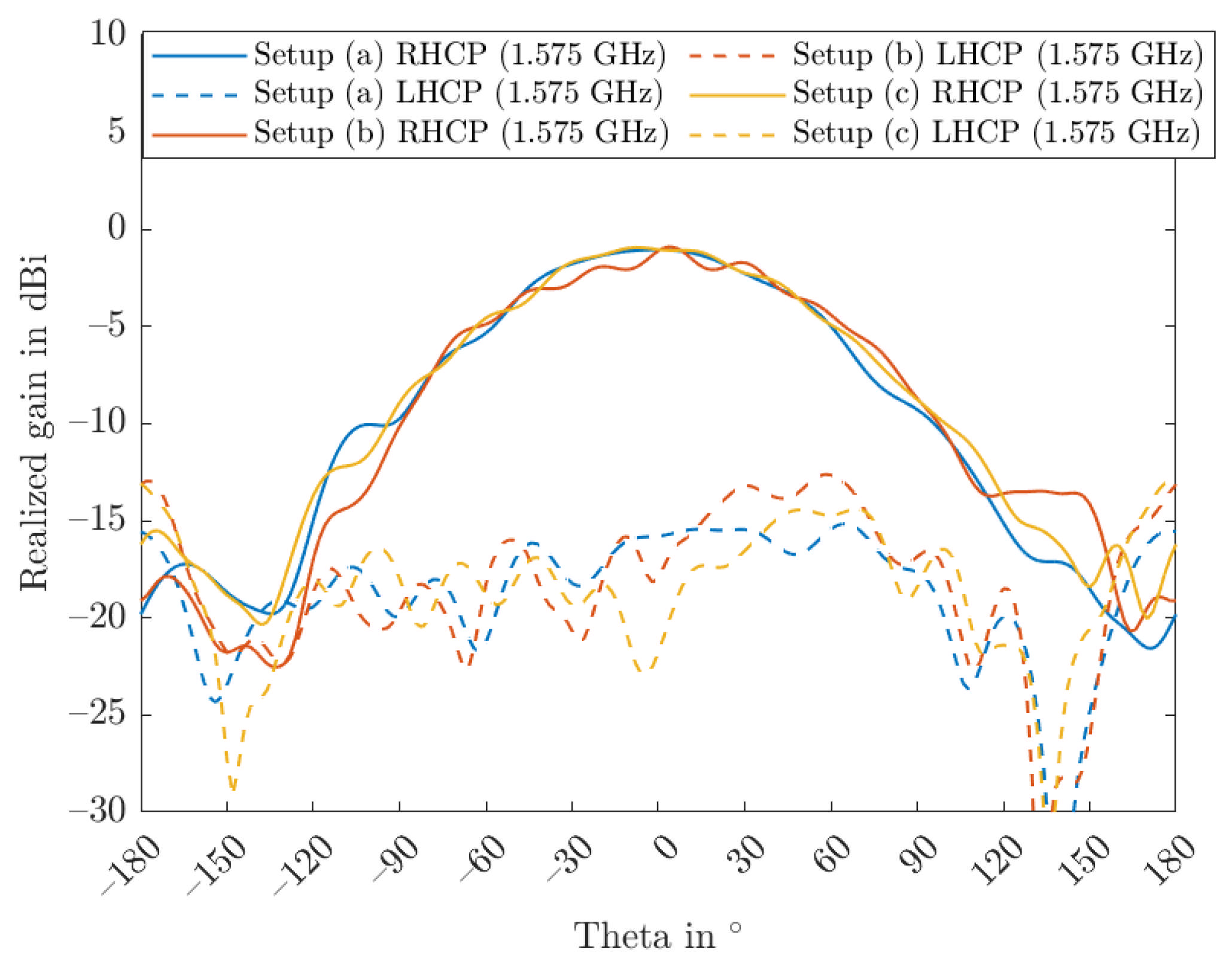
The next step in the evaluation of the antenna’s performance is to conduct measurements in our in-house available MVG’s near-field semi-anechoic chamber, known as Starlab. The initial antenna is measured in the Starlab chamber with all three defined setups that were previously discussed in Section 2.2. Exemplary pictures of different setups during measurements are shown in Figure 15, with no mount, a metal mount and a plastic mount. Measured 2D realized gain patterns are shown in Figure 16 and Figure 17, for L5 and L1 center frequency, respectively.
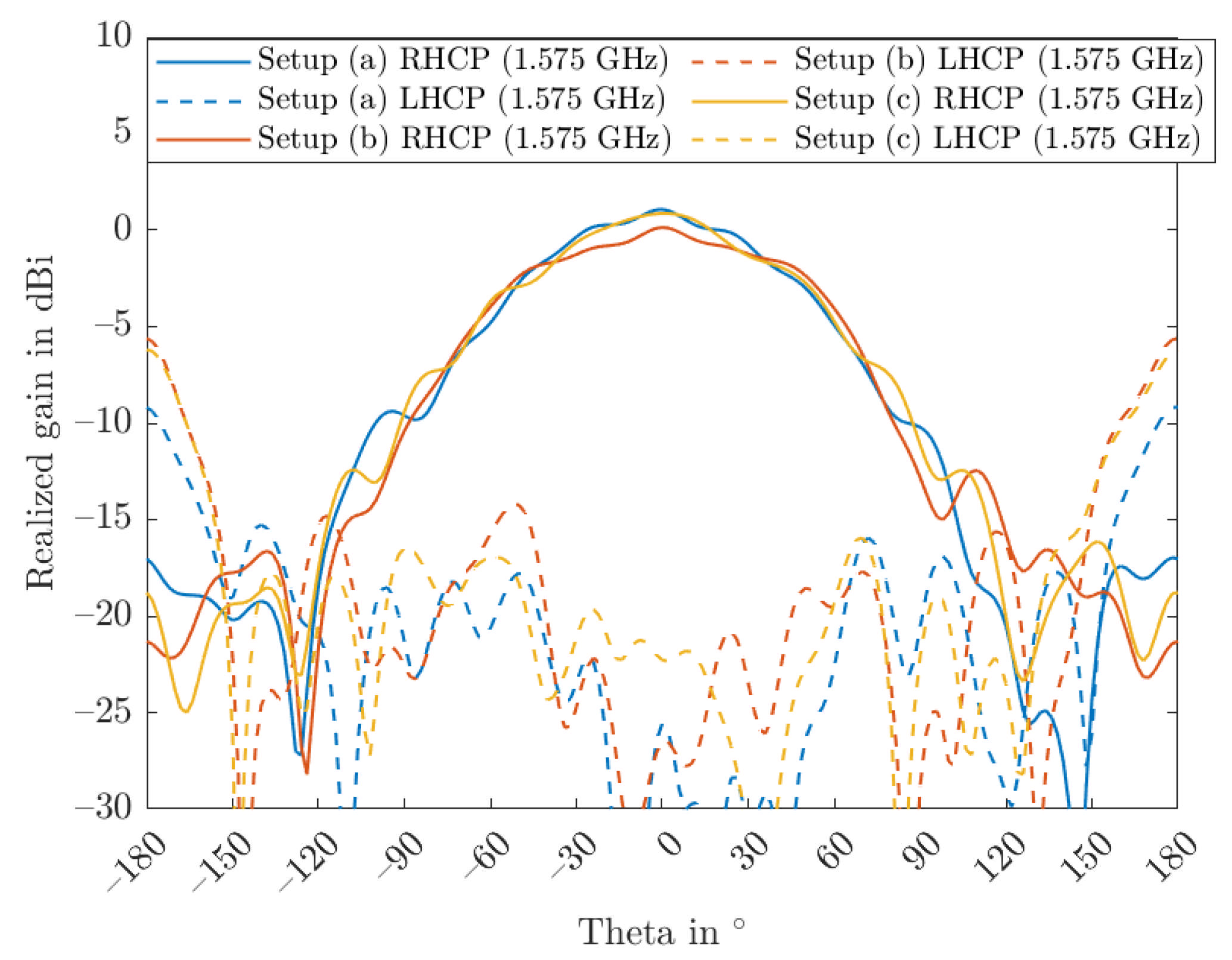
The initial prototype antenna design exhibited a measured cost function of 268, which was significantly higher than the simulated value of 126. Also, more oscillations and differences are clearly visible in the radiation pattern plots. Several factors may have contributed to this discrepancy, including imperfections in the manufacturing process, feed lines, and the inclusion of a PCB with microstrip lines. Since this work focuses on the design of the absorbing structure and not of the antenna per se, this is, however, not a limiting factor.
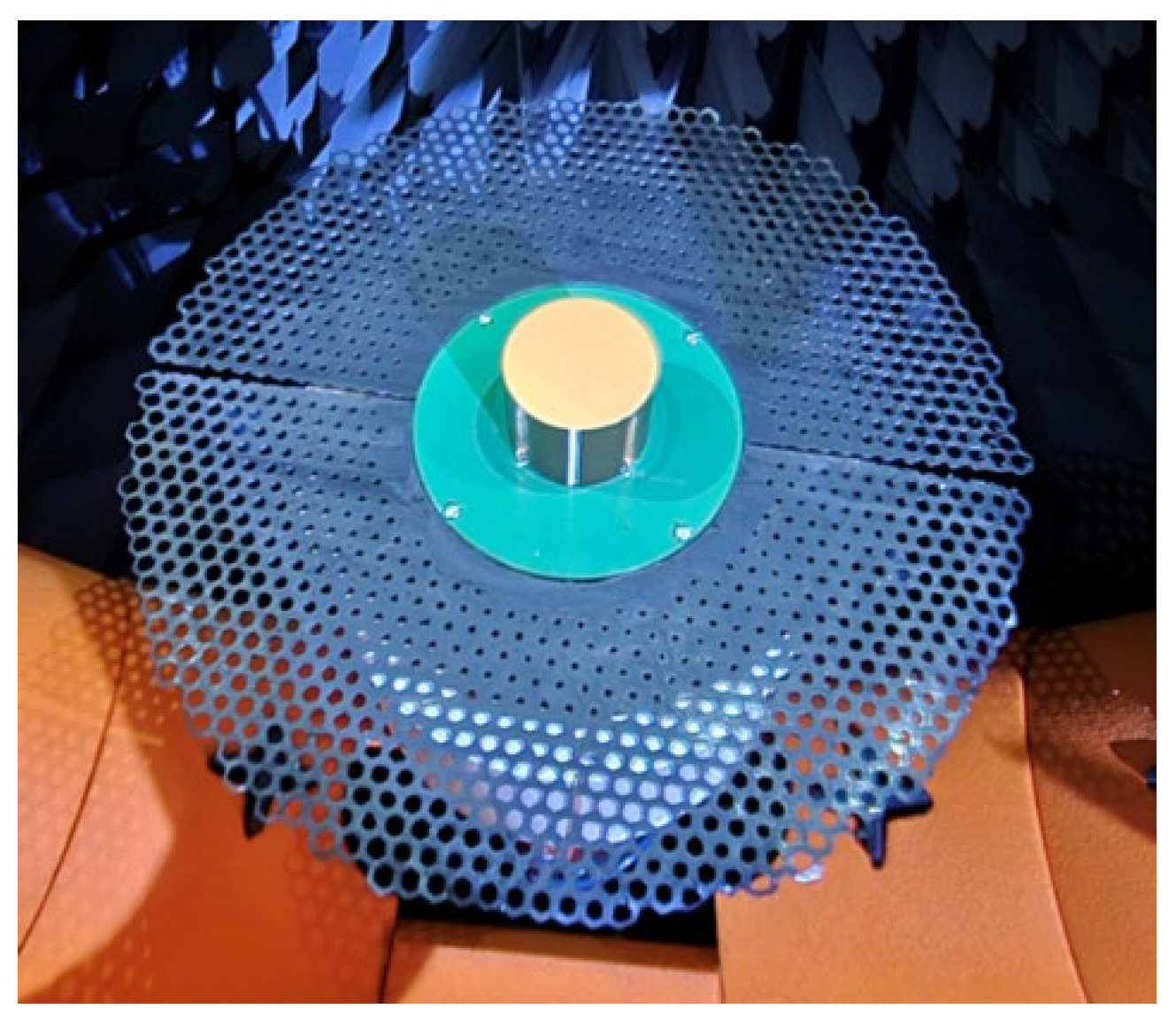
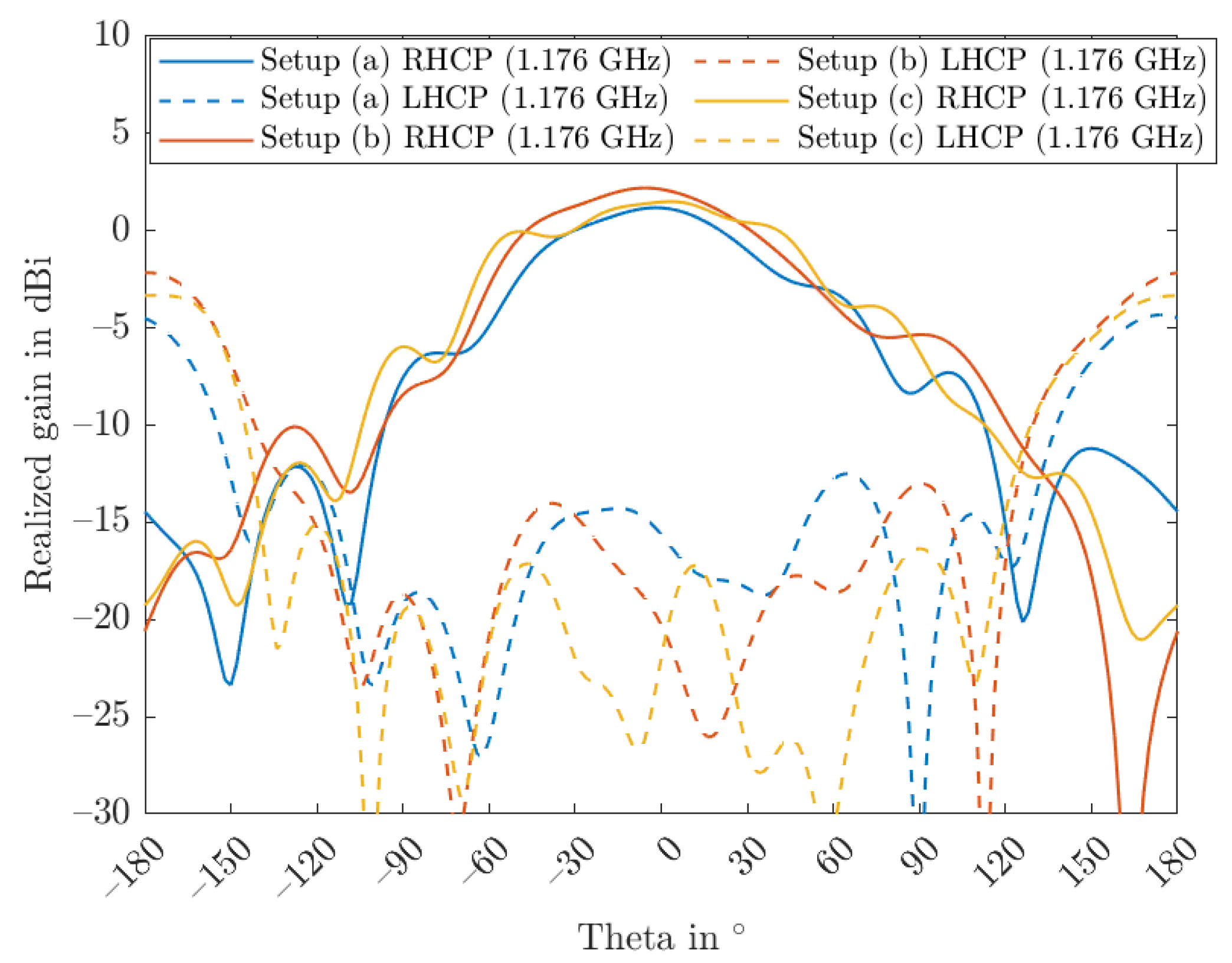
Next, the modified antenna is measured in the Starlab chamber, as shown in Figure 18. Obtained 2D realized gain patterns are provided in Figure 19 and Figure 20, for L5 and L1 center frequency, respectively.
The integration of the absorbing structure with a tapered resistivity profile has led to a significant improvement in the antenna’s performance, reducing the cost function to 123, which is a reduction of approximately 54% to its initial value. Concurrently, the maximum backlobe level has been suppressed by more than 5 dB compared to the original design, demonstrating enhanced radiation pattern control and reduced sensitivity to near-field disturbances.


5. Conclusions

In this paper, a novel structure was developed to minimize the dependence on mounting structures by leveraging the concept of tapered resistive sheets. The designed structure was realized using AM techniques, which enabled the creation of complex geometries and control over the sheet’s effective properties. The measurement results demonstrated that among the various mounting setups considered, the modified antenna with the NF structure achieved a very good cost value improvement, with a remarkable 54% reduction in cost value. This achievement leads to a reduced impact of mountings on the antenna’s performance in terms of gain amplitude and phase, as well as a decrease in backlobe radiation, which in turn contributes to an improvement in GNSS multipath performance.
Author Contributions

Conceptualization, V.T. and S.C.; methodology, V.T., C.I. and S.C.; software, C.I.; validation, V.T., C.I. and S.C.; formal analysis, C.I.; investigation, C.I., S.H. and W.E.; data curation, V.T. and C.I.; writing—original draft preparation, V.T., C.I., S.H. and S.C. All authors have read and agreed to the published version of the manuscript.

Funding

This research received no external funding.

Data Availability Statement

The original contributions presented in this study are included in the article. Further inquiries can be directed to the corresponding author.

Conflicts of Interest

The authors declare no conflicts of interest.

References

  1. Wanninger, L. Correction of apparent position shifts caused by GNSS antenna changes. GPS Solut. 2009, 13, 133–139. [Google Scholar] [CrossRef]
  2. Wübbena, G.; Schmitz, M.; Menge, F.; Seeber, G.; Völksen, C. A new approach for field calibration of absolute antenna phase center variations. Navigation 1997, 44, 247–256. [Google Scholar] [CrossRef]
  3. Kersten, T.; Schön, S. GPS code phase variations (CPV) for GNSS receiver antennas and their effect on geodetic parameters and ambiguity resolution. J. Geod. 2017, 91, 579–596. [Google Scholar]
  4. Wübbena, G.; Schmitz, M.; Boettcher, G. Near-field effects on GNSS sites: Analysis using absolute robot calibrations and procedures to determine corrections. In Proceedings of the IGS Workshop; IGS: Pasadena, CA, USA, 2006; pp. 8–12. [Google Scholar]
  5. Dilssner, F.; Seeber, G.; Wübbena, G.; Schmitz, M. Impact of near-field effects on the GNSS position solution. In Proceedings of the 21st International Technical Meeting of the Satellite Division of the Institute of Navigation (ION GNSS 2008), Savannah, GA, USA, 16–19 September 2008; pp. 612–624. [Google Scholar]
  6. Görens, B.; Kersten, T.; Schön, S.; Zimmermann, F.; Wanninger, L.; Becker, M.; Villinger, A.; Mayer, M.; Kuhlmann, H. Berücksichtigung von Antennenkorrekturen bei GNSS-Anwendungen, 2018. Available online: https://dvw.de/api/assets/downloads/ev/publikationen/merkblatter/01_dvw-merkblatt_antennenkorrekturen-gnss_2018_v3.pdf (accessed on 7 June 2026).
  7. Wang, S.; Li, K.; Kong, F.; Du, L. A miniaturized triple-band planar antenna combing single-cell metamaterial structure and defected ground plane for WLAN/WiMAX applications. J. Electromagn. Waves Appl. 2021, 35, 357–370. [Google Scholar] [CrossRef]
  8. Dong, J.; Hua, Q. Overview and Progress of GNSS Anti-multipath Antenna Designs. Sens. Mach. Learn. Appl. 2023, 2, 22. [Google Scholar] [CrossRef]
  9. Baggen, R.; Martínez-Vázquez, M.; Leiss, V.; Holzwarth, V.; Drioli, L.S.; de Maagt, P. Low profile GALILEO antenna using EBG technology. IEEE Trans. Antennas Propag. 2008, 56, 667–674. [Google Scholar] [CrossRef]
  10. Tripathi, V.; Elmarissi, W.; Caizzone, S. Advanced Choke Ring Antenna for Enhanced GNSS Reference Station Performance. In Proceedings of the Navitec 2026, Noordwijk, The Netherlands, 20–22 May 2026; Available online: https://elib.dlr.de/216774/ (accessed on 6 May 2026).
  11. Rao, B.R.; Williams, J.H.; Rosario, E.N.; Davis, R.J. Gps microstrip antenna array on a resistivity tapered ground plane for multipath mitigation. In Proceedings of the 13th International Technical meeting of the Satellite Division of The Institute of Navigation (ION GPS 2000), Salt Lake City, UT, USA, 19–22 September 2000; pp. 2468–2476. [Google Scholar]
  12. Du, L.; Fu, Y. A small wideband low-multipath GNSS antenna using resistive film. IEEE Antennas Wirel. Propag. Lett. 2013, 12, 1045–1048. [Google Scholar] [CrossRef]
  13. Handel, C.S. Low Frequency Modification of a Dual Chamber Compact Range. Master’s Thesis, The Ohio State University, Columbus, OH, USA, 1997. Available online: http://rave.ohiolink.edu/etdc/view?acc_num=osu1729783606608307 (accessed on 23 June 2025).
  14. Senior, T.B.A.; Volakis, J.L. Approximate Boundary Conditions in Electromagnetics; No. 41; IET: London, UK, 1995. [Google Scholar]
  15. Hehenberger, S.P.; Caizzone, S.; Yarovoy, A.G. Additive manufacturing of linear continuous permittivity profiles and their application to cylindrical dielectric resonator antennas. IEEE Open J. Antennas Propag. 2023, 4, 373–382. [Google Scholar] [CrossRef]
  16. Smith, D.R.; Vier, D.C.; Koschny, T.; Soukoulis, C.M. Electromagnetic parameter retrieval from inhomogeneous metamaterials. Phys. Rev. E 2005, 71, 036617. [Google Scholar] [CrossRef] [PubMed]
  17. HYMAG’IN. Filamag-F. Available online: https://www.hymagin.com/products/absorbing-filament/filamag-f/ (accessed on 1 June 2026).
  18. Wu, Y.; Isakov, D.; Grant, P.S. Fabrication of Composite Filaments with High Dielectric Permittivity for Fused Deposition 3D Printing. Materials 2017, 10, 1218. [Google Scholar] [CrossRef] [PubMed]
Figure 1. Illustration of resistive sheet extending ground plane.
Electronics 15 02651 g001
Figure 2. Setup of initial antenna, with mountings. (a) No mount. (b) Metal mount. (c) Plastic mount.
Electronics 15 02651 g002
Figure 3. Normalized cost values of the modified antenna (selected values in black square).
Electronics 15 02651 g003
Figure 4. Unit cell of 2D structure with outer patch radius 3 mm. (a) Single unit cell. (b) Unit cell array (with highlighted single unit cell).
Electronics 15 02651 g004
Figure 5. Selected equivalent resistivity curve for design process ( τ in mm).
Electronics 15 02651 g005
Figure 6. Optimized outer patch radius (mm) and material thickness (mm) for each unit cell in the structure.
Electronics 15 02651 g006
Figure 7. Model of implemented structure. (a) Side view. (b) Top view.
Electronics 15 02651 g007
Figure 8. Simulated radiation pattern of initial antenna with different setups for L5 center frequency.
Electronics 15 02651 g008
Figure 9. Simulated radiation pattern of initial antenna with different setups for L1 center frequency.
Electronics 15 02651 g009
Figure 10. Simulation setup of modified antenna.
Electronics 15 02651 g010
Figure 11. Near-field of the antenna at L5 center frequency. (a) Modified antenna. (b) Initial antenna.
Electronics 15 02651 g011
Figure 12. Near-field of the antenna at L1 center frequency. (a) Modified antenna. (b) Initial antenna.
Electronics 15 02651 g012
Figure 13. Simulated radiation pattern of modified antenna with different setups for L5 center frequency.
Electronics 15 02651 g013
Figure 14. Simulated radiation pattern of modified antenna with different setups for L1 center frequency.
Electronics 15 02651 g014
Figure 15. Measurement of initial antenna, with mountings. (a) No mount. (b) Metal mount. (c) Plastic mount.
Electronics 15 02651 g015
Figure 16. Measured radiation pattern of initial antenna with different setups for L5 center frequency.
Electronics 15 02651 g016
Figure 17. Measured radiation pattern of initial antenna with different setups for L1 center frequency.
Electronics 15 02651 g017
Figure 18. Measurement of modified antenna with no mount.
Electronics 15 02651 g018
Figure 19. Measured radiation pattern of modified antenna with different setups for L5 center frequency.
Electronics 15 02651 g019
Figure 20. Measured radiation pattern of modified antenna with different setups for L1 center frequency.
Electronics 15 02651 g020
Table 1. Cost function factors.
Phase factor 2.5
Gain factor1
Mean factor0.4
Standard deviation factor2
Frequency 1.176 GHz factor1
Frequency 1.575 GHz factor1.2
Metal mount factor2
Plastic mount factor0.8
Disclaimer/Publisher’s Note: The statements, opinions and data contained in all publications are solely those of the individual author(s) and contributor(s) and not of MDPI and/or the editor(s). MDPI and/or the editor(s) disclaim responsibility for any injury to people or property resulting from any ideas, methods, instructions or products referred to in the content.