Article

Design of a Sub-6 GHz CMOS Power Amplifier with a High-Q Glass Transformer for Off-Chip Output-Matching Networks

1
Department of Electronic Engineering, Soongsil University, Seoul 06978, Republic of Korea
2
ICT Device & Packaging Research Center, Korea Electronics Technology Institute, Seongnam-si 13509, Republic of Korea
3
Department of Intelligent Semiconductors, Soongsil University, Seoul 06978, Republic of Korea
*
Author to whom correspondence should be addressed.
Electronics 2025, 14(21), 4261; https://doi.org/10.3390/electronics14214261
Submission received: 8 October 2025 / Revised: 27 October 2025 / Accepted: 29 October 2025 / Published: 30 October 2025
(This article belongs to the Special Issue Advances in Analog and RF Circuit Design)

Abstract

This paper investigates and evaluates a compact, high-Q glass transformer with a 3D spiral structure that offers low loss and high area efficiency. Furthermore, we designed a CMOS power amplifier (PA) with an output-matching network implemented using an off-chip high-Q glass transformer to validate its operation. Two transformer types were developed: a five-port transformer with a center-tap and a four-port transformer without a center tap. The high-Q property of the transformer leads to low loss and tight coupling, as evidenced by an increase in maximum available gain (MAG). Compared with an integrated CMOS transformer, the high-Q transformer exhibits significantly lower loss while maintaining similar area and inductance, despite being an external component. A test PA comprising the CMOS PA and the off-chip transformer was evaluated with simulations and measurements, and it was also compared with a fully integrated PA at the simulation level to verify performance improvements. The proposed PA achieved a saturation power of 29.8 dBm, which was 1.7 dB higher than that of the fully integrated PA. The PAE also improved by 11 percentage points, from 32.1% to 43.1% in simulation. The results show substantial performance gains in simulation, while the total area increases only slightly. Measurements show the same trend as the simulations; with shorter bond-wire lengths, the measured results are expected to approach the simulated performance. These findings demonstrate the feasibility of an ultra-compact CMOS–off-chip hybrid PA that delivers high performance while maintaining a footprint comparable to that of a fully integrated PA, enabling applications in compact devices including mobile products.

1. Introduction

With advances in modern integrated circuit (IC) fabrication processes, ICs have been applied across a wide range of fields, spanning both commercial and military domains. Although process technology continues to improve, and printed circuit board (PCB)-based modules are increasingly consolidated into integrated implementations, planar layout constraints and process-driven passive losses still impose fundamental limits. To address these limitations, several approaches have been explored; among them, the hybrid circuit method—placing the IC on a PCB with discrete passive components—has been widely adopted, as discrete passives generally exhibit much higher Q (lower loss) than their on-chip counterparts [1,2,3]. While this approach often achieves better performance than fully integrated solutions, the overall circuit size increases significantly, as shown in Figure 1a,b [4,5,6,7,8,9]. These size–loss trade-offs constrain system performance in applications requiring compact circuits, making this issue increasingly critical.
Modern wireless communications, such as 5G NR, demand not only a small RF circuit area to suit ever-slimmer devices but also sufficient output power and low power consumption. To meet these constraints, CMOS processes are well suited, offering acceptable performance in low-power applications [10,11,12]. However, despite advantages such as small device size and low fabrication cost, CMOS suffers from performance degradation due to limited metal thickness and width as well as significant passive losses associated with substrate effects [13,14,15]. These drawbacks critically affect the PA, which determines the final output of the transmitter.
The overall performance of the power amplifier, including output power and power-added efficiency (PAE), is primarily determined by the output-matching network [16,17,18]. Reducing its loss directly improves performance. This suggests that implementing the output-matching network with ultra-compact external off-chip components can minimize loss while achieving a footprint comparable to that of a fully integrated chip, as shown in Figure 1c.
In this paper, to achieve both minimal size and high performance, a CMOS PA with an external low-loss compact glass-based high-Q transformer was designed and analyzed through simulations and measurements. The target frequency is sub-6 GHz, the 5G NR FR1 band, which is currently the most widely used for 5G communications. The effectiveness of this approach was verified by applying the transformer to the output-matching network of a differential CMOS power amplifier, yielding substantial improvements in output power and efficiency while maintaining a footprint nearly identical to that of an integrated on-chip matching transformer.

2. Design of High-Q Glass Transformer

To fabricate a high-Q transformer with a compact size, a glass-based 3D wire-wound structure was designed. Compared to on-chip CMOS transformers suffering from lossy silicon substrate or bulky off-chip solutions such as discrete components or PCB-based transformers, glass provides a low-loss, high-resistivity substrate that enables both high Q and compact size. Together with through-glass via (TGV) and thick-Cu processing, it enables compact 3D passives with dense vertical interconnects, thereby achieving high-Q characteristics [19,20,21,22]. Photosensitive glass was used as the core of the windings, forming a 3D spiral via etching and metal filling to create interconnects. The glass has a relative permittivity of 5.1 and a loss tangent of 0.036. The top and bottom passivation layers have a relative permittivity of 3.7 and a loss tangent of 0.028. The total height of the transformer is 330 μm, while the glass core height is 280 μm. Interconnect widths range from 40 μm to 60 μm, and the spacing is fixed at 30 μm, which is appropriate for the target frequency range in this work. Two types of transformers were designed: one has a 5-port with center-tap (CT) for the primary winding (Pri.) and no center tap for the secondary winding (Sec.); the other is a 4-port without a center tap. The details of the designed transformers are illustrated in Figure 2.
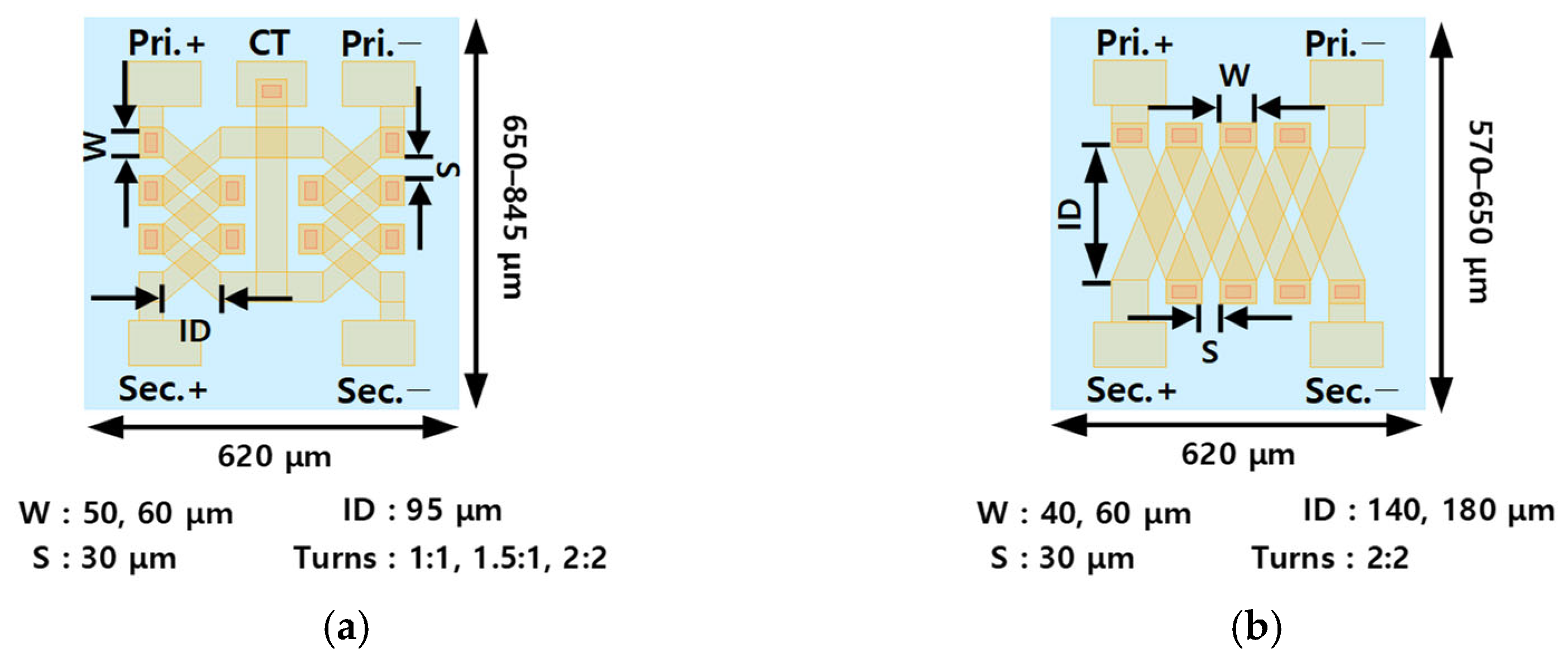
Figure 3a shows the dimensions of the 5-port transformer. The transformer has a center tap between the two coupled coils, with an inner diameter (ID) of 95 μm. The transformer has six variants: metal widths (Ws) of 50 and 60 μm and turns ratios of 1:1, 1.5:1, and 2:2. The total size of the 5-port transformers is a width of 620 μm and a length ranging from 650 to 845 μm.
The 4-port transformer has a single pair of coupled coils, as shown in Figure 3b, with inner diameters of 140 or 180 μm. Width options were 40 and 60 μm, so four variants were designed and fabricated. The overall size of the transformers is a width of 620 μm and a length ranging from 570 to 650 μm.
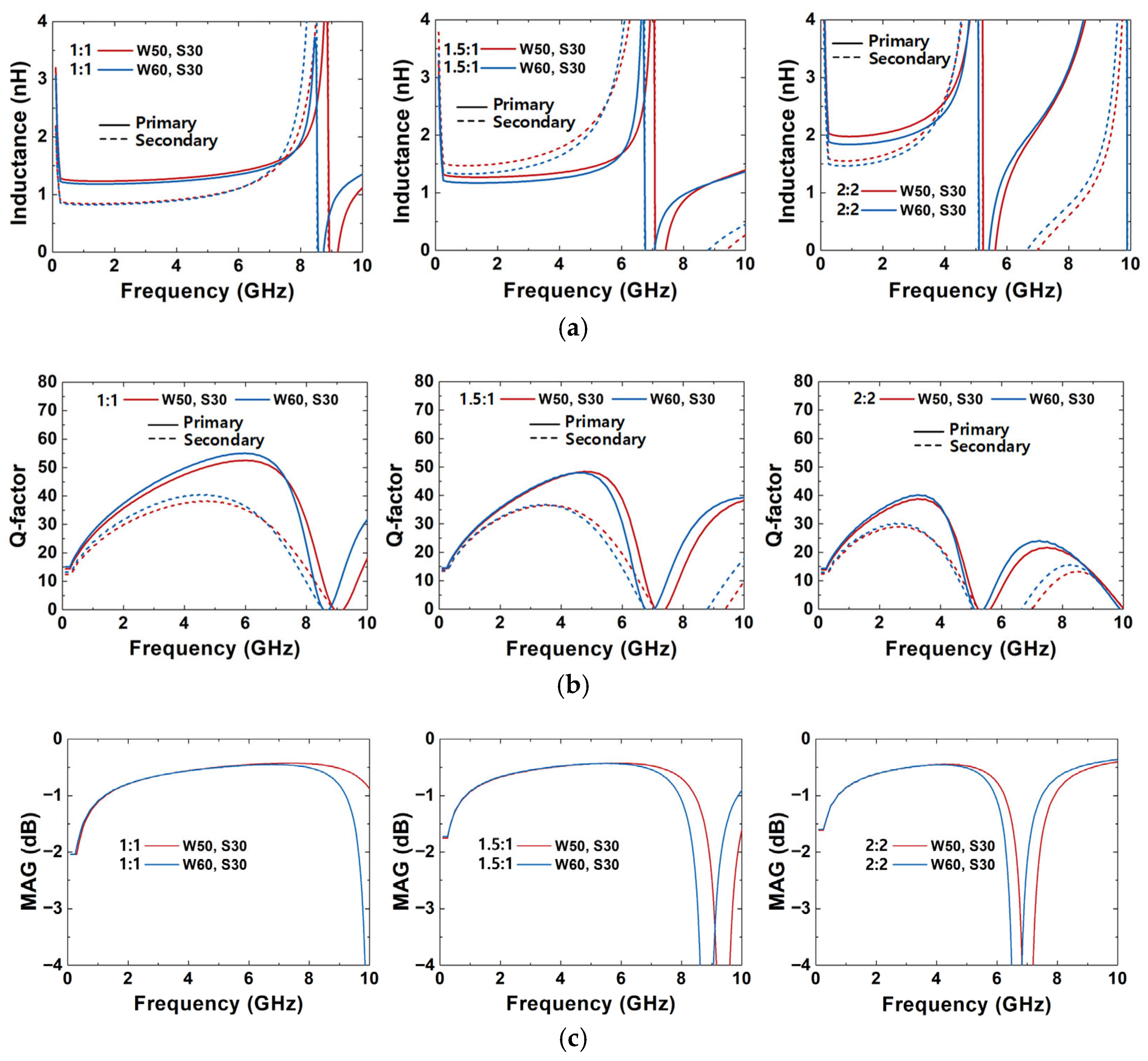
The characteristics of the center-tapped transformers are shown in Figure 4 and Table 1. There are a total of six center-tapped transformers, with three turn-ratio types (1:1, 1.5:1 and 2:2) and two winding-width variations (50 μm, 60 μm). The reference frequency for these values is 3.5 GHz, which is the target frequency in this work.
The inductance versus frequency characteristics of the transformers are shown in Figure 4a. The primary winding inductances range from 1.21 nH to 2.33 nH, and the secondary inductances range from 869.7 pH to 2.17 nH.
Thanks to the proposed structure, Q factors of primary windings range from 38.7 to 47.3, significantly higher than those of integrated transformers. Secondary-winding Q values are slightly lower (26.8 to 38.9) than the primaries, yet remain much higher than on-chip counterparts. Overall Q versus frequency is shown in Figure 4b.
The maximum available gain (MAG) results, which indicate the minimum loss of the transformers, are shown in Figure 4c. All six transformers exhibit low loss, consistent with their high-Q properties: MAG is no worse than −0.60 dB across all cases, with the best being −0.47 dB.
The 4-port transformers without a center-tap are also evaluated, as shown in Figure 5 and Table 2. With a symmetric, fully coupled structure, both the primary and secondary windings have the same properties, with improved Q and lower loss compared with center-tapped transformers. Four types of symmetric transformers without a center tap were evaluated, with width variations of 40 μm and 60 μm and inner diameters of 140 μm and 180 μm. All four transformers have a 2:2 turn ratio.
Figure 5a shows that the transformer inductances—primary and secondary—are nearly equal with the symmetric structures. The winding inductances range from 852.3 pH to 1.10 nH.
The Q factors are higher than those of the center-tapped transformers, as expected, ranging from 46.9 to 55.2 for both windings. These results indicate that the fully coupled symmetric structure is important for securing high-Q characteristics in differential operation. Detailed results are shown in Figure 5b.
The MAG is also better than that of the center-tapped transformers, with −0.39 to −0.32 dB achieved, as shown in Figure 5c.

3. Design of Power Amplifier with High-Q Glass Transformer

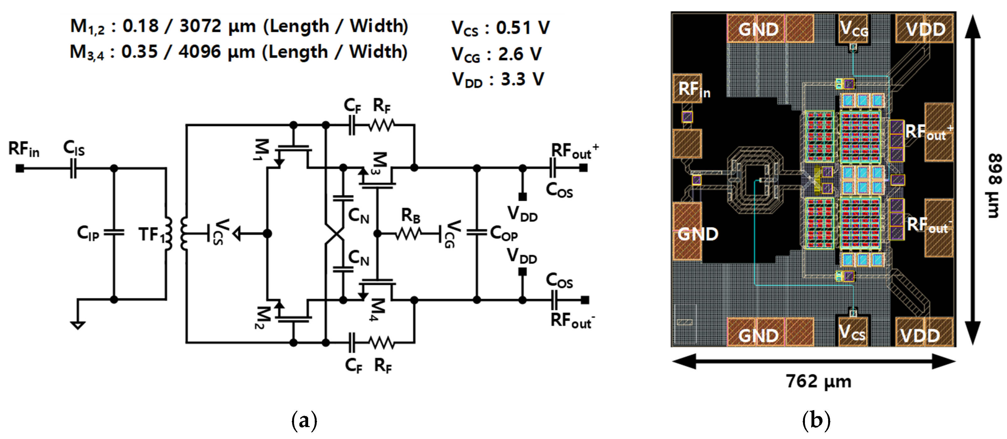
This section presents the design of a power amplifier composed of a CMOS differential PA core and an off-chip high-Q glass transformer, connected on a PCB, where the transformer provides the output-matching network. The PA core was fabricated with a 0.18 μm CMOS process. To verify the advantage of the high-Q transformer, the PA core has no on-chip output-matching network components and provides two differential pads, which are connected directly to the drains through series DC-blocking capacitors. Figure 6a shows the schematic and key specifications of the PA, with all components integrated except the output-matching network. The PA is based on a conventional differential cascode structure incorporating neutralization capacitors and RC feedback to ensure stability [23,24,25]. The common source transistors have a total gate width of 3072 μm and a gate length of 0.18 μm, while the common-gate transistors have a total gate width of 4096 μm and a gate length of 0.35 μm. The entire structure operates from a 3.3 V supply.
The PA core area, excluding the output-matching network, is 762 μm × 898 μm, as shown in Figure 6b. The detailed component values of the PA are summarized in Table 3.
Two output-matching networks are compared in this section: one composed of an integrated on-chip transformer and the other employing an external off-chip transformer. Figure 7 shows the dimensions of the employed transformers. The on-chip transformer is designed with a 1:2 turn ratio with a single-turn primary with a 35 μm metal line width and a two-turn secondary with a 20 μm metal line width, resulting in an overall area of 481 μm × 600 μm. The off-chip transformer has a 1:1 turn ratio with two-turn primary and secondary windings, each with a metal line width of 30 μm, and has overall dimensions of 570 μm × 620 μm. Despite being realized as an external component, the off-chip transformer occupies a footprint only about 22.45% larger than the on-chip counterpart.
In RF transformer design, to match the network to the target impedance, the inductance of the windings is mainly considered. The inductances of the transformers are shown in Figure 8a. The on-chip transformer has inductances of 2.2 nH (primary) and 0.67 nH (secondary). While the off-chip transformer has a 1:1 turn ratio, both windings have an inductance of 0.85 nH.
In addition to inductance, the winding length should be considered to achieve tight coupling. In general, a longer coupled line length is required at lower frequencies because the signal wavelength is longer. This trend can be verified using the maximum available gain (MAG). As shown in Figure 8c, the MAG drops markedly at lower frequencies. The on-chip transformer is optimized to minimize loss in the 3–4 GHz band and exhibits a MAG of −1.45 dB at 3.5 GHz. The off-chip transformer has its loss optimum above 3.5 GHz but still shows a much lower loss of 0.37 dB at 3.5 GHz, which is 1.08 dB lower than that of the on-chip transformer.
These results show that the Q factor is a key metric indicating transformer performance. When a transformer has a low Q factor, it not only exhibits high winding loss but also suffers from poor coupling. As shown in Figure 8b,c, the MAG of the high-Q transformer at low frequencies is much higher, and the minimum Q exceeds the peak Q of the integrated transformer, indicating that a high Q enables tighter coupling between the windings.
To practically compare the characteristics of on-chip and off-chip transformers, the large-signal matching impedance of the PA was evaluated through load-pull simulation at a frequency of 3.5 GHz. As shown in Figure 9a, the optimum load impedance for maximum PAE is 6.1 + j9.8 Ω, and both the on-chip and off-chip matching networks are matched to this impedance point for comparison under the same conditions.
Unlike the integrated transformer, the matching network of the off-chip transformer, illustrated in Figure 9b, was designed with the additional effects of bond wires taken into account.
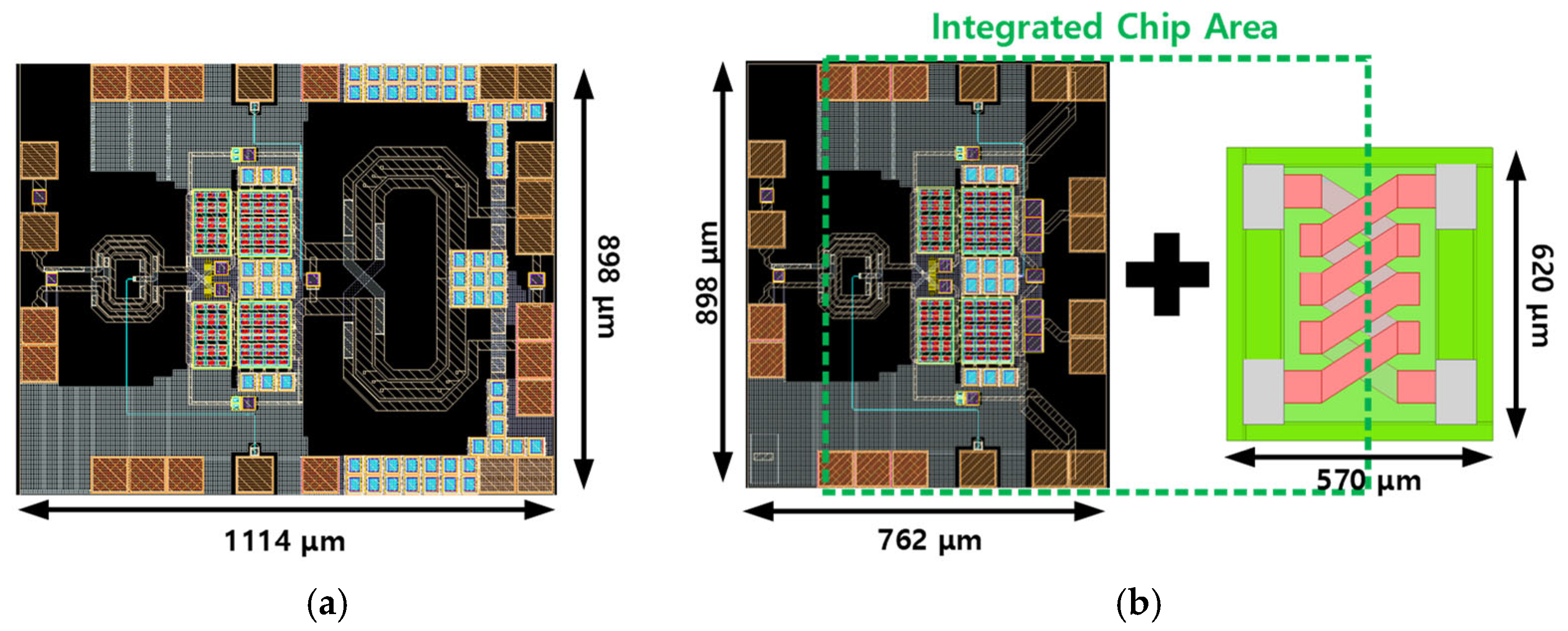
To compare the performance of the two types of transformers applied in actual PAs with simulations, a PA with the on-chip transformer was also designed. As shown in Figure 10, the PA with the external glass transformer maintains a compact footprint comparable to that of the fully integrated design. The fully integrated PA has a width of 1114 μm, while the PA with external matching and the proposed transformer has a width of 1332 μm, which is only 218 μm larger. If the external transformer is placed close to the PA output, the entire footprint could be approximately the same as that of the fully integrated PA.
While the Q of a matching network indicates both passband flatness and loss, if the network has a high-Q property, it exhibits narrower bandwidth but lower insertion loss than a low-Q network [26,27]. This means that by designing the network with a high Q, better performance can be achieved in the target frequency band. As shown in Figure 11a, the gain bandwidth of the proposed PA is narrower than that of the fully integrated PA, but it has slightly higher gain at the center frequency. Power and efficiency performance are also increased: saturation power (PSAT) increased by about 1.7 dBm, from 28.1 dBm to 29.8 dBm, and peak PAE improved by 11 percentage points, from 32.1% to 43.1%. These simulation results indicate that the high-Q transformer can significantly improve performance due to its low loss behavior, without a considerable increase in the overall PA size.

4. Assembly and Measurement of Power Amplifier with High-Q Glass Transformer

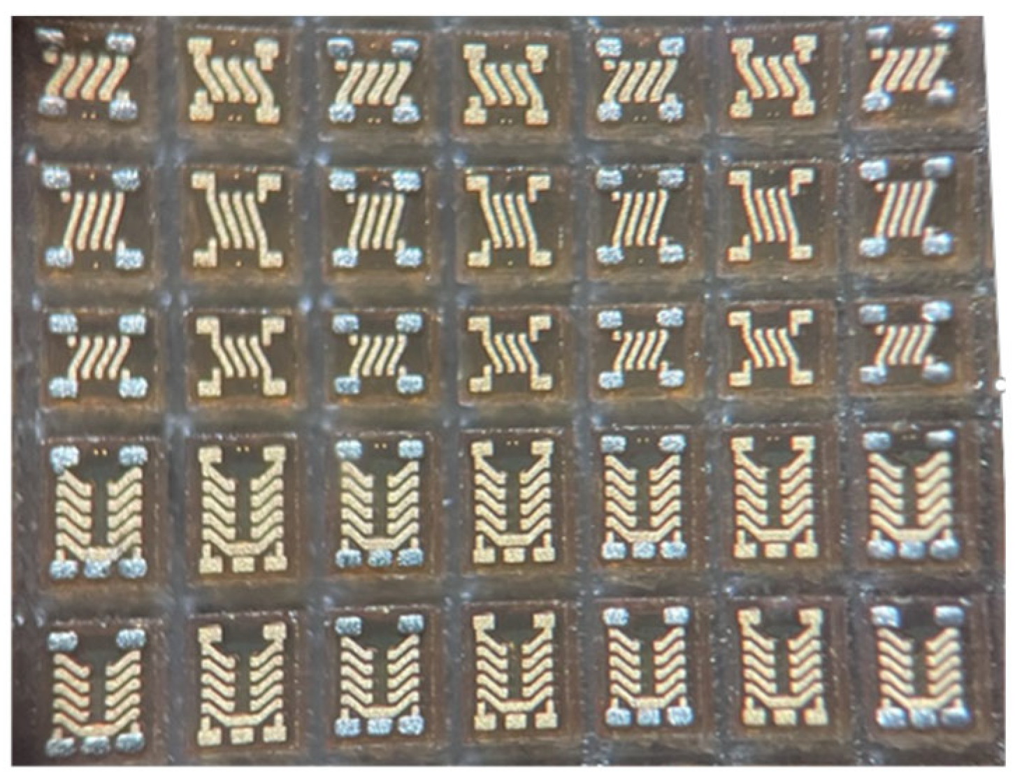
To verify the PA with a compact hybrid configuration, which was implemented with an integrated CMOS PA and a high-Q glass transformer, the PA was assembled on a PCB. The fabricated high-Q glass transformers are shown in Figure 12.
The PCB material was FR-4, which was appropriate for operation at 3.5 GHz. To achieve compactness, the PA and the transformer were placed as closely as possible, considering wire bonding and despite a height gap between the PA and the transformer. If the PA were ground to a proper height of nearly 300 μm or if more advanced assembly (including production-grade wire bonding) were applied, the bond-wire length could be shorter, and the overall size would be more compact, approaching the size of a fully integrated circuit. The assembled PA is shown in Figure 13.
While bond-wire inductance is part of the output-matching network, the length of the bond wire should be considered carefully. To verify the wire length effect, two DUTs were assembled, one with a longer bond wire and the other with a shorter one, as shown in Figure 14. Bond-wire inductance was assumed to be 500 pH for the primary and 400 pH for the secondary when designing the output-matching network.
In the measurements, the power optimum frequency shifted from 3.5 GHz to 2.9 GHz, and power and efficiency performance degraded by additional bond-wire inductance driven by the large height gap between the PA and the transformer as well as laboratory-level assembly limitations that prevented the achievement of a shorter bond-wire length. Comparing the measurement results of the samples in Figure 14a,b, as the bond-wire becomes shorter, the measurements move closer to the simulations in terms of S parameters, power, and efficiency. As shown in Figure 15a, for S21 of the PA, the longer bond wire has a peak gain of 12.3 dB at 3.04 GHz and the shorter bond wire has a peak gain of 13.9 dB at 3.43 GHz, a shift of +0.39 GHz, while the simulated peak gain is 17.7 dB at 3.8 GHz. For large-signal measurements, similar to the S-parameter trend, the measured results move closer to the simulations. In Figure 15b, the shorter bond wire achieves 25.3 dBm, which is 1.3 dBm higher than that with the longer bond wire and is closer to the simulation result of 29.8 dBm. The measured peak PAE also increased as the bond-= wire shortened, from 10.2% to 16.1%, while the simulation result was 43.1%, as shown in Figure 15c. These results are summarized in Table 4.
Due to performance degradation caused by bond wires that were longer than expected, modulated-signal results were inferred from simulation, assuming a 6 dB back-off, as is typical for a conventional class-AB PA. The expected average output power and average efficiency at an EVM of −25 dB (≈5.64%) are 22.18 dBm and 24.43%, respectively.
Table 5 shows a summary of the designed PA performance and a comparison with various CMOS PAs. As discussed earlier, the minimum achievable bond-wire length degraded the measured performance and masked the high-Q transformer’s performance improvement. Therefore, simulation results are presented to clearly demonstrate the performance gains. As shown by the figure of merit (FoM) for power and efficiency normalized by area, the high-Q transformer demonstrates a significant benefit in simultaneously achieving size miniaturization and PA performance improvement.

5. Conclusions

This study verifies the utility of an ultra-compact high-Q transformer for sub-6 GHz operation through simulation and fabrication, followed by validation in real-world operation when deployed as an off-chip output-matching network for a CMOS-integrated PA. While a fully integrated CMOS PA offers compactness suitable for ultra-small devices, it suffers from relatively low performance, including power efficiency; therefore, the high-Q glass transformer fabricated in this study is a promising alternative, anticipated to substantially improve the PA’s overall performance without a considerable increase in the overall circuit area. The transformer was fabricated using a photosensitive glass etching process and features high-aspect-ratio double-sided interconnects. Before fabrication, optimum winding width, spacing, the number of turns, and other parameters for sub-6 GHz PA load-pull impedance were identified using electromagnetic (EM) simulations. The simulation results show that the high-Q glass transformer can provide significantly improved performance when applied to the PA, especially in output power and efficiency compared with a fully integrated output transformer. The saturated output power increased by 1.7 dB from 28.1 to 29.8 dBm, and the peak PAE improved by 11 percentage points, from 32.1 to 43.1%. After the PA and transformers were fabricated, multiple PAs were assembled to mitigate uncertainty from the bond-wire inductance, which directly affects output-matching impedance as well as process variation in the core PA. The measurement results showed a clear trend: as the bond wire shortened, the measurements became closer to the simulation results. Improved results are expected if the PA substrate is ground to a height near that of the fabricated transformers (≈300 μm) and the assembly uses production-grade processes. The compact high-Q transformers, both as a standalone concept and when combined with a CMOS PA, demonstrate the feasibility of achieving miniaturization and high performance together.

Author Contributions

Conceptualization, J.L. and J.-M.Y., and C.P.; methodology, J.L., J.-M.Y., and J.Y.; investigation, J.L. and J.-M.Y.; supervision, C.P.; writing—original draft, J.L.; review and editing, C.P. All authors have read and agreed to the published version of the manuscript.

Funding

This work was supported by the Institute of Information & Communications Technology Planning & Evaluation (IITP) grant funded by the Republic of Korea government (Ministry of Science and ICT, MSIT) under grant RS-2024-00395702.

Data Availability Statement

All the material in this study is mentioned in this article.

Acknowledgments

The EDA tool was supported by the IC Design Education Center (IDEC), Republic of Korea.

Conflicts of Interest

The authors declare no conflicts of interest.

References

  1. Yue, C.P.; Wong, S.S. On-Chip Spiral Inductors with Patterned Ground Shields for Si-Based RF ICs. IEEE J. Solid-State Circuits 1998, 33, 743–752. [Google Scholar] [CrossRef]
  2. Mohan, S.S.; del Mar Hershenson, M.; Boyd, S.P.; Lee, T.H. Simple Accurate Expressions for Planar Spiral Inductances. IEEE J. Solid-State Circuits 1999, 34, 1419–1424. [Google Scholar] [CrossRef]
  3. Chen, H.-H.; Hsu, Y.-W. Analytic Design of on-Chip Spiral Inductor with Variable Line Width. Electronics 2022, 11, 2029. [Google Scholar] [CrossRef]
  4. Jang, J.; Park, C.; Kim, H.; Hong, S. A CMOS RF Power Amplifier Using an Off-Chip Transmission Line Transformer With 62% PAE. IEEE Microw. Wireless Compon. Lett. 2007, 17, 385–387. [Google Scholar] [CrossRef]
  5. Lim, W.; Kang, H.; Lee, W.; Bae, J.; Oh, S.; Oh, H.; Chae, S.; Hwang, K.-C.; Lee, K.-Y.; Yang, Y. Dual-Mode CMOS Power Amplifier Based on Load-Impedance Modulation. IEEE Microw. Wireless Compon. Lett. 2018, 28, 1041–1043. [Google Scholar] [CrossRef]
  6. Chiou, H.-K.; Lin, H.-C.; Chang, D.-C. High-Efficiency and Cost-Effective 10 W Broadband Continuous Class-J Mode Quasi-MMIC Power Amplifier Design Utilizing 0.25 μm GaN/SiC and GaAs IPD Technology for 5G NR n77 and n78 Bands. Electronics 2023, 12, 3494. [Google Scholar] [CrossRef]
  7. Eid, M.A.E.; Abouelnaga, T.G.; Ibrahim, H.A.; Hamad, E.K.I.; Al-Gburi, A.J.A.; Alghamdi, T.A.H.; Alathbah, M. Highly Efficient GaN Doherty Power Amplifier for N78 Sub-6 GHz Band 5G Applications. Electronics 2023, 12, 4001. [Google Scholar] [CrossRef]
  8. Que, X.; Li, J.; Wang, Y. A Broadband Three-Way Series Doherty Power Amplifier with Deep Power Back-Off Efficiency Enhancement for 5G Application. Electronics 2024, 13, 1882. [Google Scholar] [CrossRef]
  9. Angarita Malaver, E.F.; Barrera Lombana, N.; Moreno Rubio, J.J. Smith Chart-Based Design of High-Frequency Broadband Power Amplifiers. Electronics 2024, 13, 4096. [Google Scholar] [CrossRef]
  10. Vasjanov, A.; Barzdenas, V. A Review of Advanced CMOS RF Power Amplifier Architecture Trends for Low Power 5G Wireless Networks. Electronics 2018, 7, 271. [Google Scholar] [CrossRef]
  11. Lee, M.; Yoo, J.; Lee, J.; Park, C. Design Techniques for Wideband CMOS Power Amplifiers for Wireless Communications. Electronics 2024, 13, 1695. [Google Scholar] [CrossRef]
  12. Wang, Z.; Wang, X.; Liu, Y. A Wideband Power Amplifier in 65 nm CMOS Covering 25.8–36.9 GHz by Staggering Tuned MCRs. Electronics 2023, 12, 3566. [Google Scholar] [CrossRef]
  13. Wu, C.-H.; Tang, C.-C.; Liu, S.-I. Analysis of On-Chip Spiral Inductors Using the Distributed Capacitance Model. IEEE J. Solid-State Circuits 2003, 38, 1040–1044. [Google Scholar] [CrossRef]
  14. Jiang, H.; Yeh, J.L.A.; Tien, N.C. On-Chip Spiral Inductors Suspended over Deep Copper-Lined Cavities. IEEE Trans. Microw. Theory Tech. 2000, 48, 2415–2423. [Google Scholar] [CrossRef]
  15. Goñi, A.; del Pino, J.; González, B.; Hernández, A. An Analytical Model of Electric Substrate Losses for Planar Spiral Inductors on Silicon. IEEE Trans. Electron Devices 2007, 54, 546–553. [Google Scholar] [CrossRef]
  16. Ye, W.; Ma, K.; Yeo, K.S.; Zou, Q. A 65 nm CMOS Power Amplifier with Peak PAE above 18.9% from 57 to 66 GHz Using Synthesized Transformer-Based Matching Network. IEEE Trans. Circuits Syst. I Regul. Pap. 2015, 62, 2533–2543. [Google Scholar] [CrossRef]
  17. Estrada, J.A.; Montejo-Garai, J.R.; de Paco, P.; Psychogiou, D.; Popović, Z. Power Amplifiers with Frequency-Selective Matching Networks. IEEE Trans. Microw. Theory Tech. 2021, 69, 697–708. [Google Scholar] [CrossRef]
  18. Wei, Z.; Huang, F.; Zhang, Y.; Tang, X.; Jiang, N. A Compact Transformer-Based E-Band CMOS Power Amplifier with Enhanced Efficiencies of 15.6% PAE1dB and 6.5% PAE at 6 dB Power Back-Off. Electronics 2022, 11, 1679. [Google Scholar] [CrossRef]
  19. Kim, M.S.; Pulugurtha, M.R.; Sundaram, V.; Tummala, R.R.; Yun, H. Ultrathin High-Q 2-D and 3-D RF Inductors in Glass Packages. IEEE Trans. Compon. Packag. Manuf. Technol. 2018, 8, 643–652. [Google Scholar] [CrossRef]
  20. Wu, X.; Wen, L.; Cao, L.; Cao, G.; Li, G.; Fu, Y.; Yu, Z.; Fang, Z.; Wang, Q. A Fully Integrated Solid-State Charge Detector with Through Fused Silica Glass Via Process. Electronics 2023, 12, 1045. [Google Scholar] [CrossRef]
  21. Huang, T.-J.; Kiebala, T.; Suflita, P.; Moore, C.; Housser, G.; McMahon, S.; Puchades, I. Comparative Analysis of Thermal Properties in Molybdenum Substrate to Silicon and Glass for a System-on-Foil Integration. Electronics 2024, 13, 1818. [Google Scholar] [CrossRef]
  22. Galler, T.; Chaloun, T.; Mayer, W.; Kröhnert, K.; Ambrosius, N.; Schulz-Ruhtenberg, M.; Waldschmidt, C. MMIC-to-Dielectric Waveguide Transitions for Glass Packages above 150 GHz. IEEE Trans. Microw. Theory Tech. 2023, 71, 2807–2817. [Google Scholar] [CrossRef]
  23. Park, J.; Lee, C.; Yoo, J.; Park, C. A CMOS Antiphase Power Amplifier with an MGTR Technique for Mobile Applications. IEEE Trans. Microw. Theory Tech. 2017, 65, 4645–4656. [Google Scholar] [CrossRef]
  24. Kim, T.; Park, C. Ka-Band Three-Stacked CMOS Power Amplifier with LC Shunt-Feedback to Enhance Gain and Stability. IEEE Trans. Circuits Syst. II Express Briefs 2024, 71, 1969–1973. [Google Scholar] [CrossRef]
  25. Asada, H.; Matsushita, K.; Bunsen, K.; Okada, K.; Matsuzawa, A. A 60 GHz CMOS Power Amplifier Using Capacitive Cross-Coupling Neutralization with 16% PAE. In Proceedings of the 41st European Microwave Conference (EuMC), Manchester, UK, 10–13 October 2011; pp. 1115–1118. [Google Scholar]
  26. Wu, H.; You, B.; Gao, K.-K.; Li, X.-G. A 4th-Order LTCC Bandpass Filter with Both Tunable Center Frequency and Bandwidth. Electronics 2022, 11, 4119. [Google Scholar] [CrossRef]
  27. Espinosa-Adams, D.; Llorente-Romano, S.; González-Posadas, V.; Jiménez-Martín, J.L.; Segovia-Vargas, D. Novel Dielectric Resonator-Based Microstrip Filters with Adjustable Transmission and Equalization Zeros. Electronics 2025, 14, 2557. [Google Scholar] [CrossRef]
  28. Tsai, J.-H. A 5.3-GHz 30.1-dBm Fully Integrated CMOS Power Amplifier with High-Power Built-In Linearizer. IEEE Microw. Wirel. Technol. Lett. 2023, 33, 431–434. [Google Scholar] [CrossRef]
  29. Ginzberg, N.; Cohen, E. A Wideband CMOS Power Amplifier With 52% Peak PAE Employing Resistive Shunt Feedback for Sub-6 GHz 5G Applications. IEEE Microw. Wirel. Technol. Lett. 2023, 33, 192–195. [Google Scholar] [CrossRef]
  30. Lin, H.-C.; Liao, H.-Z.; Chang, D.-C.; Chiou, H.-K. A Highly Linear Stacked CMOS Power Amplifier with Cold-FET Linearizer for Sub-6 GHz Applications. In Proceedings of the 2024 IEEE Asia-Pacific Microwave Conference (APMC), Bali, Indonesia, 17–20 November 2024; pp. 952–954. [Google Scholar] [CrossRef]
  31. Cancelli, R.; Avitabile, G.; Florio, A. Designing and Optimizing a 2.4 GHz Complementary Metal–Oxide–Semiconductor Class-E Power Amplifier Combining Standard and High-Voltage Metal–Oxide–Semiconductor Field-Effect Transistors. Electronics 2025, 14, 1135. [Google Scholar] [CrossRef]
Figure 1. Simplified PA assembled on PCB: (a) fully integrated, (b) hybrid with conventional external components, and (c) hybrid with proposed glass transformer.
Electronics 14 04261 g001
Figure 2. Structure of the high-Q glass transformer: (a) stack-up, (b) 4-port transformer, and (c) 5-port transformer.
Electronics 14 04261 g002
Figure 3. Dimensions of the two transformer types: (a) 5-port center-tapped transformer and (b) 4-port transformer.
Electronics 14 04261 g003
Figure 4. Simulation results of 5-port transformers: (a) inductance, (b) Q factor, and (c) MAG.
Electronics 14 04261 g004
Figure 5. Simulation results of 4-port transformers: (a) inductance, (b) Q factor, and (c) MAG.
Electronics 14 04261 g005
Figure 6. Designed CMOS power amplifier: (a) schematic and (b) layout.
Electronics 14 04261 g006
Figure 7. Output transformer layout: (a) CMOS-integrated transformer and (b) off-chip high-Q glass transformer.
Electronics 14 04261 g007
Figure 8. Simulation results of on-chip and off-chip transformers: (a) inductance, (b) Q factor, and (c) MAG.
Electronics 14 04261 g008
Figure 9. Output matching for the PA: (a) load-pull, (b) integrated transformer network, and (c) off-chip transformer network.
Electronics 14 04261 g009
Figure 10. Layout size: (a) fully integrated PA and (b) integrated core PA with off-chip transformer.
Electronics 14 04261 g010
Figure 11. Comparison of simulation results for on-chip and off-chip output-matched power amplifiers: (a) S parameters, (b) output power vs. power gain, and (c) PAE.
Electronics 14 04261 g011
Figure 12. Photographs of fabricated high-Q glass transformers.
Electronics 14 04261 g012
Figure 13. Photographs of the assembled PA: (a) entire PCB and (b) core PA with off-chip transformer.
Electronics 14 04261 g013
Figure 14. Two assembled PAs for bond-wire-length comparison: (a) long bond-wire configuration and (b) short bond-wire configuration.
Electronics 14 04261 g014
Figure 15. Performance trends versus bond-wire length: (a) S parameters, (b) output power vs. power gain, and (c) PAE.
Electronics 14 04261 g015
Table 1. Characteristics of 5-port transformer at 3.5 GHz.
TurnsWidthInductance
(Primary)
Inductance
(Secondary)
Q Factor
(Primary)
Q Factor
(Secondary)
MAG
1:150 μm1.26 nH886.0 pH45.236.5−0.60 dB
60 μm1.21 nH869.7 pH47.338.9−0.47 dB
1.5:150 μm1.32 nH1.67 nH44.638.9−0.51 dB
60 μm1.22 nH1.53 nH45.036.8−0.51 dB
2:250 μm2.33 nH2.17 nH38.726.5−0.47 dB
60 μm2.16 nH2.06 nH40.026.8−0.47 dB
Table 2. Characteristics of 4-port transformers at 3.5 GHz.
WidthDiam.Inductance
(Primary)
Inductance
(Secondary)
Q Factor
(Primary)
Q Factor
(Secondary)
MAG
40 μm140 μm975.7 pH969.8 pH46.946.9−0.39 dB
180 μm1.10 nH1.09 nH50.950.6−0.35 dB
60 μm140 μm852.3 pH846.0 pH52.352.4−0.37 dB
180 μm935.4 pH931.2 pH54.555.2−0.32 dB
Table 3. Component values used in the PA.
ComponentValueComponentValue
CIS884.8 fFCN803.6 fF
CIP517.8 fFCF1.90 pF
COP1.20 pFRF607.1 Ω
COS2.85 pFRB2 kΩ
Table 4. Comparison between measured results (bond-wire variations) and simulations.
ParameterLong Bond WireShort Bond WireSimulation
S21,PEAK (dB)12.3 @3.04 GHz13.9 @3.43 GHz17.7 @3.8 GHz
PSAT (dBm)24.0 @2.9 GHz25.3 @2.9 GHz29.8 @3.5 GHz
PAEPEAK (%)10.2 @2.9 GHz16.1 @2.9 GHz43.1 @3.5 GHz
Table 5. Performance comparison with state-of-the-art CMOS PAs.
Ref.Tech.Freq.
(GHz)
PSAT
(dBm)
PAE
(%)
Size
(mm2)
FoM 2
[28]0.18 μm5.330.1182.960.062
[29]65 nm0.33–2.519.5–21.535–52.40.490.151
[30]0.18 μm2.9–525.7–27.2≈15–253.700.035
[31] 10.13 μm2.420.540.90.6570.070
This work 10.18 μm3.529.843.11.20 30.343
1 Simulation results.; 2 FoM = (PSAT (W) × PAE) / size (mm2); 3 width: PA + transformer, height: PA.
Disclaimer/Publisher’s Note: The statements, opinions and data contained in all publications are solely those of the individual author(s) and contributor(s) and not of MDPI and/or the editor(s). MDPI and/or the editor(s) disclaim responsibility for any injury to people or property resulting from any ideas, methods, instructions or products referred to in the content.