Abstract
Improving the transient response performance is a critical challenge in low-dropout regulator (LDO) design. This paper proposes a novel on-chip capacitor-less LDO based on substrate technology implemented in an SMIC (Semiconductor Manufacturing International Corporation) 0.18 μm CMOS (complementary metal oxide semiconductor technology) process. Central to this innovation is a fast response loop between the PMOS driver’s body and gate, which leverages the body effect to enhance driver control without complex bulk-driven techniques. The proposed LDO achieves a quiescent current of 4.5 μA, an efficiency of , an overshoot/undershoot of , and a settling time of 1.2 μs. The comparative analysis confirms that this structure increases the maximum load current and reduces the loop response time relative to those for conventional LDOs. These results validate a significant improvement in the transient performance, marking an important advance in integrated voltage regulator technology.
1. Introduction
Recent advancements in information technology have enabled the ubiquitous deployment of electronic instruments across diverse domains. Innovations in artificial intelligence, the Internet of Things (IoT), and 5G technology are driving the evolution of electronic systems towards enhanced performance and miniaturization. Within these systems, power management modules are indispensable, with low-dropout linear regulators (LDOs) serving as critical components.
LDOs are broadly categorized into two types: conventional LDOs requiring external capacitors and capacitor-less LDOs. The former necessitate larger external capacitors to ensure system stability, which occupy a substantial circuit area, leading to an increased device footprint, a reduced integration density, and higher costs. In contrast, capacitor-less LDOs offer superior miniaturization, higher integration, and improved cost effectiveness. Consequently, designing capacitor-less LDOs with a fast transient response holds significant value in applications demanding low supply voltages, particularly where an ultra-low quiescent current and the elimination of external capacitors are critical. Such scenarios include IoT sensor nodes, medical implants, and portable medical monitors, where stringent power efficiency constraints and extreme miniaturization requirements are paramount.
In existing reports, many scholars have proposed various methods to enhance the transient response of capacitor-less LDOs. Reference [1] introduces an enhanced multi-path nested Miller compensation (EMNMC) scheme that achieves a loop bandwidth exceeding 100 MHz, but its static current is as high as 112 μA, which fails to meet low power requirements. In 2019, reference [2] designed a class AB error amplifier and adopted a power transistor current enhancement structure. The LDO had a response time of 220 ns during a 100 ns load transition from 1 mA to 100 mA, indicating that the slope enhancement circuit did not significantly improve the response speed of the LDO. Reference [3] designed a capacitance-free LDO aimed at enhancing the frequency compensation stability and proposed a dual active feedback frequency compensation scheme. Although the static current is 14 μA, which meets the requirements in terms of the stability and transient response, its response time is as long as 3.2 μs, which fails to meet the requirement of a fast response. In 2021, reference [4] introduced a low-power fast-transient-response LDO based on a super transconductance structure. During the edge time of the maximum change in the load current of 20 ns, the peak output voltage is less than 11.2 mV, and the response time is 0.054 μs. However, its static current is as high as 124 μA, and the LDO also requires an additional external large capacitor to ensure system stability. These studies generally indicate that the existing methods predominantly enhance the performance by incorporating additional circuit structures at the gate terminals of the power transistors, such as augmenting transient circuits to increase charge and discharge currents [5,6]. However, this approach inevitably leads to increased circuit power consumption and a larger chip area and fails to address the low-voltage-difference problem [7,8]. The shortcomings of these conventional methods are that they either necessitate a trade-off in the bandwidth or response speed at the expense of an elevated static current or fail to provide a fundamental solution for achieving a fast response under low-voltage conditions. Consequently, a more optimized solution is urgently required.
This study mainly explores the scientific issues in substrate-driven capacitor-less LDOs, clarifies the high-power-consumption problem in the fast response circuit module structure of an LDO, and proposes a novel substrate-driven enhanced-transient-response LDO structure, as shown in Figure 1. Taking PMOS power transistors as an example for the analysis, two loops are formed by adding substrate driving loops. The main loop ensures a high loop gain to maintain the accuracy of the output voltage, while the substrate loop has a higher loop bandwidth to shorten the loop stabilization time. The substrate terminal of the power transistor driven by the substrate amplifier is biased in the same direction as the gate terminal to reduce the threshold voltage of the PMOS transistor. This enables operation at lower supply voltages, increases the overdrive voltage, facilitates a larger current handling capability, and ultimately improves the transient characteristics. Based on an analysis of the existing methods’ shortcomings, this study aims to provide an effective approach to achieving a fast transient response with low power consumption.
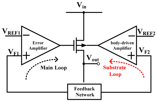
Figure 1.
Schematic of substrate-driven capacitor-less LDO architecture.
The rest of this article is arranged as follows: Section 2 introduces the basic structure of an LDO and the details of each module. Section 3 provides a detailed introduction to the design of an LTE-LDO circuit system based on substrate driving technology. Section 4 describes the layout design and overall layout arrangement and analyzes simulation verification data of the DC characteristics, AC characteristics, and transient characteristics of the circuit in detail. The results are quantified as quality factors and compared with other research results. Section 5 provides an overview and summary of all of the work presented in this paper.
2. An Overview of a Typical LDO
As shown in Figure 2, the diagram illustrates the typical structure of the basic modules of an LDO [9].
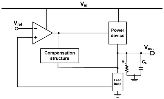
Figure 2.
A schematic diagram of a typical LDO Structure.
As an important part of the voltage regulator, the LDO can stabilize the output voltage under different input voltages and output currents [10,11]. When the output stage circuit switches from the standby state to the working state, the discharge of the load capacitor will cause the output voltage to decrease, and the feedback signal is provided to the positive input of the error amplifier through the resistance voltage divider feedback network [12,13]. Compared with the reference voltage, the output signal of the error amplifier is adjusted, and then the power tube is driven to generate more current, and finally, the output voltage of the LDO is raised. Similarly, when the output stage circuit switches from the working state to the standby state, the excess charge will charge the load capacitor to increase the output voltage [14]. The feedback signal is transmitted to the input of the error amplifier through the feedback network and compared with the reference voltage; the output signal of the amplifier is adjusted; and the power device is driven to reduce the external current and reduce the output voltage of the LDO [15]. Figure 2 shows an equivalent working schematic diagram of the LDO. The power device is equivalent to the adjustable resistance of , and the load and feedback network are equivalent to the impedance of and . The power resistance is adjusted by dynamically adjusting the feedback voltage () to complete the voltage regulation process.
3. The Proposal Substrate-Driven LTE-LDO
3.1. The Overview
This section elaborates on the implementation of substrate-driven technology in analog integrated circuits, focusing on the proposed LTE-LDO (low-power transient-enhanced low-dropout regulator). Conventional fast-transient-response LDO architectures typically incorporate slew-rate enhancement circuits, fast feedback loops, error amplifiers, and over-/undershoot detection modules. Departing from the established approaches, we propose a novel capacitor-less topology that eliminates the off-chip capacitance requirements. The key innovation lies in the integration of a substrate-driven fast-response loop, which applies same-direction biasing to both the gate and substrate terminals of the power transistor. This configuration reduces the threshold voltage and enhances the transconductance, thereby improving the current handling capability and transient performance. Figure 3 presents a system block diagram of the LTE-LDO architecture.
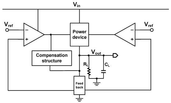
Figure 3.
The LTE-LDO diagram designed in this section.
Figure 4 presents a schematic diagram of the core circuit structure of the LTE-LDO designed in this section. The complete circuit consists of the main error amplifier, the substrate amplifier, and the power stage. To ensure high loop gain in the main loop, a super AB-class transconductance amplifier is used as the main error amplifier. To ensure the stability of the main loop, a compensation structure is also added to the main loop. The substrate loop employs a five-transistor amplifier structure to increase the loop bandwidth and reduce the loop response time.
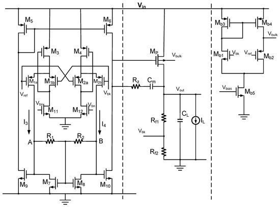
Figure 4.
A schematic of the core circuit of the LTE-LDO.
3.2. The Main Error Amplifier
A folded cascode amplifier (FC) is often used in the error amplifier structure in LDO design. This traditional error amplifier is widely used and has a stable structure. However, its tail current source leads to a limited range of current variation at the gate of the power tube and low charging and discharging currents. In order to solve this problem, JuAn A. Galan et al. proposed the class transconductance amplifier OTA [16]. This structure can drive the power transistor in the LDO through the adaptive bias current of the input transistor; to maximize the current efficiency, it can achieve a high output voltage swing at a low static current; and it can improve the slew rate (SR) of the amplifier, increase the charge and discharge currents of the power tube gate, and, finally, improve the transient characteristics of the LDO. In addition, the equivalent resistance at the output of the amplifier is low, which will bring a poor loop gain. In order to improve the gain and achieve a good adjustment rate, this paper adds the local common-mode feedback (LCMFB) structure based on the class OTA circuit. It can be increased to the original circuit R times so as to effectively improve the adjustment rate. A detailed comparative quantitative analysis of the performance of the three amplifiers is presented below.
3.2.1. The Slew Rate
Figure 5a shows a schematic of the complete circuit of the FC amplifier. It is represented by a tail current source composed of MOS transistors denoted as , where and are input transistors; , , , and form the cascode current mirror; and constitute cascode transistors; and and serve as current sources. , , and are the bias voltages for and , and , and and , respectively. The output voltage swing () of this amplifier can be expressed as
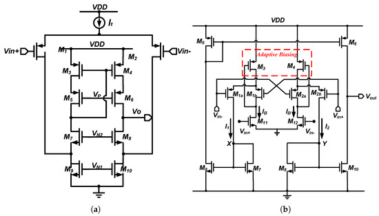
Figure 5.
A schematic comparison of the amplifier topologies: (a) a conventional folded cascode amplifier. (b) A classical class AB operational transconductance amplifier.
represents the overdrive voltage of the MOS transistor, and VDD denotes the power supply voltage of the amplifier.
Figure 5b provides a complete schematic of the class transconductance amplifier. The core consists of the adaptive bias current source formed by and , the input transistors and , and the fixed tail current source transistors and , with the remaining transistors and , and , and and serving as current mirror replication transistors. and act as output load transistors. The output voltage swing of this amplifier is
The output voltage swing rate of the amplifier is calculated as follows.
is the output current of the amplifier, is the load capacitance, and t is the settling time of the output.
In the SMIC 180 nm mmrf process, the overdrive voltage of the n33 series transistors is usually around 200 mV. As indicated by Equation (3), under the same power supply voltage conditions, the output swing of the class amplifier is significantly higher than that of the FC amplifier. In an LDO, when driving power transistors of the same size at the gate end, the charging and discharging currents of the former are greater than those of the latter. The working principle of the adaptive bias current source in this structure is as follows: when the output load current of the LDO changes, the output voltage is fed back to the input, increasing or decreasing the currents of and . Since and provide a fixed current source IB, the currents of and dynamically increase or decrease in the same manner. The changing current passes through , , , and to the output. In comparison to the FC amplifier, this output current is not limited by the bias current source, thereby significantly increasing the charging and discharging currents and benefiting an improvement in the transient response.
3.2.2. DC Gain
By analyzing the internal nodes of the amplifier in Figure 5b, it can be observed that due to the diode-connected configuration of and , points A and B are low-impedance nodes. The DC gain of this amplifier can be expressed as
and are the equivalent transconductances of and , respectively. represents the equivalent resistance between nodes X and Y. denotes the output impedance of the amplifier. Further analyzing the loop gain, can be approximated as and simplified to
represents the transconductance of . It can be seen that denotes the ratio of the current mirror. Clearly, without adding additional static current, the gain of traditional class amplifiers is limited by and cannot meet the requirements for high voltage regulation adjustment rates in low-power conditions in LDOs.
Therefore, to address this issue, the proposed LDO without off-chip large capacitors utilizes a super class error amplifier with local common-mode feedback [17].
As shown in Figure 6, a resistor is added in the red section on the basis of the traditional amplifier, increasing the AC impedance at points A and B while keeping the DC impedance unchanged, effectively boosting the amplifier’s gain. At this point, the DC gain of the amplifier can be expressed as
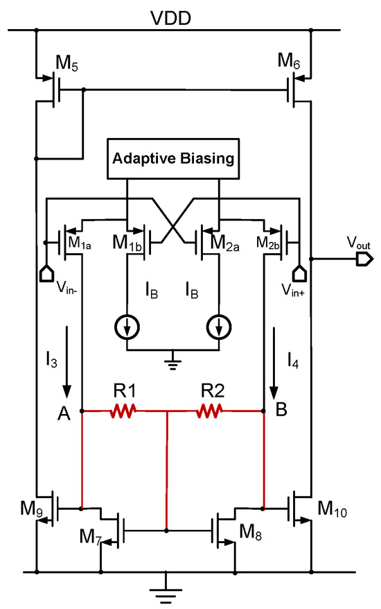
Figure 6.
Modified super class AB OTA with enhanced resistive network.
are the equivalent resistances at points A and B, serving as the feedback resistors used in LCMFB [18,19], significantly smaller than and . Combining the above expressions leads to the conclusion that compared to the traditional structure, adding feedback resistors does not consume additional static current, effectively enhancing the gain. However, should not be set too large, with values typically ranging between 400 k and 1 M; otherwise, this pole will shift to lower frequencies, resulting in a decreased phase margin and posing loop stability issues.
3.2.3. The Output Current
Compared to a traditional class transconductance amplifier, the amplifier shown in Figure 6 significantly enhances the charging and discharging currents at the gate of the power transistor. Next, a detailed quantitative analysis will be conducted [20].
Assuming both amplifiers are driving the same power transistor, when Figure 5 acts as the error amplifier, transitioning from a light load to a heavy load current in the LDO causes the output voltage to instantaneously drop by V. This change is fed back to the input of the amplifier, causing the gate voltages of and to decrease by a factor of times . Since the source voltage of is constant, the current flowing through , denoted as , increases. As the bias current is fixed, the source voltages of and also decrease, resulting in a decrease in the current flowing into , denoted as . Here, represents the feedback coefficient for output impedance voltage division. and can be represented as follows:
, appearing in all the expressions in this paper, is defined as
The power tube gate discharge current can be defined as follows.
When the output of the LDO without an off-chip large capacitor switches from a heavy load to a light load, overshoot voltage will be generated. At this time, the charging current of the power tube gate can be expressed as follows.
Compared to the traditional amplifier structure in Figure 5b, to enhance the switching speed of the power transistor’s gate, this paper employs an efficient error amplifier, as shown in Figure 6. When the proposed LDO generates an undershoot voltage , the current increases while decreases, causing an increase in the voltage at node A and a decrease in the voltage at node B. This results in an increase in the current flowing into M10 and a decrease in the current flowing into M10. Therefore, the charging current is described as
When an overshoot voltage is generated, the discharge current of the power tube can be defined as follows.
Through the large-signal analysis, it can be seen that compared with the traditional topology, when the error amplifier of super class drives the power tube under the same static power consumption, the output terminal can generate a fourth power charge and discharge current. Therefore, the structure shown in Figure 6 greatly increases the conversion rate of the power transistor gate, which greatly improves the transient response.
3.2.4. Small-Signal Analysis
Figure 7 shows the equivalent small-signal flow chart of the error amplifier proposed in this paper. There are a few caveats to the flow chart before calculating the system’s functions:
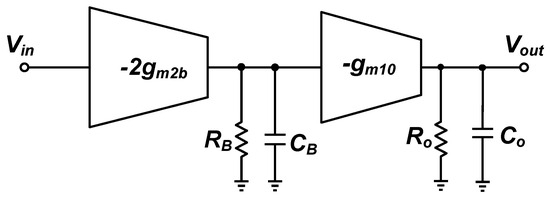
Figure 7.
Super class AB transconductance amplifier small signal flow chart.
- (1)
- There is a Flipped Voltage Follower (FVF) structure [21] in the amplifier. When the input tube changes , the branch of the FVF structure will change about . To simplify the analysis, a change of 2 times is directly assumed in the flow chart.
- (2)
- and are the equivalent resistance and capacitance of point B. The size of is the feedback resistance , and the value of is small due to the small size of M10.
- (3)
- and are the equivalent capacitance and resistance of the amplifier output node. Since the amplifier drives the large-size load tube, the value of should not be ignored.
According to the above block diagram, the system function of the super class error amplifier can be expressed as follows.
The results show that the low frequency is the same as that in Equation (7), and the amplifier has two poles. Since the equivalent capacitance at the output of the amplifier is much larger than that at point B, it can be determined that the main pole is located at the output of the amplifier, which can be expressed as
The secondary primary poles are located at two feedback resistor nodes A and B, which can be expressed as follows.
The gain bandwidth product of the amplifier can be expressed as follows.
Further, it can be expressed as follows.
In order to ensure the stability of the loop, the resistance value of should not be too large and should be set within 100 k. Moreover, the current flowing through each branch of the amplifier is small, so will be limited. According to the above gain expression, this amplifier has higher gain but a smaller bandwidth.
3.2.5. The Substrate Amplifier
The substrate amplifier employs a low-power, stable five-transistor amplifier, as illustrated in Figure 8.
Figure 8.
A diagram of the five-tube amplifier.
In the diagram, and serve as input transistors, with connecting to the feedback voltage at its gate and to the reference voltage. and function as the load current mirrors, Vbias provides a fixed bias for the tail current mirror , and the output terminal connects to the substrate of the power transistor. The function, pole frequency locations, and bandwidth of this amplifier can be expressed as
represents the output resistance of the substrate amplifier, and denotes the total parasitic capacitance of the power transistor substrate, which can be expressed as
These parameters, respectively, represent the parasitic capacitances at the source and the drain of the power transistor substrate, which are significantly lower than the gate-source parasitic capacitance of the power transistor. The bandwidth is directly proportional to the tail current, indicating a large gain–bandwidth. On the other hand, the DC gain is inversely proportional to the square root of the tail current, allowing for appropriate adjustment of the tail current value to meet the high-bandwidth and low-gain requirements of the substrate amplifier.
3.2.6. The Frequency Response
In order to analyze the frequency response of the overall LTE-LDO, Figure 9 shows a block diagram of transconductance of the complete circuit under small signals [22], in which case the loop structure is not affected, as reflected.
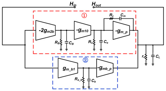
Figure 9.
The LTELDO’s small signal structure using substrate driving technology.
There are two loops in the system, blue and red, as shown in the figure [23]. Among them, the first loop mainly ensures high loop gain so that the output steady-state voltage can be stabilized at the ideal output value, and the second loop mainly ensures a high loop bandwidth so that the power tube can sense that the output load current changes faster and ensure a fast response of the loop. This is because loop 1 cannot guarantee a high bandwidth due to the limitation of static power consumption; in general, the substrate’s transconductance is about 0.25 times the gate-source transconductance , so the loop gain is low under the same conditions, but the tail current can be adjusted to ensure a high loop bandwidth. In the following, the specific expressions of the signal gain, bandwidth, and pole position of the two loops will be detailed, respectively.
3.2.7. The Main Loop
In order to ensure the stability of loop 1, the Miller capacitor Cm is connected to the gate end of the power tube and the output end of the LDO, and the equivalent capacitance of the gate end is increased to separate the main pole and the secondary main pole further, and the secondary main pole is pushed to a higher frequency. However, due to the introduction of a new signal path, a zero in the right-half plane is generated, and the PM drops 90°, which deteriorates the stability. Therefore, it is necessary to add by setting the value of the resistance; the zero in the right-half plane can be transformed into a zero in the left-half plane or can disappear so as to improve the phase margin and ensure the high stability of the loop. The complete results of calculation of the transfer function of loop 1 are
a and b are denoted as follows:
The error amplifier is equivalent to the overall structure’s transconductance, and the transfer function after simplification can be approximately expressed as follows.
c and d are denoted as follows:
From the above transfer function, it can be seen that there are mainly two left half-plane poles in this loop, which are and , respectively. The equivalent impedance of the common-mode feedback resistance point inside the amplifier is small, and the capacitance is very small, so the poles caused by this node are located at a very high frequency and can be ignored in the analysis. The primary pole is located at the output of the amplifier, while the secondary primary pole is located at the output of the LDO, which is expressed as follows.
The specific expression of is as follows:
If the value of is very small, the loop will produce a zero point in the right-half plane, which will deteriorate the loop’s stability. However, when is appropriately chosen, the loop will produce a zero point in the left-half plane , which will improve the phase margin (PM) and ensure loop stability. This loop bandwidth can be approximated as follows.
Following from the expression, of the LDO will increase and the output resistance will increase under small load currents, which will cause the output poles to move to low frequencies, leading to a decrease in the phase margin and the worst loop stability. Figure 10 shows a diagram of the simulated frequency response of loop 2 without an AC signal at 100 μA. The results show that the DC gain of loop 1 is about 67 dB, the bandwidth is 1.6 MHz, and the phase margin after compensating for the Miller capacitor and the zero resistance is about 53°. At this time, the circuit is operating at the minimum load current. Its phase margin is the worst, so the stability of loop 1 under a full load current is guaranteed.
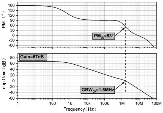
Figure 10.
Frequency response simulation diagram of loop 1 at 100 μA load current.
3.2.8. The Substrate Driving Loop
The transfer function of loop 1 can be expressed as
The loop mainly has two left-half plane poles, and , respectively. Also, because there is no Miller capacitor, the main pole is located at the output end of the LDO, and the other pole is at the output end of the amplifier at the substrate of the power tube. The specific expression is as follows:
The bandwidth of loop 2 can be expressed as follows.
Figure 11 shows the simulation of the frequency response of loop 1 without the AC signal passing through loop 2 under a 100 μA load current. The results show that the DC gain of this amplifier is only 37 dB, but the bandwidth reaches 19 MHz, indicating that the response speed of the loop is fast, which is approximately consistent with the theoretical value.
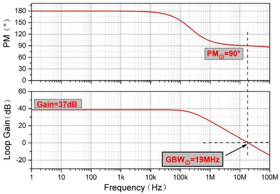
Figure 11.
Frequency response simulation diagram of loop 2 at 100 μA load current.
3.2.9. The Complete System
The total open-loop gain is as follows.
The total open-loop gain is expanded as
It can be seen that the LTE-LDO has a higher gain with an open-loop frequency response at any frequency. In the full load range, the frequency of the main pole in the system is fixed at the output end and will not change with a change in the output load current. The equivalent capacitance of the substrate of the power tube is mainly composed of and and is much smaller than the equivalent capacitance of the gate. Therefore, the secondary main pole of the whole system is located at the output of the main amplifier. Since the substrate amplifier meets the high-bandwidth demand, a large load current is needed, so a < b, and the third pole is . In order to study further, the transfer function is added. Since the two loops share the output load, and and the subsequent power stage circuits can be approximately ignored for convenience of the calculation, and only the independent poles of the two amplifiers are considered to obtain the total system’s function, as shown below:
This can be simplified into
The above expression represents the equivalence of the two loops to a single-pole system, with the zero point generated by multiple loops denoted as , given that it is greater than .
Solving for the zero point generated by the two loops approximately,
The zero point introduced is located at the frequency where the gains of the two amplifiers are equal. This zero point is greater than the frequency of pole , compensating for the phase drop caused by the second pole, thereby improving the phase margin. In order to show the excellent frequency response of the LDO with the substrate driving loop, Figure 12 shows a diagram of the frequency response of an LDO without a substrate driving loop and an LDO with a substrate driving loop in this design. The figure shows that the DC gain is increased from 75 dB to 77 dB, and the bandwidth is increased from 2.5 MHz to 6.9 MHz.
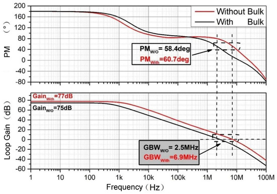
Figure 12.
Frequency response with and without substrate drive at 100 μA load current.
This shows that plays a compensatory role, broadening the loop bandwidth and improving the loop response speed without reducing the phase margin.
3.3. Summary
This section first summarizes the technical structure of traditional fast-transient-response LDOs and then provides an overview of the LTE-LDO. It proceeds with a structural analysis, sequentially introducing the design and implementation of the main error amplifier and the substrate amplifier. Finally, it analyzes the frequency response of the complete structure.
4. Layout Design and Verification
The LDO designed in this paper is based on the SMIC 0.18 μm process. The design and simulation were performed using Cadence IC software. Figure 13 shows the whole layout of the LTE-LDO system, where the bipolar transistor has a large area; R is the local common-mode feedback resistance; C is the Miller capacitor; M-OTA and B-OTA, respectively, represent the error amplifier of the main loop and the error amplifier of the substrate loop; MP represents the power transistor; and the layout’s area is 0.0417 mm2.
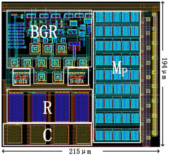
Figure 13.
Substrate -driven LTE-LDO layout.
4.1. LTE-LDO Simulation Verification Results
This section shows the detailed post-simulation results of the overall LTE-LDO circuit, which include the DC, AC, and transient characteristics under the simulation conditions of a standard tt process with a supply voltage of 2.5 V and a temperature of 27 °C.
4.1.1. DC Characteristics
- (1)
- The linear adjustment rate: Figure 14 shows the variation in the output voltage under different load currents when the input voltage changes from 2.5 V to 3.3 V. It can be observed that the best and worst adjustment efficiencies occur under light and heavy load currents, respectively. This is due to the negative correlation between the output resistance and the load current, leading to a low loop gain under light loads and a high loop gain under heavy loads.
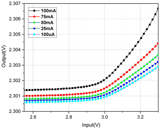 Figure 14. Linear adjustment rate of LTE-LDO at different load currents.
 - (2)
- The load adjustment rate is illustrated in Figure 15, which depicts the output voltage variation under different input voltages as the load current changes linearly from 100 μA to 1 mA. The simulation details the output voltage behavior across input voltages ranging from 2.5 V to 3.3 V in 0.1 V increments.
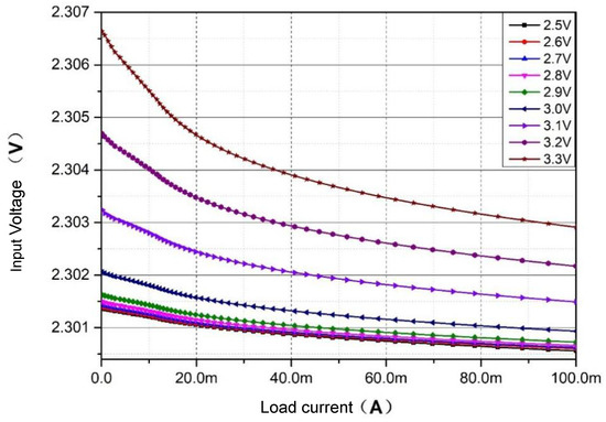 Figure 15. Load adjustment rate of LTE-LDO under different input voltages.
4.1.2. AC Characteristics
Figure 16 shows plots of the frequency response of the LTE-LDO under different load currents. This figure verifies that the fast substrate loop adopted in this paper plays a role in improving the loop bandwidth. In addition, a phase margin above 50° can be achieved in the full-load range, which ensures the fast-transient-response characteristics and loop stability of the LTE-LDO.
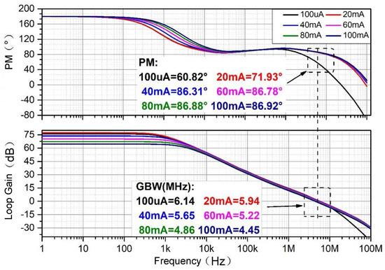
Figure 16.
Frequency response of LTELDO under different load currents.
Figure 17 shows the PSR simulation results at different current loads from 1 Hz to 100 MHz. According to the figure, under load current conditions of 100 μA, 25 mA, 50 mA, 75 mA, and 100 mA, the PSR results at a low frequency are −71.70 dB, −70.01 dB, −67.78 dB, −65.44 dB, and −63.17 dB, respectively, while the noise suppression ability is gradually weakened at a high frequency.
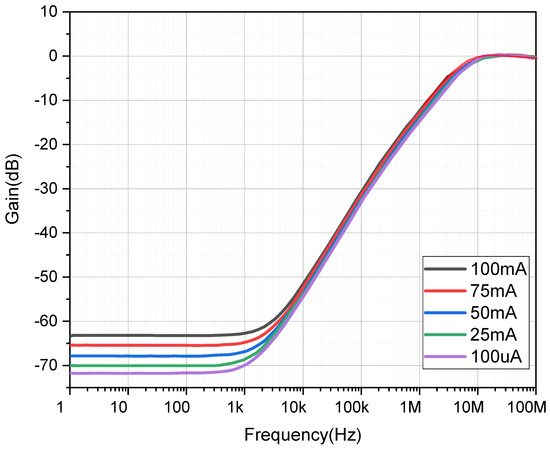
Figure 17.
PSR of LTELDO at different load currents.
4.1.3. Transient Characteristics
To provide a clearer comparison of the transient characteristics with and without the substrate-driven loop, Figure 18 illustrates the output voltage response for both structures during a 100 μA to 100 mA current transition within 100 ns. Under a 2.5 V input, a TT process, and 27 °C, the conventional structure exhibits an undershoot of 188 mV, an overshoot of 195 mV, and a recovery time of 70 ns, while the LTE-LDO achieves an undershoot of 130 mV and an overshoot of 190 mV and stabilizes in 40 ns. The highlighted recovery times of 40 ns versus 70 ns demonstrate a significant improvement in the transient response, which is critical for high-speed signal processing applications where faster stabilization reduces data errors and enhances the signal integrity. In power management systems, this reduction in the recovery time enables more stable voltage regulation during rapid load transients, improving the efficiency and reliability for modern processors and FPGAs that require quick current transitions.
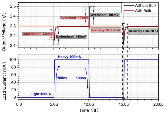
Figure 18.
Transient simulation characteristics with and without substrate drive.
In order to systematically compare the parameter indexes of the proposed LDO with those of previous traditional structures, this section gives a detailed performance comparison, which is shown in the following table. In order to compare the performance more intuitively, a calculation formula is used for the LDO quality factors FoM1 and FoM2.
The proposed LTE-LDO has a strong load capacity by driving a load capacitor of 100 pF and a load current of 100 mA at a static current consumption of only 37 μA, demonstrating its low-power-consumption characteristics. The LTE-LDO shows a greatly improved transient response while consuming a low quiescent current. In addition, the FoM2 value of this structure is the smallest, which verifies that the LTE-LDO can achieve an excellent comprehensive performance.
Through a comparison with all of the literature, it is found that the structure with the substrate loop can improve the trade-off between the power consumption and load current compared with that in the traditional structure without a substrate driver; effectively improve the maximum load current and reduce the loop response time; and significantly enhance the transient characteristics of the traditional structure.
Table 1 shows that the structure proposed in Reference [24] has a lower overshoot and undershoot, but it has a maximum load capacitance of only 50 pF and a maximum load current of just 25 mA. The structure proposed in Reference [25] achieves a static current of only 4 μA, but similarly, its maximum load current is very small, at just 3.1 mA, which cannot meet the requirements of electronic devices demanding large load currents. The structure proposed in Reference [26] demonstrates an improvement in the load current compared to the previous two references, but its line regulation is poor, reaching as high as 37.14 mV/V. The structure proposed in Reference [27] enhances the maximum load current further, but it suffers from a long edge time (500 ns) and poor load regulation (480 μV/mA). The structure proposed in Reference [28] has a limited load current range of only 10 mA and also exhibits poor load regulation at 670 μV/mA. Among these recent structures, none achieve an effective trade-off between the static power consumption and load current. In contrast, the LTE-LDO proposed in this paper effectively addresses this issue, driving a 100 pF load capacitance and a 100 mA load current while consuming only 37 μA of static current, demonstrating a strong load driving capability. The LTE-LDO significantly improves the transient response while maintaining a low static current consumption. Furthermore, the FoM2 value of this structure is the lowest, validating that the LTE-LDO achieves an outstanding comprehensive performance.

Table 1.
Comparison of performance parameters.
5. Conclusions
In this work, a novel design methodology for an on-chip capacitor-less LDO based on substrate technology has been proposed and successfully implemented using the SMIC 0.18 μm CMOS process. Comprehensive post-layout simulations were conducted to validate the design, confirming its feasibility. The proposed LTE-LDO effectively addresses the critical challenges of reducing the static power consumption and improving the load transient response. Through a systematic comparison between AB class and super AB class transconductance amplifiers, it was demonstrated that the super AB class amplifier significantly enhances the slew rate, DC gain, and output current, thereby overcoming the bandwidth limitations of traditional designs.
To optimize the transient performance further, a fast feedback path was integrated at the substrate end, enabling the rapid detection of small-signal disturbances and minimizing the loop response time. This work not only provides a qualitative explanation of the overall circuit’s operation but also presents complete analytical derivation of the transfer function, accounting for the interaction between the substrate loop and the main loop. Finally, a comparative analysis with state-of-the-art LDO designs confirms the superior performance of the proposed work in terms of the low static current consumption and high transient response.
This paper focuses on theoretical analysis and simulation but lacks chip fabrication and comprehensive experimental validation. Future research endeavors should focus on bridging the gap between a theoretical analysis and empirical validation through physical implementation of the LTE-LDO architecture. The fabrication and characterization of an actual chip would provide critical insights into performance discrepancies between the simulation results and measured data, thereby enhancing the scientific rigor of the findings.
Author Contributions
Conceptualization: Y.L. (Yuxin Li); Writing—original draft; writing—review and editing: S.T. Supervision: X.Z. Validation; software: Y.L. (Yanlong Liu). All authors have read and agreed to the published version of the manuscript.
Funding
This research received no external funding.
Data Availability Statement
The original contributions presented in this study are included in the article. Further inquiries can be directed to the corresponding author.
Acknowledgments
The authors would like to thank the laboratory staff for their technical support and assistance during the experiments. We also extend our gratitude to the anonymous reviewers for their valuable comments and suggestions.
Conflicts of Interest
The authors declare no conflicts of interest. The funders had no role in the design of this study; in the collection, analyses, or interpretation of the data; in the writing of the manuscript; or in the decision to publish the results.
References
- Bu, S.; Guo, J.; Leung, K.N. A 200-ps-response-time output-capacitorless low-dropout regulator with unity-gain bandwidth >100 MHz in 130-nm CMOS. IEEE Trans. Power Electron. 2017, 33, 3232–3246. [Google Scholar] [CrossRef]
- Tang, J.; Lee, J.; Roh, J. Low-power fast-transient capacitor-less LDO regulator with high slew-rate class-AB amplifier. IEEE Trans. Circuits Syst. II Express Briefs 2018, 66, 462–466. [Google Scholar] [CrossRef]
- Li, G.; Qian, H.; Guo, J.; Mo, B.; Lu, Y.; Chen, D. DuAl active-feedback frequency compensation for output-capacitorless LDO with transient and stability enhancement in 65-nm CMOS. IEEE Trans. Power Electron. 2019, 35, 415–429. [Google Scholar] [CrossRef]
- Ming, X.; Kuang, J.J.; Liang, H.; Zhang, J.; Qin, Y.; Zhang, Z.W. A fast-transient low-dropout regulator with current-efficient super transconductance cell and dynamic reference control. IEEE Trans. Circuits Syst. I Reg. Pap. 2021, 68, 2354–2367. [Google Scholar] [CrossRef]
- Yu, L.; Yan, J.; Zhao, X.; Dong, L.; Zhong, L.; Liu, Y. A transient-enhanced low-dropout regulator with dynamic current boost technique voltage buffer. AEU-Int. J. Electron. Commun. 2022, 153, 154289. [Google Scholar] [CrossRef]
- Zhao, M.; Zhao, Y.; Zhang, H.; Hu, Y.; Bao, Y.; Ye, L. A 4-μW Bandwidth/Power Scalable Delta–Sigma Modulator Based on Swing-Enhanced Floating Inverter Amplifiers. IEEE J. Solid-State Circuits 2021, 57, 709–718. [Google Scholar] [CrossRef]
- Nagateja, T.; Kumari, N.; Chen, K.H.; Lin, Y.H.; Lin, S.R.; Tsai, T.-Y. A 8-ns Settling Time Fully Integrated LDO with Dynamic Biasing and Bulk Modulation Techniques in 40 nm CMOS. In Proceedings of the 2020 IEEE International Symposium on Circuits and Systems (ISCAS), Seville, Spain, 12–14 October 2020; pp. 1–4. [Google Scholar]
- Ma, G.; Zhan, C.; Zhang, Y. A transient-improved dynamic-replica LDO regulator with bulk modulation. In Proceedings of the 2018 IEEE International Conference on Electron Devices and Solid State Circuits (EDSSC), Shenzhen, China, 6–8 June 2018; pp. 1–2. [Google Scholar]
- Zhang, R.; Liu, Z.; Wang, X. A Capacitor-less LDO with Nested Miller Compensation and Bulk-Driven Techniques in 90 nm CMOS. In Proceedings of the 2021 4th International Conference on Circuits, Systems and Simulation (ICCSS), Kuala Lumpur, Malaysia, 26–28 May 2021; pp. 51–55. [Google Scholar]
- Lv, X.; Zhao, X.; Wang, Y.; Wen, B. An improved non-linear current recycling folded cascode OTA with cascode self-biasing. AEU-Int. J. Electron. Commun. 2019, 101, 182–191. [Google Scholar] [CrossRef]
- Chae, Y.; Han, G. Low voltage, low power, inverter-based switched-capacitor delta-sigma modulator. IEEE J. Solid-State Circuits 2009, 44, 458–472. [Google Scholar] [CrossRef]
- Venkatachala, P.K.; Leuenberger, S.; ElShater, A.; Lee, C.; Xu, Y.; Xiao, B. Process invariant biasing of ring amplifiers using deadzone regulation circuit. In Proceedings of the 2018 IEEE International Symposium on Circuits and Systems (ISCAS), Florence, Italy, 27–30 May 2018; pp. 1–5. [Google Scholar]
- Megawer, K.M.; Hussien, F.A.; Aboudina, M.M.; Mohieldin, A.N. A systematic design methodology for class-AB-style ring amplifiers. IEEE Trans. Circuits Syst. II Express Briefs 2018, 65, 1169–1173. [Google Scholar] [CrossRef]
- Xiao, B.; Venkatachala, P.K.; Xu, Y.; ElShater, A.; Lee, C.Y.; Leuenberger, S. An 80 mA Capacitor-Less LDO with 6.5 µA Quiescent Current and No Frequency Compensation Using Adaptive-Deadzone Ring Amplifier. In Proceedings of the 2019 IEEE Asian Solid-State Circuits Conference (A-SSCC), Macau, Macao, 4–6 November 2019; pp. 39–42. [Google Scholar]
- Guo, Z.; Li, H.; Li, D.; Fan, S.; Gui, X.; Xue, Z. Topological classification-based splitting–combining methodology for analysis of complex multi-loop systems and its application in LDOs. IEEE Trans. Power Electron. 2018, 34, 7025–7039. [Google Scholar] [CrossRef]
- Galan, J.A.; Lopez-Martin, A.J.; Carvajal, R.G.; Ramirez-Angulo, J.; Rubia-Marcos, C. Super class-AB OTAs with adaptive biasing and dynamic output current scaling. IEEE Trans. Circuits Syst. I Reg. Pap. 2007, 54, 449–457. [Google Scholar] [CrossRef]
- Carvajal, R.G.; Ramírez-Angulo, J.; López-Martín, A.J.; Torralba, A.; Galan, J.A.G.; Carlosena, A. The flipped voltage follower: A useful cell for low-voltage low-power circuit design. IEEE Trans. Circuits Syst. I Reg. Pap. 2005, 52, 1276–1291. [Google Scholar] [CrossRef]
- Park, J.E.; Hwang, J.; Oh, J.; Jeong, D.K. 32.4 A 0.4-to-1.2 V 0.0057 mm2 55fs-Transient-FoM Ring-Amplifier-Based Low-Dropout Regulator with Replica-Based PSR Enhancement. In Proceedings of the 2020 IEEE International Solid-State Circuits Conference-(ISSCC), San Francisco, CA, USA, 16–20 February 2020; pp. 492–494. [Google Scholar]
- Kim, S.J.; Chang, S.B.; Seok, M. A High PSRR, low ripple, temperature-compensated, 10-μA-Class Digital LDO Based on current-source power-FETs for a Sub-mW SoC. IEEE Solid-State Circuits Lett. 2021, 4, 88–91. [Google Scholar] [CrossRef]
- Lin, L.; Wang, B.; Rhee, W.; Wang, Z. An Analog-Assisted Digital LDO with 0.37 mV Output Ripple and 5500x Load Current Range in 180 nm CMOS. In Proceedings of the 2022 IEEE International Conference on Integrated Circuits, Technologies and Applications (ICTA), Xi’an, China, 28–30 October 2022; pp. 106–107. [Google Scholar]
- Tan, X.L.; Koay, K.C.; Chong, S.S.; Chan, P.K. A FVF LDO Regulator with DuAl-Summed Miller Frequency Compensation for Wide Load Capacitance Range Applications. IEEE Trans. Circuits Syst. I Reg. Pap. 2014, 61, 1304–1312. [Google Scholar] [CrossRef]
- Wang, Y.; Shu, Z.; Zhang, Q.; Zhao, X.; Chen, S.; Tang, F. A Low-Voltage and Power-Efficient Capless LDO Based on the Biaxially Driven Power Transistor Technique for Respiration Monitoring System. IEEE Trans. Biomed. Circuits Syst. 2022, 16, 1153–1165. [Google Scholar] [CrossRef] [PubMed]
- Hong, S.W.; Cho, G.H. High-gain wide-bandwidth capacitor-less low-dropout regulator (LDO) for mobile applications utilizing frequency response of multiple feedback loops. IEEE Trans. Circuits Syst. I Reg. Pap. 2016, 63, 46–57. [Google Scholar] [CrossRef]
- Huang, S.; Li, Y.; Mo, B.; Guo, J.; Chen, D. An Output-Capacitorless Adaptively Biased Low-Dropout Regulator with Maximum 132-MHz UGF and Without Minimum Loading Requirement. In Proceedings of the 2018 31st IEEE International System-on-Chip Conference (SOCC), Arlington, VA, USA, 4–7 September 2018; pp. 206–212. [Google Scholar]
- Wang, Z.; Mirabbasi, S. A 0.58-to-0.9-V Input 0.53-V Output 2.4-μW Current-Feedback Low-Dropout Regulator With 99.8% Current Efficiency. IEEE Solid-State Circuits Lett. 2019, 3, 1–4. [Google Scholar] [CrossRef]
- Xin, Y. Research and Design of High Efficiency Low Pressure Difference Linear Regulator for MEMS Seismometer. Master’s Thesis, China University of Geosciences, Beijing, China, 2021. [Google Scholar]
- Li, S.; Zhao, X.; Dong, L.; Yu, L.; Wang, Y. Design of a capacitor-less adaptively biased low dropout regulator using recycling folded cascode amplifier. AEU-Int. J. Electron. Commun. 2021, 135, 153745. [Google Scholar] [CrossRef]
- Han, X.; Ki, W.H.; Wu, L.; Gao, Y. Ultrahigh PSR Output-Capacitor-Free Adaptively Biased 2-Power-Transistor LDO With 200-mV Dropout. IEEE Solid-State Circuits Lett. 2022, 5, 106–109. [Google Scholar] [CrossRef]
- Bhattacharjee, I.; Chowdary, G. A 0.45 mV/V Line Regulation, 0.6 V Output Voltage, Reference-Integrated, Error Amplifier-Less LDO With a 5-Transistor Regulation Core. IEEE J. Solid-State Circuits 2023, 58, 3231–3241. [Google Scholar] [CrossRef]
- Kim, T.; Kim, B.; Roh, J. A 54-nA Quiescent Current Capless LDO With 39-dB PSRR at 1 MHz Using a Load-Tracking Bandwidth Extension Technique. IEEE Trans. Circuits Syst. II Express Briefs 2024, 71, 1556–1560. [Google Scholar] [CrossRef]
Disclaimer/Publisher’s Note: The statements, opinions and data contained in all publications are solely those of the individual author(s) and contributor(s) and not of MDPI and/or the editor(s). MDPI and/or the editor(s) disclaim responsibility for any injury to people or property resulting from any ideas, methods, instructions or products referred to in the content. |
© 2025 by the authors. Licensee MDPI, Basel, Switzerland. This article is an open access article distributed under the terms and conditions of the Creative Commons Attribution (CC BY) license (https://creativecommons.org/licenses/by/4.0/).