Article

Thermal Management of Wide-Bandgap Power Semiconductors: Strategies and Challenges in SiC and GaN Power Devices

1
Department of Electrical Engineering, Soongsil University, Seoul 06978, Republic of Korea
2
School of Electronic Engineering, Soongsil University, Seoul 06978, Republic of Korea
*
Author to whom correspondence should be addressed.
Electronics 2025, 14(21), 4193; https://doi.org/10.3390/electronics14214193
Submission received: 10 September 2025 / Revised: 13 October 2025 / Accepted: 13 October 2025 / Published: 27 October 2025
(This article belongs to the Topic Wide Bandgap Semiconductor Electronics and Devices)

Abstract

Wide-Bandgap (WBG) semiconductors—silicon carbide (SiC) and gallium nitride (GaN)— enable high-power-density conversion, but performance is limited by where heat is generated and how it is removed. This review links device-level loss mechanisms (conduction and switching, including output-capacitance hysteresis and dynamic on-resistance) to structure-driven hot spots within the ultra-thin (tens of nanometers) two-dimensional electron gas (2DEG) channel of GaN HEMTs and to thermal boundary resistance at layer interfaces. We compare wire-bondless package concepts—double-sided cooling, embedded packaging, and interleaved planar layouts—and survey system-level cooling that shortens the conduction path and raises heat-transfer coefficients. The impact on reliability is discussed using temperature-sensitive electrical parameters (e.g., on-state VDS, threshold voltage, drain leakage, di/dt, and gate current) for real-time junction-temperature estimation and compact electro-thermal RC models for remaining-useful-life prediction. Evidence from recent literature points to interface resistance in GaN-on-SiC as a primary bottleneck, while near-junction cooling and advanced packages are effective mitigations. We argue for integrated co-design—devices, packaging, electromagnetic interference (EMI)-aware layout, and cooling—together with interface engineering and health monitoring to deliver reliable, high-density WBG systems.

1. Introduction

The efficient operation of power semiconductor devices in modern power conversion systems is closely linked to global energy efficiency. However, current silicon (Si)-based devices exhibit limitations at high voltage, high temperature, and high frequency, necessitating complex and costly cooling systems. To address these challenges, Wide-Bandgap (WBG) semiconductors, including silicon carbide (SiC) and gallium nitride (GaN), have emerged as materials that enable high-voltage, high-temperature, and high-speed switching owing to their Wide-Bandgap, nearly tenfold higher critical electric field, and superior thermal conductivity [1,2]. SiC offers rapid switching because of its low drift-layer resistance and the absence of minority-carrier storage. Moreover, SiC bipolar devices, particularly those with thin blocking layers, show improved characteristics relative to Si devices. GaN high electron mobility transistors (HEMTs) provide high power density and efficiency at high frequency, enabling miniaturization and easing cooling requirements. Accordingly, WBG semiconductors are positioned to overcome key constraints of Si technologies in electric vehicles, aerospace, and renewable energy [2,3]. Despite these advantages, critical thermal bottlenecks remain. In particular, localized self-heating and the limited maturity of high-temperature packaging present significant hurdles. For example, although SiC has high thermal conductivity, it still requires advanced heat dissipation at the package level, whereas GaN faces challenges in thermal dissipation and reliability due to its lower thermal conductivity and heterojunction architecture [1,2]. Furthermore, defects introduced during SiC crystal growth and degradation in bipolar devices significantly impede reliability, while GaN can suffer performance degradation due to elevated field stress, intrinsic crystalline defects, and long-term stability issues associated with high dislocation density [1,3]. While numerous excellent reviews have addressed specific aspects of WBG thermal management—such as advanced packaging architectures or novel cooling solutions—a significant research gap remains in providing a holistic, multi-scale perspective that links device-level physics with system-level reliability. For example, challenges at the nanometer scale, including thermal boundary resistance (TBR) across AlGaN/GaN heterointerfaces only tens of nanometers thick, are often treated in isolation from macro-scale packaging and cooling decisions. Moreover, reliability concerns, such as long-term degradation under mission profiles, are seldom integrated into these discussions. This review addresses these shortcomings by systematically connecting the fundamental heat-generation mechanisms in WBG devices with packaging, cooling, and reliability strategies required for robust system-level thermal design.

2. Thermal Generation in SiC and GaN Power Devices

2.1. Fundamental Thermal Properties and Loss Mechanisms

The performance and reliability of power semiconductor devices are fundamentally influenced by intrinsic thermal properties and the loss mechanisms that occur during operation. SiC and GaN can operate under high-voltage and high-temperature conditions thanks to their Wide-Bandgaps (2.9–3.4 eV) and critical electric field strengths (2.2–4 MV cm−1), outperforming conventional Si in these regimes [2,3,4,5]. These characteristics make them highly suitable for applications requiring high power density and high-efficiency power conversion. SiC exhibits high thermal conductivity (3.3–4.9 W cm−1 K−1; approximately 330–490 W m−1 K−1), enabling superior heat removal. GaN’s thermal conductivity decreases with temperature [2,6]. In GaN-based structures, TBR at the substrate interface becomes a significant thermal bottleneck; aluminum nitride (AlN) buffer layers and interfacial defects increase TBR, and acoustic-phonon scattering exacerbates this at elevated temperatures [7,8].

2.1.1. Conduction Losses

Conduction losses scale approximately with I 2 R DS ( on ) ; R DS ( on ) itself increases with temperature (and can vary with bias). SiC mitigates conduction losses through its low drift-layer resistance, whereas GaN benefits from high electron mobility. Nevertheless, under specific operating conditions, GaN conduction losses can rise markedly, and for both device types, R DS ( on ) tends to decrease at lower temperatures [9,10].

2.1.2. Switching Losses

Switching losses occur during the transient overlap of voltage and current; higher switching speeds in WBG devices can markedly reduce these losses. GaN typically exhibits lower switching losses than SiC due to lower gate and drain charge and higher carrier mobility. For example, GaN current-aperture vertical electron transistors (CAVETs) have demonstrated approximately twice the switching speed and about one-third the switching loss of SiC metal-oxide-semiconductor field-effect transistors (MOSFETs) [10]. In addition, SiC devices are not affected by minority-carrier storage, facilitating rapid switching and further loss reduction as temperature decreases [1,11].

2.1.3. Other Switching-Related Phenomena

Other switching-related phenomena also contribute to energy dissipation. Reverse-recovery loss is negligible for GaN HEMTs (no minority-carrier body diode), whereas in SiC MOSFETs it is lower than in Si MOSFETs but not negligible. By contrast, losses associated with output capacitance ( C OSS ), gate charge, and voltage overshoot from parasitic inductance are often more significant [4,12,13]. In GaN devices, dynamic degradation—observed as an increase in R DS ( on ) during switching—may occur due to trapping effects, and its severity can escalate at higher operating frequencies. Reported measurements indicate that dynamic R D S ( o n ) increases monotonically from several hundred kHz up to approximately 2 MHz under hard-switching stress, after which the effect tends to saturate as the switching period becomes shorter than the trapping/detrapping time constants. The magnitude of degradation strongly depends on test conditions: higher off-state drain bias and longer stress duration exacerbate trapping, hard-switching produces significantly larger resistance increases than soft-switching, and large drain current or low duty cycle further intensifies the effect. Accurate characterization of these losses remains challenging, since measurements must capture both high off-state voltages and millivolt-level on-state resistance within wide dynamic ranges, and conventional double-pulse test methods often underestimate steady-state degradation. These factors make loss separation and quantification in GaN and SiC devices highly non-trivial [14,15].

2.2. Device Structure and Localized Heating

Effective thermal management in power semiconductor devices is fundamental to ensuring both performance and reliability. In particular, device structure directly affects localized heat intensification and hotspot formation. Devices utilizing SiC and GaN as WBG materials offer high efficiency and high-voltage capability; however, heat generation can concentrate in specific regions, limiting maximum power density and reducing lifetime [1]. Heat-generation pathways differ across device types. SiC MOSFETs comprise resistive components—including the channel, junction field-effect transistor (JFET) region, and drift layer—that act as primary heat sources. Of these, channel and JFET resistances dominate at lower voltage ratings, whereas the drift layer becomes the main contributor at higher voltages (above 3 kV ) [2]. In contrast, GaN HEMTs conduct current through a two-dimensional electron gas (2DEG) formed within the AlGaN/GaN heterostructure, focusing conduction losses into an ultrathin channel and thereby intensifying localized heating [1,3,16,17]. The structural characteristics of GaN HEMTs introduce several unique thermal challenges. They are prone to hotspots in the gate-drain region, where high electric fields lead to hot-electron effects, trap generation, and the reverse piezoelectric effect, degrading performance and reliability [18,19,20] (Figure 1). Electroluminescence (EL) imaging confirms this, showing localized emission in field-crowding regions consistent with trap formation and current reduction [21]. Furthermore, because native GaN substrates are scarce, GaN HEMTs are typically grown on foreign substrates (Si, SiC, or sapphire). This heteroepitaxy yields high TBR at the interface, which raises channel temperature and complicates operation at high power densities [16]. Even cascode GaN devices—which stack a GaN HEMT and a Si MOSFET to reduce parasitics—introduce a complex thermal path that can elevate junction temperature and must be managed carefully [22,23].
Consequently, accurate temperature-field mapping and structure-aware thermal analysis are essential for devising effective cooling strategies and ensuring reliability, as localized hotspots degrade performance and can trigger failure [18,24].

3. Thermal Management Solutions for WBG Power Devices: Advanced Packaging and Cooling Techniques

3.1. Thermal Pathways and Packaging Materials

Maximizing WBG device performance and reliability requires efficient thermal pathways and high-reliability packaging materials. Conventional wire bonding is often unsuitable for WBG devices, which switch rapidly [25,26,27]. For substrates, SiC (in GaN-on-SiC) offers a significant thermal advantage, exhibiting high thermal conductivity of 3.3–4.9  W cm 1 K 1 (approximately 330–490  W m 1 K 1 ). GaN-on-Diamond can further reduce channel temperature owing to the diamond substrate’s thermal conductivity exceeding 700 W m 1 K 1 , thereby enhancing both performance and lifetime [1,2,28,29]. Because native GaN substrates remain limited, GaN is predominantly grown heteroepitaxially on Si, sapphire, or SiC, which can introduce heat-transfer bottlenecks [3,19]. Die-attach and top-side interconnection technologies are critical to thermal robustness and reliability under high-temperature operation. Traditional Sn-based solders are constrained by relatively low melting points and intermetallic compound (IMC) formation [30], motivating high-reliability alternatives [31]. IMC growth is often accelerated by microstructural defects at the solder interface (e.g., grain boundaries, oxides, interfacial roughness), which act as heterogeneous nucleation sites; in addition, unbalanced Cu/Sn interdiffusion can induce Kirkendall voiding, degrading thermo-mechanical integrity over life [30,32]. Silver-sintered joints provide excellent electrical/thermal conductivity and high-temperature stability but face electromigration (EM) and cost challenges [2,30,31,32,33,34,35]. Copper-sintered joints offer comparable performance with improved EM resistance, though oxidation control and process windows remain nontrivial [1,2,3,31,36,37,38]. As another approach, transient liquid phase (TLP) bonding achieves stable IMCs after low-temperature bonding, improving high-temperature reliability [3,30]. TBR is a significant component of the overall thermal resistance in GaN-on-SiC, where AlN nucleation and defect layers elevate interface resistance. To mitigate TBR, surface-activated bonding (SAB) has emerged as a promising interface technology, enabling high-quality interfaces and thermal boundary conductance (TBC) values approaching 230 MW m 2 K 1  [1,2,39]. In summary, meeting the high-power-density demands of WBG devices requires a materials-and-interfaces-centric strategy: select high-conductivity substrates, minimize TBR, and deploy die-attach and top-side interconnections with proven high-temperature stability. Paired with the advanced package architectures detailed in Section 3.2, this approach is instrumental in elevating WBG system effectiveness [3,30].

3.2. Advanced Package Architectures

Conventional wire bonding, originally developed for Si devices, is a bottleneck that limits the attainable switching speed and power density of WBG packages. The constraints arise from three factors: substantial parasitic inductance, restricted vertical heat removal, and reduced reliability under thermomechanical stress—all of which degrade performance and lifetime [25,26,27,40]. To address these limitations, wire-bondless top-side interconnections have gained traction. Representative solutions include copper fins, ribbons, clips, thin films, and Cu-sintered paste interconnects, which together reduce parasitic elements and improve heat spreading [19,20,21]. In parallel, silver and copper microparticle sintering and transient liquid-phase bonding are recognized as reliable assembly approaches that combine excellent electrical/thermal conductivity with high-temperature stability [2,3,30] (Figure 2).

3.2.1. Double-Sided Cooling (DSC)

DSC enhances heat removal by extracting heat from both top and bottom surfaces, thereby lowering thermal resistance and equalizing temperature distribution. Copper-clip structures reduce thermal resistance by approximately 20% [27] versus single-sided layouts, while flip-chip bonding further mitigates parasitic inductance. The use of thermally conductive adhesive films (TCAFs) reduces interfacial thermal resistance. DSC has been widely implemented in SiC MOSFET high-power modules and is considered essential for extending device lifetime under high thermal loads [26,41,42,43,44].

3.2.2. Embedded Packaging

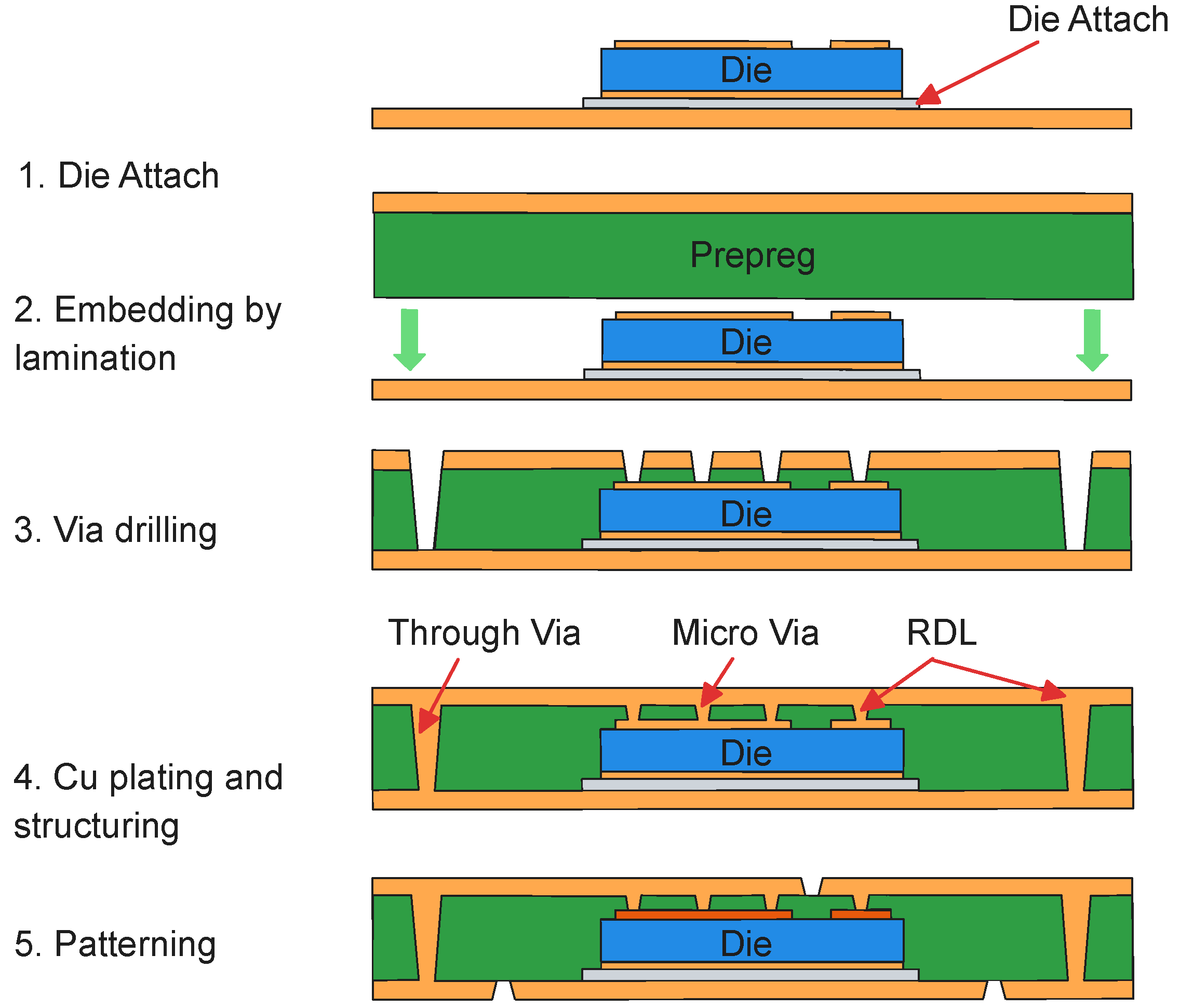
Embedded packaging places power dies inside the printed circuit board (PCB), which lowers parasitic inductance/capacitance, reduces package height, and creates an efficient vertical thermal path. In SiC MOSFET modules, this approach has cut parasitic inductance by up to 87.6%, down to 1.24 nH  [27]. When combined with substrate-embedded microchannels for localized convective cooling, the junction temperature can drop by approximately 50 °C, enabling more than 22% [27] higher saturation current due to improved thermal uniformity. The embedded paradigm also provides inherent electromagnetic interference (EMI) shielding and significantly improves robustness against thermal cycling and electrical overstress [29,45,46,47,48,49]. The typical process flow is illustrated in Figure 3.

3.2.3. Interleaved Planar Packaging

Interleaved planar packaging addresses die-to-die thermal and electrical coupling in parallel-connected WBG modules. The Interleaved Switch Unit (ISU) architecture achieves a 57% [40] reduction in thermal coupling resistance via vertical (z-axis) thermal separation, improving thermal decoupling. In addition, the Current Commutator Structure (CCS) balances current distribution and reduces loop inductance to 3.8 nH  [40], thereby improving transient performance and current sharing. Experiments at elevated temperature show a 20 °C [40] lower junction temperature relative to conventional planar packaging, while maintaining current imbalance within 6% [40]. Overall, interleaved planar packaging provides a robust, electromagnetically optimized, and scalable integration path for next-generation high-density WBG modules (Figure 4).

3.3. System-Level Cooling Techniques

The high-temperature, high-voltage, and high-frequency operating characteristics of WBG devices increase power density and heat flux, underscoring the need for advanced system-level thermal management. Among WBG materials, GaN poses greater thermal-management challenges than SiC due to its relatively low thermal conductivity [1,2,29]. Conventional approaches face inherent limits in high-density WBG systems. Air cooling, while simple and cost-effective, lacks the heat-transfer capacity to manage the intense heat flux generated by WBG devices. Although SiC-based converters can maintain thermal stability with fan-assisted heat sinks, effectiveness is limited under high-power or thermally stressed conditions [26]. Indirect liquid cooling via cold plates offers moderate improvement; however, the extended thermal path between heat sources and coolant yields a thermal resistance of 0.3–0.4  K cm 2 W 1 , which is often above the approximately 0.2 K cm 2 W 1 target needed for compact, high-performance WBG applications [1,26,29]. To overcome these limitations, advanced techniques pursue two goals: shorten the thermal conduction path and maximize the heat transfer coefficient (HTC). Direct liquid cooling improves heat removal by bringing coolant into direct contact with the chip or substrate surface, thereby reducing TBR and increasing heat-transfer efficiency [29,50,51]. Jet impingement cooling uses high-speed jets from micro-nozzles to target hotspots, achieving high HTC; it is effective for thermally demanding devices such as GaN monolithic microwave integrated circuit (MMIC) power amplifiers [29,52,53,54]. Phase-change cooling leverages latent heat (e.g., heat pipes) for rapid heat removal. Microchannel cooling routes coolant through tens to hundreds of μ m channels etched in or beneath the substrate; embedded microchannels further shorten the conduction path and have demonstrated up to a 43% [29] reduction in thermal resistance while mitigating self-heating and thermal coupling in dense power modules [55,56,57,58]. In summary, direct liquid cooling, jet impingement, phase-change, and embedded microchannel cooling are key options that extend beyond conventional solutions and enable compact, efficient, and thermally robust architectures for next-generation WBG power conversion [29,50,51,52,53,54,55,56,57,58].
To provide a clear comparative perspective, Table 1 consolidates the key performance improvements, practical advantages, and trade-offs of representative packaging and cooling techniques discussed in this section.

4. Reliability Issues and Thermal Modeling

4.1. Overview of Reliability Issues and Assessment Methodologies

While the advantages of WBG semiconductors such as SiC and GaN are well established, ensuring their long-term reliability and accurately forecasting their operational lifespan remain critical challenges [1,2,59]. Reliability concerns in SiC primarily stem from various crystallographic and point defects, whose propagation can be accelerated by thermo-mechanical stress. Extended defects such as micropipes, basal plane dislocations (BPDs), and stacking faults increase leakage current and reduce breakdown voltage [60,61,62], while deep-level point defects (such as the Z1/2 and EH6/7 centers) act as carrier recombination centers that shorten carrier lifetime [2]. Fundamentally, understanding the link between such structural defects and the resulting electronic and thermal properties often relies on atomistic modeling approaches like Density Functional Theory (DFT) [63]. Furthermore, degradation of bonding materials and metal electromigration at elevated temperatures undermines long-term stability [19,64]. The reliability of GaN HEMTs is affected by several degradation mechanisms rooted in their heteroepitaxial structure. Hot-carrier effects, for instance, can generate new charge trapping centers, such as interface traps at the AlGaN/GaN interface or point defects (e.g., vacancies) within the GaN buffer, leading to phenomena like current collapse and increased gate-leakage current [19]. In particular, transconductance degradation and gate lag are observed under “semi-ON” operating conditions, and the EL technique enables real-time evaluation of hot-carrier distributions [19,64]. Accelerated life testing (ALT) is critical for analyzing degradation and failure mechanisms. High-temperature gate bias (HTGB), high-temperature reverse bias (HTRB), power cycling (PC), and thermal cycling (TC) efficiently identify vulnerable failure modes within short durations and facilitate parameterization of lifetime-prediction models [64,65]. While well-established industrial standards from the Joint Electron Device Engineering Council (JEDEC)—such as JESD22 (thermal and electrical stress tests) and JESD47 (qualification procedures)—and from the Automotive Electronics Council (AEC), including AEC-Q100 and AEC-Q101 for automotive ICs and discrete devices, provide a crucial framework for reliability assessment, their direct application to WBG devices remains limited. These standards, which rely on stress tests such as HTGB, HTRB, TC, and temperature–humidity bias (THB), were originally designed for Si technologies and do not fully capture WBG-specific degradation mechanisms such as dynamic R DS ( on ) shifts or TBR-induced hotspots. Moreover, the elevated operating temperatures of SiC and GaN may activate new failure modes with high activation energies that are absent in conventional Si operation, making lifetime extrapolation from Si standards potentially misleading. Consequently, the development of WBG-specific qualification methodologies is an active area of focus for industry bodies, including the JEDEC JC-70 committee [66]. Thermal management is directly linked to device reliability. Thermal stress accounts for approximately 60% of primary failure causes [67], and accurate estimation of junction temperature ( T j ) is essential for reliable lifetime prediction. Analytical methods such as coupled electro-thermal analysis, lumped thermal models (LTM), and the finite element method (FEM) are used to predict T j and identify hotspots [64,68,69,70]. Temperature-sensitive electrical parameters (TSEPs) are widely used for real-time thermal monitoring and early fault detection. Representative TSEPs include V DS ( on ) , threshold voltage ( V th ), drain leakage current ( I dss ), d I / d t , and gate current ( I gp ); these parameters reflect accumulated thermal stress and form the basis of condition-based maintenance strategies [64,71]. They are also leveraged in active thermal-control implementations. Taken together, an integrated approach—combining reliability-mechanism analysis, ALT, thermal modeling, and real-time monitoring—is essential to ensure the long-term operational capability and safety of WBG devices.

4.2. Health Monitoring and Lifetime Prediction Techniques

In SiC- and GaN-based power systems that demand high reliability, health-monitoring-based thermal and electrical diagnostics are essential for proactive fault identification and lifetime estimation. Conventional manual inspections are limited, especially under high switching density and elevated temperatures, motivating the development of active health monitoring technologies [64,65]. TSEPs serve as key diagnostic metrics: they indicate cumulative thermal stress and enable real-time estimation of junction temperature ( T j ). Representative TSEPs include V DS ( on ) , V th , I dss , Miller plateau voltage, d I / d t , and I gp , which can also signal potential failure or package degradation [64,71,72,73,74]. These real-time, metric-driven prediction approaches fall into two broad categories. Physics-of-failure (PoF) models rely on the underlying mechanisms of specific failure modes—such as thermal fatigue, adhesive degradation, and oxide deterioration—and often employ cumulative damage laws (e.g., Miner’s rule). Data-driven methods use empirical TSEP streams and operational histories to improve lifetime-prediction accuracy, leveraging machine learning, dynamic Bayesian networks (DBN), and dynamic reliability block diagrams (DRBD) [65,75]. Recently, for remaining useful life (RUL) estimation from time-series data, failure-correlation models have been used to track degradation and its relationship to environmental stressors such as high temperature, humidity, and mechanical vibration. Notably, multi-stress interactions are significant in WBG devices, making reliability difficult to predict with single-variable models [64]. Furthermore, recent advanced models have begun to address the non-uniform temperature distributions and localized hotspots that are particularly severe in WBG devices. Traditional lifetime models that rely on average junction temperature can lead to inaccurate RUL predictions. To overcome this, new methodologies explicitly incorporate on-chip temperature distributions. For example, Wu et al. proposed a wire-bond degradation model that accounts for the different temperature swings experienced by individual bond wires, enabling more precise RUL estimation by modeling the progressive failure of multiple wires rather than only the first one [76]. Incorporating spatial thermal gradients in this manner represents a significant step toward more realistic and physically accurate lifetime prediction. In summary, as high-speed switching and high-density designs become commonplace, passive thermal management and static design alone are insufficient. A comprehensive health-monitoring framework—combining real-time sensing, precursor detection, and lifetime prediction—is a prerequisite for broader industrial adoption of SiC and GaN devices.

4.3. Thermal-Aware Design for Extended Lifetime

Building on the reliability assessment and monitoring techniques discussed above, a thermal-aware design philosophy integrates these elements to proactively ensure long-term device reliability. WBG devices experience elevated thermal stress due to high switching frequencies and power densities, which gradually degrades bonding wires, solder interfaces, and gate oxides through repeated power cycling [64,65]. Accordingly, ALT—including HTGB, HTRB, and PC—is applied to forecast and address underlying damage mechanisms, with PoF models often using Miner’s rule for life prediction [64,65]. At the system level, DRBDs and DBNs capture temporal dependencies and interconnections for reliability assessment [65]. TSEPs enable real-time state monitoring. Key examples include V DS ( on ) , V th , I dss , Miller plateau voltage, and I gp . Notably, for SiC MOSFETs the low temperature dependence of R DS ( on ) and its higher sensitivity to gate-source voltage ( V g s ) warrant care in interpretation [64]. Optimizing the thermal-resistance path is critical for reliability improvement. Dimensions of solder-mask openings, selection of high-conductivity die-attach materials, and the strategic arrangement of vias together reduce junction-to-die, die-to-sink, and junction-to-ambient thermal resistances. For example, increasing the via count from 4 to 25 reduced the peak temperature of the power amplifier by approximately 52% (from 492.956 °C to 234.836 °C) [77]. In electro-thermal simulations, FEM-derived compact RC electro-thermal network models predict T j dynamics and support RUL assessment [68,69,78]. These models, often structured as Cauer or Foster networks, derive their thermal resistance ( R t h ) and capacitance ( C t h ) parameters by fitting the network’s response to transient thermal data. This data is typically generated either from detailed Finite Element Method (FEM) simulations or, as demonstrated by Xu et al., from experimental thermal impedance measurements and datasheet curves [68]. Beyond lifetime estimation, these models integrate naturally with thermal-path optimization and control-oriented dynamic thermal management. In summary, a comprehensive thermal-aware design strategy—combining PoF-based lifetime models, TSEP-based temperature estimation, thermal-path optimization, and integrated modeling—is essential for early detection of failure mechanisms and for ensuring the reliability of thermally sensitive WBG devices [79].

5. Technology Integration and Patent Trends

5.1. Co-Design and Integration Strategies

SiC- and GaN-based WBG power semiconductors offer a Wide-Bandgap, high critical electric field, and excellent thermal conductivity, enabling high efficiency, high power density, and operation at elevated temperatures. Realizing these device-level advantages at the system level, however, requires a multidisciplinary co-design approach that jointly considers device physics, packaging, circuit topologies, gate drivers, EMI filters, and cooling—beyond optimizing isolated components [10,11,12,27,80,81]. High switching speed enables higher power density and smaller passives, but it also introduces voltage overshoot, increased EMI, switching losses, and thermal stress. These fast-transient behaviors couple through parasitic inductance and layout, and dynamic changes in R DS ( on ) can trigger thermal runaway. Accordingly, simultaneous optimization of electrical performance, thermal behavior, and mechanical integrity is essential [10,11,12,27,82]. From a reliability perspective, WBG devices exhibit failure modes distinct from Si. In SiC, BPDs and threading edge dislocations (TEDs) shorten carrier lifetime and raise leakage current [2], while gate-oxide traps and V th instability are additional concerns [2,64]. Elevated current density accelerates electromigration, worsening solder-layer degradation and self-heating variability [64]. GaN devices involve a complex interplay of self-heating, current collapse, and hot-carrier degradation [3,12,19,83]. Under “semi-ON” conditions, transconductance degradation driven by hot carriers is often observed, and at higher drain-source voltage V DS (approximately 30–50  V ), the reverse piezoelectric effect and AlGaN barrier breakdown can increase gate leakage [19]. To address these mechanisms within a unified framework, temperature-sensing and condition monitoring must be integrated into the co-design loop. TSEP-based monitoring can separate the temperatures of the internal HEMT and the Si MOSFET in cascode GaN via reverse-current analysis [23], while d I / d t and I gp are commonly used in SiC MOSFETs [64,71]. These diagnostics improve observability but introduce cost and complexity that must be balanced at the system level [64]. Packaging and layout co-optimization further reduces the coupling between fast transients, thermal hotspots, and EMI. DSC, embedded packaging, and interleaved planar structures mitigate current imbalance across parallel dies and reduce parasitics [10,40,45,82]. Cu-based interconnections (Cu clips, Cu sintering, etc.) can cut loop inductance from 14 nH to 2.37 nH versus wire bonding, thereby lowering EMI and switching losses [25,27]. Cu sintering is effective at high temperature, though conductivity degradation and residual-stress sensitivity remain process-dependent [84]. Finally, substrate and interface engineering is essential to limit TBR while sustaining electrical performance. GaN-on-Diamond offers exceptional thermal conductivity, but a high TBR can be performance-limiting, motivating measures such as via-hole insertion [7,8,83]. In parallel, optimizing GaN layer thickness helps redistribute heat flux and relieve hotspots; three-dimensional (3D) simulations indicate that doping-layer thickness strongly affects temperature beneath the gate [7,28,29]. In sum, industrial realization of SiC and GaN demands system-level co-design that closes the loop among devices, interconnects, layout/EMI control, and cooling, with shared targets (power density, EMI compliance, Δ T j , and lifetime). Such an integrated strategy is foundational for the next phase of technological progress.

5.2. Patent-Based Analysis of Integration Trends in WBG Power Semiconductors

To examine how the co-design strategies outlined in Section 5.1 translate into practice, this section analyzes patent trends in WBG power electronics and highlights representative families that catalyzed electro-thermal co-optimization.
  • Methodology. We queried WIPS ON (accessed on 4 September 2025, KST) for patent families filed in 2010–2025, focusing on Wide-Bandgap (SiC and GaN) power devices with relevance to packaging and thermal integration. To avoid pulling Si-only results, we applied the following Boolean query (English keywords; Korean synonyms were also checked in the same portal): (Listing 1)
Listing 1. Boolean query used for patent search in WIPS ON database.
(SiC OR GaN OR “Wide-Bandgap” OR WBG OR “power semiconductor”)
AND (“thermal management” OR cooling OR “heat dissipation” OR “heat sink”
OR “thermal interface material” OR TIM OR packaging
OR “thermal resistance” OR “thermal conductivity”)
Results were deduplicated by INPADOC family; counts were assigned to the earliest priority year; geography reflects the first-priority country; and assignee names were harmonized. Representative families were then selected using the following three objective filters: (i) claim-level relevance, i.e., independent claims disclose packaging/thermal integration elements (die-attach/TIM, wire-bondless interconnects, near-junction cooling, or electro-thermal co-design); (ii) impact, measured by age-normalized forward citations (top-quartile within the cohort); and (iii) breadth/status, i.e., coverage in ≥2 jurisdictions or one major office (US/EP/JP/CN) with at least one granted member. As a tie-breaker, assignee significance was considered when families were otherwise comparable. Illumination-only LED families were excluded unless the claims disclose packaging/thermal constructs transferable to power-device applications.
  • Representative Families. SiC—US 8,329,252 B2 [85] exemplifies epitaxial/process innovations that suppress defect formation and improve substrate/epi quality, directly supporting the reliability targets in Section 4.1 and the thermal strategies in Section 3. GaN—US 2011/0297914 A1 [86] describes a wire-bond-free flip-chip stack that shortens the vertical heat path and reduces parasitics. Although originally framed for LEDs, this packaging architecture is platform-neutral and is cited here as an early integration precedent, consistent with Section 2.2 and Section 3.2.
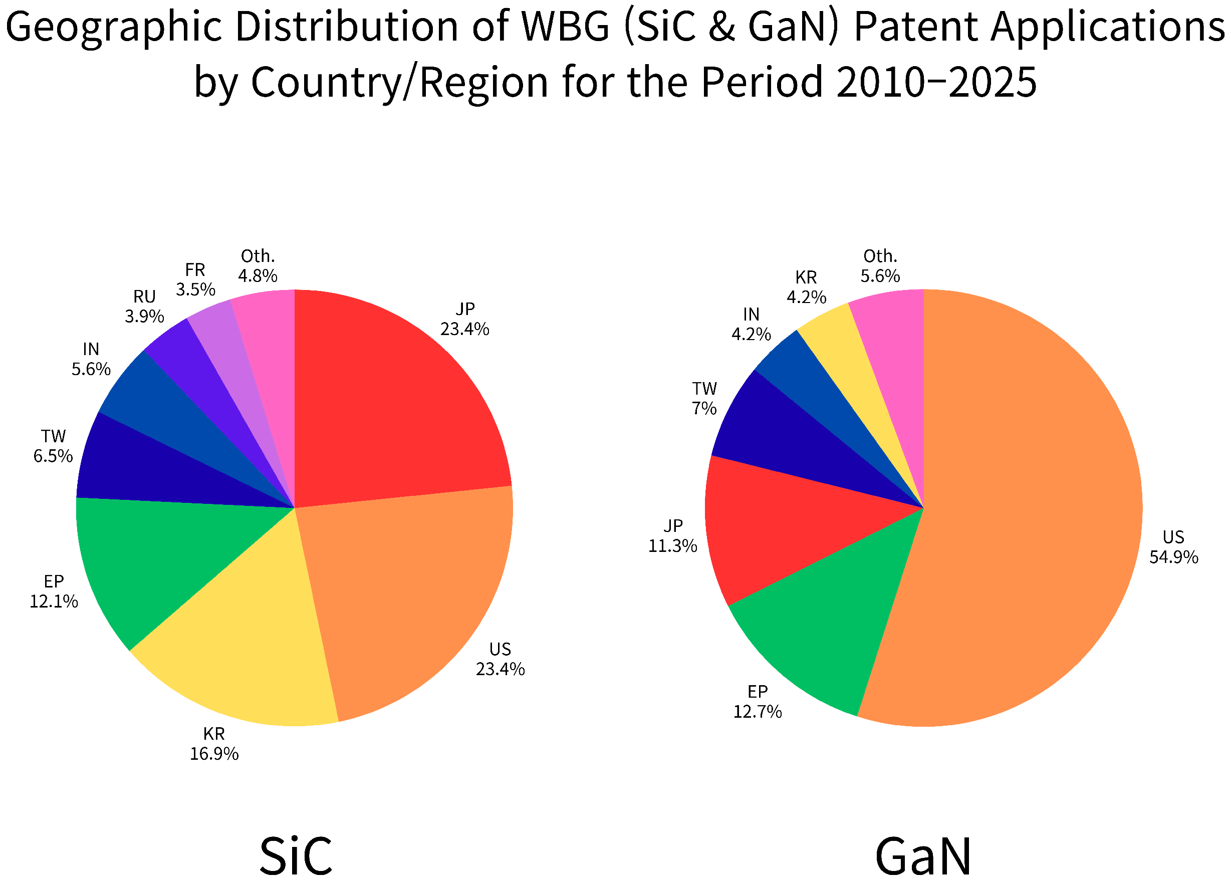
  • Trends and Implications. These examples reflect a broader evolution from quantitative expansion to qualitative, integration-centric innovation (Figure 5). Geographically, the United States and Japan lead in SiC, while the U.S. holds a commanding share in GaN (Figure 6). Overall, securing intellectual property (IP) on high-quality substrates, advanced interconnects, and electro-thermal co-design has become decisive for delivering reliable, high-density WBG systems at scale.
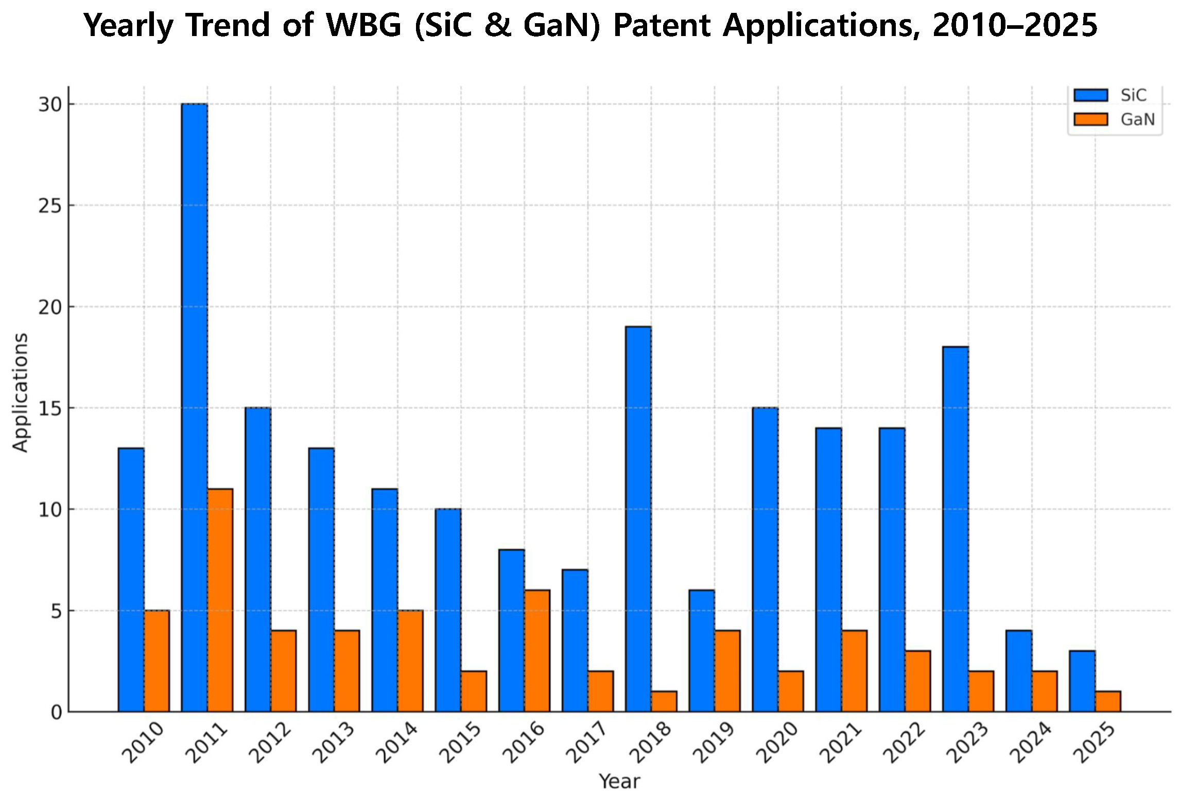
Figure 5. Yearly trend of WBG (SiC and GaN) patent families, 2010–2025. Counts aggregated by earliest priority year; INPADOC family deduplication; Source: WIPS ON (accessed on 4 September 2025, KST). Due to publication lags, the trend is directional.
Electronics 14 04193 g005
Figure 6. Geographic distribution of WBG (SiC and GaN) patent families by first-priority country, 2010–2025. INPADOC family deduplication; Source: WIPS ON (accessed on 4 September 2025, KST).
Electronics 14 04193 g006
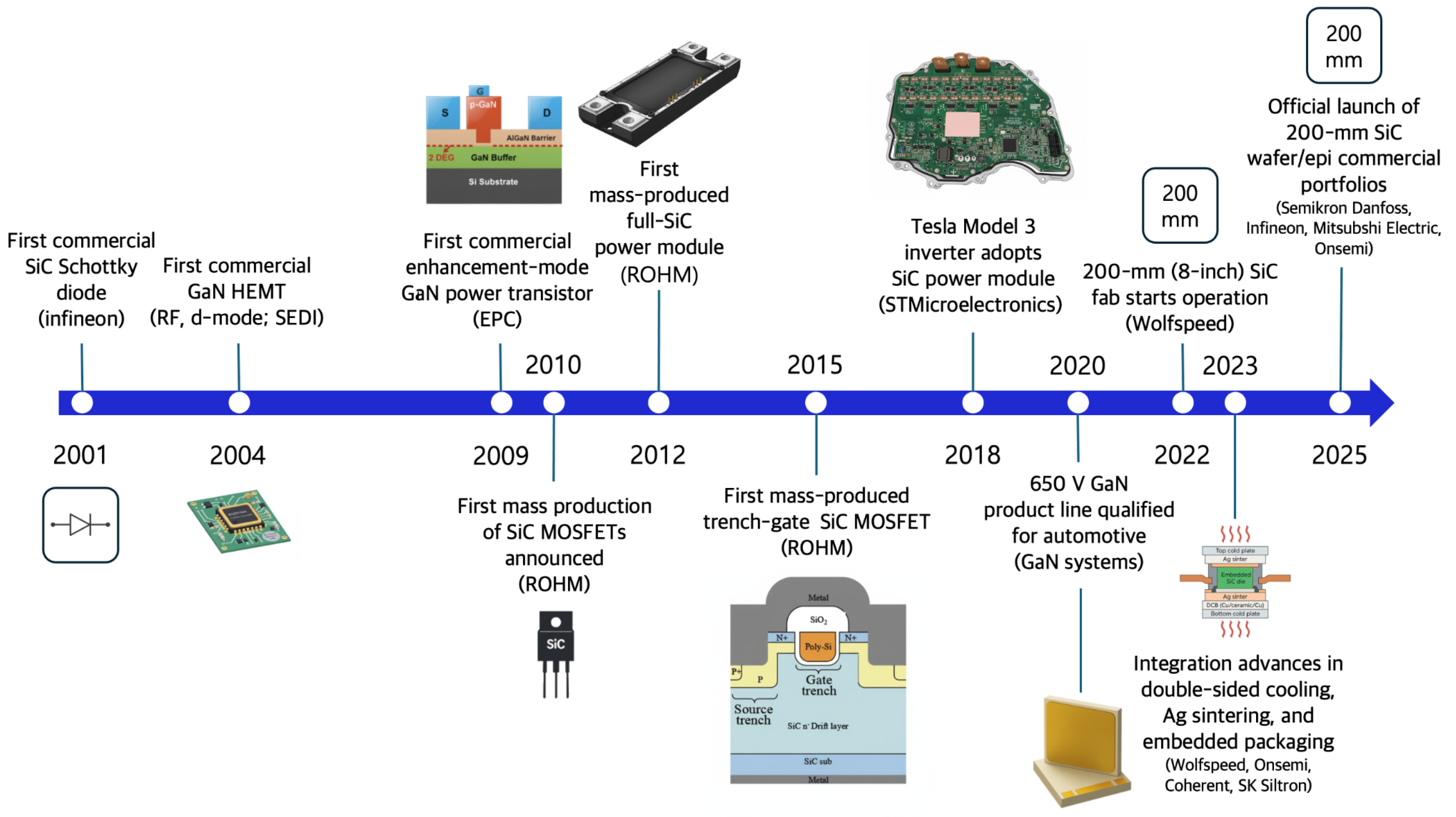
To complement the statistical patent analysis (Figure 5 and Figure 6), Figure 7 provides a chronological view of major packaging and cooling innovations, highlighting how technological milestones from 2010 to 2025 align with the trends discussed in this section. As a synthesis of the literature in Section 3 and Section 5.2, it consolidates major milestones without introducing new data.

6. Conclusions

In modern power conversion, SiC- and GaN-based WBG devices promise unprecedented power density, yet this potential is fundamentally capped by localized self-heating. This review has shown that the root of the problem lies at the multi-scale interface: from hotspots in the ultrathin 2DEG channels and TBR in GaN-on-SiC to the parasitic elements in conventional packaging. While advanced solutions such as double-sided cooling, embedded packaging, and near-junction microchannels offer effective mitigations, they must be coupled with real-time health monitoring via TSEPs and robust lifetime models. The evidence overwhelmingly demonstrates that isolated, component-level optimizations are insufficient. Therefore, an integrated co-design—spanning devices, packaging, EMI-aware layout, and cooling—is the only viable strategy to overcome these interconnected challenges and deliver reliable, high-density WBG systems.
Looking forward, this co-design principle must extend to next-generation architectures. Standardizing processes and reliability for 3D heterogeneous integration will be critical, particularly in managing new failure modes such as thermal crosstalk between stacked dies and stress-induced delamination at material interfaces. Furthermore, the development of physics-informed, AI-driven active thermal management, guided by digital-twin frameworks, will be essential to close the loop from design to real-time operational reliability, ultimately enabling reliable, high-density WBG power systems.

Author Contributions

Conceptualization, G.H.; methodology, G.H. and S.P.; software, G.H. and J.K.; validation, J.K. and S.P.; formal analysis, S.P.; investigation, G.H., J.K. and S.P.; resources, G.H.; data curation, G.H.; writing—original draft preparation, G.H.; writing—review and editing, J.K.; visualization, J.K. and S.P.; supervision, W.B.; project administration, G.H. All authors have read and agreed to the published version of the manuscript.

Funding

This research received no external funding.

Data Availability Statement

The original contributions presented in this study are included in the article. Further inquiries can be directed to the corresponding author.

Acknowledgments

During the preparation of this manuscript, the authors used ChatGPT (GPT-4 version, OpenAI) for language translation and minor wording edits. The authors reviewed and edited the text and take full responsibility for the content.

Conflicts of Interest

The authors declare no conflicts of interest.

Abbreviations

The following abbreviations and symbols are used in this manuscript:
Abbreviations
2DEGTwo-Dimensional Electron Gas
3DThree-Dimensional
AECAutomotive Electronics Council
AEC-Q100AEC Qualification Standard for Integrated Circuits
AEC-Q101AEC Qualification Standard for Discrete Semiconductors
ALTAccelerated Life Testing
AlNAluminum Nitride
BPDBasal Plane Dislocation
CAVETCurrent-Aperture Vertical Electron Transistor
CCSCurrent Commutator Structure
DBNDynamic Bayesian Network
DFTDensity Functional Theory
DRBDDynamic Reliability Block Diagram
DSCDouble-Sided Cooling
ELElectroluminescence
EMElectromigration
EMIElectromagnetic Interference
FEMFinite Element Method
GaNGallium Nitride
HEMTHigh Electron Mobility Transistor
HTCHeat Transfer Coefficient
HTGBHigh-Temperature Gate Bias
HTRBHigh-Temperature Reverse Bias
IMCIntermetallic Compound
IPIntellectual Property
ISUInterleaved Switch Unit
JEDECJoint Electron Device Engineering Council
JESD22JEDEC Standard JESD22: Stress-Test Procedures
JESD47JEDEC Standard JESD47: Reliability Qualification of Integrated Circuits
JFETJunction Field-Effect Transistor
LTMLumped Thermal Model
MMICMonolithic Microwave Integrated Circuit
MOSFETMetal-Oxide-Semiconductor Field-Effect Transistor
PCPower Cycling
PCBPrinted Circuit Board
PoFPhysics-of-Failure
RCResistance–Capacitance (network)
RULRemaining Useful Life
SABSurface-Activated Bonding
SiSilicon
SiCSilicon Carbide
TCThermal Cycling
TBCThermal Boundary Conductance
TBRThermal Boundary Resistance
TCAFThermally Conductive Adhesive Film
TDBTime-Dependent Breakdown
TEDThreading Edge Dislocation
THBTemperature–Humidity Bias
TLPTransient Liquid Phase
TSEPTemperature-Sensitive Electrical Parameter
WBGWide-Bandgap
Parameters and Symbols
C OSS Output Capacitance
d I / d t Current Slew Rate
I dss Drain Leakage Current
I gp Gate Current
R DS ( on ) On-State Resistance
T j Junction Temperature
Δ T j Junction Temperature Variation
V DS Drain–Source Voltage
V g s Gate–Source Voltage
V th Threshold Voltage
V DS ( on ) On-State Drain–Source Voltage
R t h Thermal Resistance (Compact Network Parameter)
C t h Thermal Capacitance (Compact Network Parameter)
Z t h ( t ) Transient Thermal Impedance
Z j c Junction-to-Case Thermal Impedance

References

  1. Millan, J.; Godignon, P.; Perpina, X.; Perez-Tomas, A.; Rebollo, J. A Survey of Wide Bandgap Power Semiconductor Devices. IEEE Trans. Power Electron. 2014, 29, 2155–2163. [Google Scholar] [CrossRef]
  2. Kimoto, T. Material Science and Device Physics in SiC Technology for High-Voltage Power Devices. Jpn. J. Appl. Phys. 2015, 54, 040103. [Google Scholar] [CrossRef]
  3. Mishra, U.K.; Parikh, P.; Wu, Y.F. AlGaN/GaN HEMTs—An Overview of Device Operation and Applications. Proc. IEEE 2002, 90, 1022–1031. [Google Scholar] [CrossRef]
  4. Priyadarshini, S.; Sridutt, L.; Prakash, S.; Gunasekaran, K.; Samikannu, R. Thermal Modelling and Efficiency Analysis of On-Board Charger Using Wide-Gap Semiconductor Devices for EV Application. In Proceedings of the 2024 3rd Odisha International Conference on Electrical Power Engineering, Communication and Computing Technology (ODICON), Bhubaneswar, India, 8–9 November 2024; pp. 1–6. [Google Scholar]
  5. Buffolo, M.; Favero, D.; Marcuzzi, A.; De Santi, C.; Meneghesso, G.; Zanoni, E.; Meneghini, M. Review and Outlook on GaN and SiC Power Devices: Industrial State-of-the-Art, Applications, and Perspectives. IEEE Trans. Electron Devices 2024, 71, 1344–1355. [Google Scholar] [CrossRef]
  6. Zheng, Q.; Li, C.; Rai, A.; Leach, J.H.; Broido, D.A.; Cahill, D.G. Thermal Conductivity of GaN, AlN, and SiC from 150 K to 850 K. Phys. Rev. Mater. 2019, 3, 014601. [Google Scholar] [CrossRef]
  7. Mitterhuber, L.; Kosednar-Legenstein, B.; Vohra, A.; Borga, M.; Posthuma, N.; Kraker, E. Correlation of Heat Transport Mechanism and Structural Properties of GaN High Electron Mobility Transistors. J. Appl. Phys. 2024, 136, 245102. [Google Scholar] [CrossRef]
  8. Wang, K.; Hu, W.; Wu, S.; Wang, H.; Padhiar, M.A.; Ji, Y. Simulation Investigation of Effects of Substrate and Thermal Boundary Resistance on Performances of AlGaN/GaN HEMTs. Phys. Scr. 2024, 99, 065554. [Google Scholar] [CrossRef]
  9. Abd El-Azeem, S.M.; El-Ghanam, S.M. Comparative Study of Gallium Nitride and Silicon Carbide MOSFETs as Power Switching Applications under Cryogenic Conditions. Cryogenics 2020, 107, 103071. [Google Scholar] [CrossRef]
  10. Emon, A.I.; Carlton, H.; Harris, J.; Krone, A.; Mirza, A.; Hassan, M.; Yuan, Z.; Huitink, D.; Luo, F. Design and Optimization of 650 V/60 A Double-Sided Cooled Multichip GaN Module. In Proceedings of the 2021 IEEE Applied Power Electronics Conference and Exposition (APEC), Phoenix, AZ, USA, 14–17 June 2021; pp. 2313–2317. [Google Scholar]
  11. Agrawal, B. Loss Minimization Using Linear Soft-Switching with Wide Bandgap Devices in Efficient High-Frequency DC-DC Converters. Master’s Thesis, McMaster University, Hamilton, ON, Canada, 2017. [Google Scholar]
  12. Jafari, A.; Nikoo, M.S.; Perera, N.; Yildirim, H.K.; Karakaya, F.; Soleimanzadeh, R.; Matioli, E. Comparison of Wide-Band-Gap Technologies for Soft-Switching Losses at High Frequencies. IEEE Trans. Power Electron. 2020, 35, 12595–12600. [Google Scholar] [CrossRef]
  13. Emon, A.I.; Mustafeez-ul-Hassan; Mirza, A.B.; Kaplun, J.; Vala, S.S.; Luo, F. A Review of High-Speed GaN Power Modules: State of the Art, Challenges, and Solutions. IEEE J. Emerg. Sel. Top. Power Electron. 2023, 11, 2707–2729. [Google Scholar] [CrossRef]
  14. Matioli, E.; Zhu, H.; Perera, N.; Nikoo, M.S.; Jafari, A.; van Erp, R. Switching Losses in Power Devices: From Dynamic on Resistance to Output Capacitance Hysteresis. In Proceedings of the 2023 25th European Conference on Power Electronics and Applications (EPE’23 ECCE Europe), Aalborg, Denmark, 4–8 September 2023; pp. 1–7. [Google Scholar]
  15. Gill, L.; DasGupta, S.; Neely, J.C.; Kaplar, R.J.; Michaels, A.J. A Review of GaN HEMT Dynamic On-Resistance and Dynamic Stress Effects on Field Distribution. IEEE Trans. Power Electron. 2024, 39, 517–537. [Google Scholar] [CrossRef]
  16. Ramyar, A.; Lou, Y.; Avestruz, A.T. Accurate Temperature Measurement of Active Area for Wide-Bandgap Power Semiconductors. In Proceedings of the 2023 IEEE 24th Workshop on Control and Modeling for Power Electronics (COMPEL), Ann Arbor, MI, USA, 25–28 June 2023; pp. 1–8. [Google Scholar]
  17. Gaska, R.; Osinsky, A.; Yang, J.W.; Shur, M.S. Self-Heating in High-Power AlGaN-GaN HFETs. IEEE Electron Device Lett. 1998, 19, 89–91. [Google Scholar] [CrossRef]
  18. Bhatti, H.I.; Yuvaraja, S.; Wang, C.; Tang, X.; Li, X. Monolithic Integrated Micro-Thin-Film Thermocouples for On-Chip Temperature Measurement of GaN HEMTs. IEEE Trans. Electron Devices 2024, 71, 7734–7739. [Google Scholar] [CrossRef]
  19. Meneghesso, G.; Verzellesi, G.; Danesin, F.; Rampazzo, F.; Zanon, F.; Tazzoli, A.; Meneghini, M.; Zanoni, E. Reliability of GaN High-Electron-Mobility Transistors: State of the Art and Perspectives. IEEE Trans. Device Mater. Reliab. 2008, 8, 332–343. [Google Scholar] [CrossRef]
  20. Wang, X.D.; Hu, W.D.; Chen, X.S.; Lu, W. The Study of Self-Heating and Hot-Electron Effects for AlGaN/GaN Double-Channel HEMTs. IEEE Trans. Electron Devices. 2012, 59, 1393–1401. [Google Scholar] [CrossRef]
  21. Sarua, A.; Ji, H.; Kuball, M.; Uren, M.J.; Martin, T.; Hilton, K.P.; Balmer, R.S. Integrated Micro-Raman/Infrared Thermography Probe for Monitoring of Self-Heating in AlGaN/GaN Transistor Structures. IEEE Trans. Electron Devices 2006, 53, 2438–2447. [Google Scholar] [CrossRef]
  22. Rahman, M.; Hasan, A.S.M.K.; Mantooth, H.A.; Song, X. High Temperature Characterization and Degradation Test of a Cascode Gallium Nitride Field Effect Transistor. In Proceedings of the 2024 IEEE 11th Workshop on Wide Bandgap Power Devices & Applications (WiPDA), Dayton, OH, USA, 4–6 November 2024; pp. 1–6. [Google Scholar] [CrossRef]
  23. Wu, L.; Deng, E.; Wang, Y.; Xu, S.; Hua, W.; Yang, S.; Ding, L. A Multi-Currents Method for Junction Temperature Separation of Cascode GaN. IEEE Trans. Power Electron. 2024, 39, 15567–15575. [Google Scholar] [CrossRef]
  24. Won, Y.; Cho, J.; Agonafer, D.; Asheghi, M.; Goodson, K.E. Cooling Limits for GaN HEMT Technology. In Proceedings of the 2013 IEEE Compound Semiconductor Integrated Circuit Symposium (CSICS), Monterey, CA, USA, 13–16 October 2013; pp. 1–5. [Google Scholar]
  25. Ain, K.N.; Zhang, G.Q.; Rodrigues, A.; Hasan, M.N.; Holzmann, D.; Geens, K.; Chatterjee, U.; Roshanghias, A. An Introduction to Wire-Bondless Discrete GaN Power Packages with Top-Side Cu Sinterconnects. In Proceedings of the 2024 IEEE 10th Electronics System-Integration Technology Conference (ESTC), Berlin, Germany, 11–13 September 2024; pp. 1–5. [Google Scholar]
  26. Lee, H.; Smet, V.; Tummala, R. A Review of SiC Power Module Packaging Technologies: Challenges, Advances, and Emerging Issues. IEEE J. Emerg. Sel. Top. Power Electron. 2020, 8, 239–255. [Google Scholar] [CrossRef]
  27. Wang, L.; Wang, W.; Hueting, R.J.E.; Rietveld, G.; Ferreira, J.A. Review of Topside Interconnections for Wide Bandgap Power Semiconductor Packaging. IEEE Trans. Power Electron. 2023, 38, 472–490. [Google Scholar] [CrossRef]
  28. Faqir, M.; Manoi, A.; Mrotzek, T.; Knippscheer, S.; Massiot, M.; Buchta, M.; Blanck, H.; Rochette, S.; Vendier, O.; Kuball, M. New GaN Power-Electronics Packaging Solutions: A Thermal Analysis Using Raman Thermography. J. Microelectron. Electron. Packag. 2011, 8, 110–113. [Google Scholar] [CrossRef]
  29. Lu, D.; Ye, Y.; Liu, R.; Wu, M.; Du, X.; Yu, L.; Qiao, J.; Liu, Z.; Kong, Y.; Jiao, B. Near-Junction Thermal Management of GaN-on-SiC MMIC Power Amplifier Through Substrate Embedded Microchannel. IEEE Trans. Electron Devices 2024, 71, 502–509. [Google Scholar] [CrossRef]
  30. Hou, F.; Sun, Z.; Su, M.; Fan, J.; You, X.; Li, J.; Wang, Q.; Cao, L.; Zhang, G. Review of Die-Attach Materials for SiC High-Temperature Packaging. IEEE Trans. Power Electron. 2024, 39, 13471–13486. [Google Scholar] [CrossRef]
  31. Kim, D.; Nagao, S.; Chen, C.; Wakasugi, N.; Yamamoto, Y.; Suetake, A.; Takemasa, T.; Sugahara, T.; Suganuma, K. Online Thermal Resistance and Reliability Characteristic Monitoring of Power Modules with Ag Sinter Joining and Pb, Pb-Free Solders During Power Cycling Test by SiC TEG Chip. IEEE Trans. Power Electron. 2021, 36, 4977–4990. [Google Scholar] [CrossRef]
  32. Chen, G.; Han, D.; Mei, Y.H.; Cao, X.; Wang, T.; Chen, X.; Lu, G.Q. Transient Thermal Performance of IGBT Power Modules Attached by Low-Temperature Sintered Nanosilver. IEEE Trans. Device Mater. Reliab. 2012, 12, 124–132. [Google Scholar] [CrossRef]
  33. Bai, J.G.; Yin, J.; Zhang, Z.; Lu, G.Q.; van Wyk, J.D. High-Temperature Operation of SiC Power Devices by Low-Temperature Sintered Silver Die-Attachment. IEEE Trans. Adv. Packag. 2007, 30, 506–510. [Google Scholar] [CrossRef]
  34. Wang, M.; Mei, Y.H.; Jin, J.; Chen, S.; Li, X.; Lu, G.Q. Pressureless Sintered-Silver Die-Attach at 180 °C for Power Electronics Packaging. IEEE Trans. Power Electron. 2021, 36, 12141–12145. [Google Scholar] [CrossRef]
  35. Knoerr, M.; Kraft, S.; Schletz, A. Reliability Assessment of Sintered Nano-Silver Die Attachment for Power Semiconductors. In Proceedings of the 2010 12th Electronics Packaging Technology Conference, Singapore, 8–10 December 2010; pp. 56–61. [Google Scholar]
  36. Saccon, R.; Bhogaraju, S.K.; Elger, G. Cu Sintering for High Power Electronics Packaging—Challenges and Solutions. In Proceedings of the GMM-Fachbericht 105: Mikro-Nano-Integration, Aachen, Germany, 21 November 2022; pp. 26–31. [Google Scholar]
  37. Liu, X.; Zhou, Q.; Zhao, X.; Koh, S.W.; Ye, H.; Zhang, G. Study and Application of Nano Cu Sintering Technology in Power Electronics Packaging. In Proceedings of the 2021 IEEE 71st Electronic Components and Technology Conference (ECTC), San Diego, CA, USA, 1 June–4 July 2021; pp. 1928–1932. [Google Scholar]
  38. Duch, S.; Gunst, S.; Reh, S. The Attractions, Challenges, and Potential of Copper Sinter Paste for Power Electronics Applications. In Proceedings of the 13th International Conference on Integrated Power Electronics Systems (CIPS 2024), Düsseldorf, Germany, 12–14 March 2024; p. 6. [Google Scholar]
  39. Mu, F.; Cheng, Z.; Shi, J.; Shin, S.; Xu, B.; Shiomi, J.; Graham, S.; Suga, T. High Thermal Boundary Conductance across Bonded Heterogeneous GaN—SiC Interfaces. ACS Appl. Mater. Interfaces 2019, 11, 33428–33434. [Google Scholar] [CrossRef]
  40. Yang, F.; Lixin, J.; Wang, L.; Zhang, F.; Wang, B.; Zhao, C.; Wang, J.; Bayer, C.; Ferreira, J. Interleaved Planar Packaging Method of Multichip SiC Power Module for Thermal and Electrical Performance Improvement. IEEE Trans. Power Electron. 2022, 37, 1615–1629. [Google Scholar] [CrossRef]
  41. Tang, G.; Wai, L.C.; Lim, S.B.; Ye, Y.L.; Lau, B.L.; Yamamoto, K.; Zhang, X. Development of a Novel Lead Frame Based Double Side Liquid Cooling High Performance SiC Power Module. In Proceedings of the 2021 IEEE 71st Electronic Components and Technology Conference (ECTC), San Diego, CA, USA, 1 June–4 July 2021; pp. 118–124. [Google Scholar]
  42. Li, B.; Yang, X.; Wang, K.; Zhu, H.; Wang, L.; Chen, W. A Compact Double-Sided Cooling 650 V/30 A GaN Power Module with Low Parasitic Parameters. IEEE Trans. Power Electron. 2022, 37, 426–439. [Google Scholar] [CrossRef]
  43. Zhu, M.; Wang, L.; Pei, Y.; Yang, F.; Cheng, Z.; Gao, K. Compact Spatially Symmetric Double-Sided Embedded Packaging Method for Parallel SiC MOSFETs. In Proceedings of the 2024 25th International Conference on Electronic Packaging Technology (ICEPT), Tianjin, China, 7–9 August 2024; pp. 1–4. [Google Scholar]
  44. Tian, X.; Jia, N.; DeVoto, D.; Paret, P.; Bai, H.; Tolbert, L.M.; Cui, H. PCB-on-DBC GaN Power Module Design with High-Density Integration and Double-Sided Cooling. IEEE Trans. Power Electron. 2024, 39, 507–516. [Google Scholar] [CrossRef]
  45. Nakamura, K.; Shigematsu, K.; Imaoka, J.; Yamamoto, M. Prototyping and Evaluation of SiC Half Bridge Circuit Using Power Device Embedded Module Process Towards Future Three Dimensional Packaging. In Proceedings of the 2023 IEEE CPMT Symposium Japan (ICSJ), Kyoto, Japan, 15–17 November 2023; pp. 196–199. [Google Scholar]
  46. Risch, R.; Biela, D.J. PCB-Embedded Packaging for Ultra-Fast Switching of SiC MOSFETs. In Proceedings of the 12th International Conference on Integrated Power Electronics Systems (CIPS 2022), Berlin, Germany, 15–17 March 2022; pp. 269–275. [Google Scholar]
  47. Wang, J.; Liu, Z.; Peng, H.; Ren, X. A Novel Intelligent Power Module in Embedded Packaging with Low Parasitic Inductance and Low Thermal Resistance. In Proceedings of the 2024 25th International Conference on Electronic Packaging Technology (ICEPT), Tianjin, China, 7–9 August 2024; pp. 1–4. [Google Scholar]
  48. Tian, X.; Jia, N.; Chertkovsky, D.B.; Sun, J.; Bai, H.; Tolbert, L.M.; Cui, H. An Embedded GaN Power Module with Double-Sided Cooling and High-Density Integration. In Proceedings of the 2022 IEEE Energy Conversion Congress and Exposition (ECCE), Detroit, MI, USA, 9–13 October 2022; pp. 1–7. [Google Scholar]
  49. Zhang, C.; Liu, X.; Li, J.; Song, G.; Ye, H. Simulation Study on Thermal Mechanical Properties of Different Embedded Packaging Structures and Materials of GaN Devices. In Proceedings of the 2020 21st International Conference on Electronic Packaging Technology (ICEPT), Guangzhou, China, 1–5 August 2020; pp. 1–5. [Google Scholar]
  50. McPherson, B.; McGee, B.; Simco, D.; Olejniczak, K.; Passmore, B. Direct Liquid Cooling of High Performance SiC Power Modules. In Proceedings of the 2017 IEEE International Workshop on Integrated Power Packaging (IWIPP), Delft, The Netherlands, 5–7 April 2017. [Google Scholar]
  51. Morozumi, A.; Hokazono, H.; Nishimura, Y.; Ikeda, Y.; Nabetani, Y.; Takahashi, Y. Direct Liquid Cooling Module with High Reliability Solder Joining Technology for Automotive Applications. In Proceedings of the 2013 25th International Symposium on Power Semiconductor Devices & ICs (ISPSD), Kanazawa, Japan, 26–30 May 2013; pp. 435–438. [Google Scholar]
  52. Gould, K.; Cai, S.Q.; Neft, C.; Bhunia, A. Liquid Jet Impingement Cooling of a SiC Power Conversion Module for Vehicle Applications. IEEE Trans. Power Electron. 2015, 30, 2975–2984. [Google Scholar] [CrossRef]
  53. Barua, H.; Chowdhury, S.; Wilkins, J.; Ozpineci, B. Single and Double-Sided Jet Impingement Cooling for SiC-Based Power Modules. In Proceedings of the 2023 IEEE 10th Workshop on Wide Bandgap Power Devices & Applications (WiPDA), Charlotte, NC, USA, 4–6 December 2023; pp. 74–79. [Google Scholar]
  54. Mouawad, B.; Skuriat, R.; Li, J.; Johnson, C.M.; DiMarino, C. Development of a Highly Integrated 10 kV SiC MOSFET Power Module with a Direct Jet Impingement Cooling System. In Proceedings of the 2018 IEEE 30th International Symposium on Power Semiconductor Devices and ICs (ISPSD), Chicago, IL, USA, 13–17 May 2018; pp. 256–259. [Google Scholar]
  55. Jung, K.W.; Kharangate, C.R.; Lee, H.; Palko, J.; Zhou, F.; Asheghi, M.; Dede, E.M.; Goodson, K.E. Microchannel Cooling Strategies for High Heat Flux (1 kW/cm2) Power Electronic Applications. In Proceedings of the 2017 16th IEEE Intersociety Conference on Thermal and Thermomechanical Phenomena in Electronic Systems (ITherm), Orlando, FL, USA, 30 May–2 June 2017; pp. 98–104. [Google Scholar]
  56. van Erp, R.; Kampitsis, G.; Nela, L.; Ardebili, R.S.; Matioli, E. Embedded Microchannel Cooling for High Power-Density GaN-on-Si Power Integrated Circuits. In Proceedings of the 2020 19th IEEE Intersociety Conference on Thermal and Thermomechanical Phenomena in Electronic Systems (ITherm), Orlando, FL, USA, 21–23 July 2020; pp. 53–59. [Google Scholar]
  57. Chen, X.; Donmezer, F.N.; Kumar, S.; Graham, S. A Numerical Study on Comparing the Active and Passive Cooling of AlGaN/GaN HEMTs. IEEE Trans. Electron Devices 2014, 61, 4056–4061. [Google Scholar] [CrossRef]
  58. van Erp, R.; Kampitsis, G.; Matioli, E. Efficient Microchannel Cooling of Multiple Power Devices with Compact Flow Distribution for High Power-Density Converters. IEEE Trans. Power Electron. 2020, 35, 7235–7245. [Google Scholar] [CrossRef]
  59. Ni, Z.; Lyu, X.; Yadav, O.P.; Cao, D. Review of SiC MOSFET-Based Three-Phase Inverter Lifetime Prediction. In Proceedings of the 2017 IEEE Applied Power Electronics Conference and Exposition (APEC), Tampa, FL, USA, 26–30 March 2017; pp. 1007–1014. [Google Scholar]
  60. Li, X.; Deng, X.; Liao, Z.; Li, X.; Jia, R.; Zhang, B. Failure Mechanism of 1200-V SiC MOSFET with Embedded Schottky Barrier Diode Under Short-Circuit Condition. IEEE Trans. Electron. Devices 2025, 72, 1259–1263. [Google Scholar] [CrossRef]
  61. Schrock, J.A.; Ray II, W.B.; Lawson, K.; Bilbao, A.; Bayne, S.B.; Holt, S.L.; Cheng, L.; Palmour, J.W.; Scozzie, C. High-Mobility Stable 1200-V, 150-A 4H-SiC DMOSFET Long-Term Reliability Analysis Under High Current Density Transient Conditions. IEEE Trans. Power Electron. 2015, 30, 2891–2895. [Google Scholar] [CrossRef]
  62. Yang, X.; Liu, J.; Wang, B.; Zhang, G. Pulsed Overcurrent Capability of Power Semiconductor Devices in Solid-State Circuit Breakers: SiC MOSFET vs. Si IGBT. In Proceedings of the 2022 IEEE Applied Power Electronics Conference and Exposition (APEC), Houston, TX, USA, 20–24 March 2022; pp. 966–973. [Google Scholar]
  63. Pela, R.R.; Hsiao, C.L.; Hultman, L.; Birch, J.; Gueorguiev, G.K. Electronic and optical properties of core–shell InAlN nanorods: A comparative study via LDA, LDA-1/2, mBJ, HSE06, G0W0 and BSE methods. Phys. Chem. Chem. Phys. 2024, 26, 7504–7514. [Google Scholar] [CrossRef] [PubMed]
  64. Ni, Z.; Lyu, X.; Yadav, O.P.; Singh, B.N.; Zheng, S.; Cao, D. Overview of Real-Time Lifetime Prediction and Extension for SiC Power Converters. IEEE Trans. Power Electron. 2020, 35, 7765–7794. [Google Scholar] [CrossRef]
  65. Ma, K.; Liserre, M.; Blaabjerg, F.; Kerekes, T. Thermal Loading and Lifetime Estimation for Power Device Considering Mission Profiles in Wind Power Converter. IEEE Trans. Power Electron. 2015, 30, 590–602. [Google Scholar] [CrossRef]
  66. McPherson, J.W. Brief history of JEDEC qualification standards for silicon technology and their applicability(?) to WBG semiconductors. In Proceedings of the 2018 IEEE International Reliability Physics Symposium (IRPS), Burlingame, CA, USA, 11–15 March 2018; pp. 3B.1-1–3B.1-8. [Google Scholar] [CrossRef]
  67. Tang, Y.; Zhan, C.; Zhu, L.; Wang, W.; Gou, Y.; Ji, S. Efficient Junction Temperature Estimation of SiC Power Modules Based on Temperature-Dependent Lumped Thermal Model. IEEE J. Emerg. Sel. Top. Power Electron. 2025, 13, 2799–2810. [Google Scholar] [CrossRef]
  68. Xu, Y.; Ho, C.N.M.; Ghosh, A.; Muthumuni, D. Design, Implementation, and Validation of Electro-Thermal Simulation for SiC MOSFETs in Power Electronic Systems. IEEE Trans. Ind. Appl. 2021, 57, 2714–2725. [Google Scholar] [CrossRef]
  69. Li, J.; Castellazzi, A.; Eleffendi, M.A.; Gurpinar, E.; Johnson, C.M.; Mills, L. A Physical RC Network Model for Electrothermal Analysis of a Multichip SiC Power Module. IEEE Trans. Power Electron. 2018, 33, 2494–2508. [Google Scholar] [CrossRef]
  70. Zheng, X.; Pomeroy, J.W.; Jindal, G.; Kuball, M. Temperature-Dependent Thermal Impedance Measurement of GaN-Based HEMTs Using Transient Thermoreflectance. IEEE Trans. Electron Devices 2024, 71, 2367–2372. [Google Scholar] [CrossRef]
  71. Hanif, A.; Yu, Y.; DeVoto, D.; Khan, F. A Comprehensive Review Toward the State-of-the-Art in Failure and Lifetime Predictions of Power Electronic Devices. IEEE Trans. Power Electron. 2019, 34, 4729–4746. [Google Scholar] [CrossRef]
  72. Lu, X.; Wang, L. A Novel Method for Real-Time Junction Temperature Monitoring of SiC MOSFET Through Sensitivity Amplification of Turn-Off Delay Time. IEEE Trans. Power Electron. 2025, 40, 11326–11338. [Google Scholar] [CrossRef]
  73. Yu, H.; Jiang, X.; Chen, J.; Wang, J.; Shen, Z.J. A Novel Real-Time Junction Temperature Monitoring Circuit for SiC MOSFET. In Proceedings of the 2020 IEEE Applied Power Electronics Conference and Exposition (APEC), New Orleans, LA, USA, 15–19 March 2020; pp. 1297–1301. [Google Scholar]
  74. Barón, K.M.; Nitzsche, M.; Sharma, K.; Kallfass, I. Characterization of Electrical Parameters for Health Monitoring in SiC MOSFETs during AC Power Cycling. In Proceedings of the 2021 IEEE 8th Workshop on Wide Bandgap Power Devices and Applications (WiPDA), Redondo Beach, CA, USA, 7–11 November 2021. [Google Scholar] [CrossRef]
  75. Sezer, M.M.; Akici, F.; Afshar, M.; Vankayalapati, B.T.; Akin, B. Gate Leakage Current Characterization and Remaining Useful Lifetime Prediction in SiC MOSFETs. IEEE Trans. Transp. Electrif. 2025, 11, 8948–8958. [Google Scholar] [CrossRef]
  76. Wu, X.; Yang, X.; Ye, J.; Liu, G. Novel Prognostics for IGBTs Using Wire-Bond Contact Degradation Model Considering On-Chip Temperature Distribution. IEEE Trans. Power Electron. 2025, 40, 4411–4424. [Google Scholar] [CrossRef]
  77. Li, B.; Li, D.; Li, D.; Yang, B.; Gong, B.; Han, S.; Su, B.; Deng, Y.; Yang, D. Vertical Thermal Design and Modeling for Integrated Power Amplifier WBLGA SiP Packaging. In Proceedings of the 2024 25th International Conference on Electronic Packaging Technology (ICEPT), Tianjin, China, 7–9 August 2024; pp. 1–6. [Google Scholar]
  78. Sueker, K.H. Transient Thermal Impedance Modeling of Semiconductor Heat Sinking. In Proceedings of the Conference Record of the 1993 IEEE Industry Applications Conference Twenty-Eighth IAS Annual Meeting, Toronto, ON, Canada, 2–8 October 1993; pp. 1238–1241. [Google Scholar]
  79. Islam, M.M.; Rahman, M.A.; Islam, M.R. Power Loss and Thermal Impedance Modeling of Multilevel Power Converter with Discontinuous Modulation. IEEE Trans. Energy Convers. 2021, 36, 36–47. [Google Scholar] [CrossRef]
  80. Chen, W.; Yan, X.; Ibrahim, M.S.; Meda, A.H.; Fan, X.; Zhang, G.; Fan, J. Thermal-Mechanical-Electrical Co-Design of Fan-Out Panel-Level SiC MOSFET Packaging with a Multi-Objective Optimization Algorithm. In Proceedings of the 2023 IEEE 73rd Electronic Components and Technology Conference (ECTC), Orlando, FL, USA, 30 May–2 June 2023; pp. 2007–2011. [Google Scholar]
  81. Blanchette, H.; Al-Haddad, K. Switching Power MOSFET Performance: A Compromise Between EMI Generation and Thermal Consideration. In Proceedings of the 2006 IEEE International Symposium on Industrial Electronics, Montreal, QC, Canada, 9–13 July 2006; pp. 1293–1298. [Google Scholar]
  82. Cui, H.; Li, B.; Kong, H.; Yang, F.; Wang, F.; Wang, L.; Gao, K. Understanding the Thermal Characteristics of SiC Power MOSFET Device for Power Modules Design. In Proceedings of the 2023 IEEE 14th International Symposium on Power Electronics for Distributed Generation Systems (PEDG), Shanghai, China, 9–12 June 2023; pp. 1088–1095. [Google Scholar]
  83. Cho, J.; Li, Y.; Altman, D.H.; Hoke, W.E.; Asheghi, M.; Goodson, K.E. Temperature Dependent Thermal Resistances at GaN-Substrate Interfaces in GaN Composite Substrates. In Proceedings of the 2012 IEEE Compound Semiconductor Integrated Circuit Symposium (CSICS), La Jolla, CA, USA, 14–17 October 2012; pp. 1–4. [Google Scholar]
  84. Zhu, G.; Zhang, L.; Hou, Z.; Wang, Y.; Liang, L.; Mei, Y. Interconnection-Varied Warpage Modeling of Sintered-Nanosilver-Connected Power Modules with a Heatsink Considering Time Sequence Efforts. In Proceedings of the 2024 25th International Conference on Electronic Packaging Technology (ICEPT), Tianjin, China, 7–9 August 2024; pp. 1–5. [Google Scholar]
  85. Makarov, Y.; Spencer, M. Method for the Growth of SiC, by Chemical Vapor Deposition, Using Precursors in Modified Cold-Wall Reactor. U.S. Patent 8,329,252 B2, 11 December 2012. [Google Scholar]
  86. Zheng, J.; Lin, S.; He, A.; Lin, K. GaN-Based Flip-Chip Light-Emitting Diode with Double Reflective Layers on its Side and Fabrication Method Thereof. U.S. Patent 2011/0297914 A1, 8 December 2011. [Google Scholar]
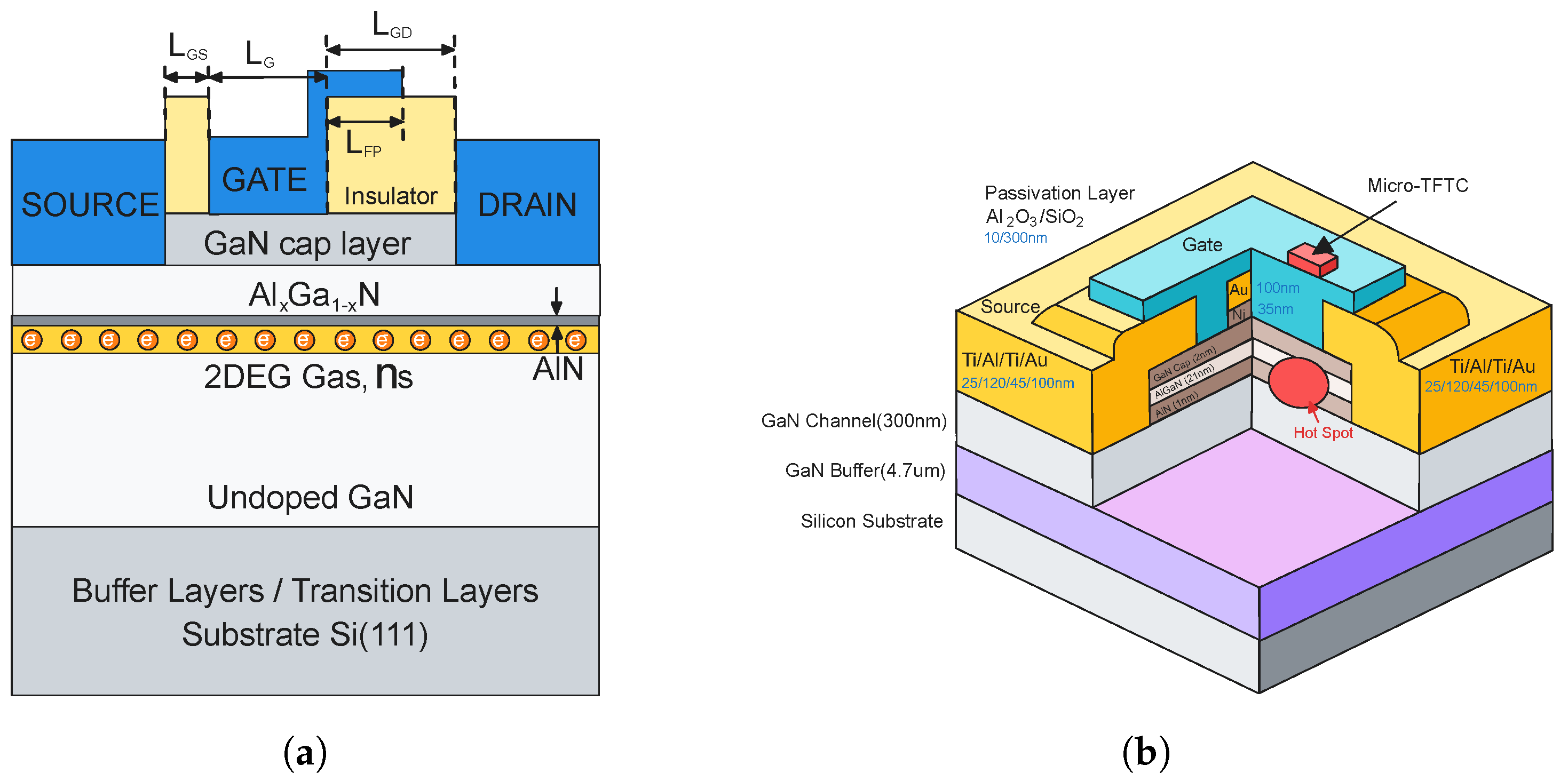
Figure 1. Structure of a GaN HEMT and an associated thermal hotspot. (a) Schematic of a GaN HEMT showing the AlGaN/GaN heterostructure and key device regions [1]. (b) Cross-section showing typical hotspot formation in the gate–drain region due to high electric fields [18].
Electronics 14 04193 g001
Figure 2. Comparison of conventional and advanced top-side interconnection technologies. (a) Conventional wire bonding, characterized by long, thin wires that introduce significant parasitic inductance and limit vertical heat dissipation [40]. (b) Advanced wire-bondless top-side interconnection (e.g., copper clips or ribbons) for reduced parasitic inductance and an improved thermal path [27].
Electronics 14 04193 g002
Figure 3. Process flow of embedded packaging technology. The sequence shows (1) die attachment, (2) lamination, (3) via drilling, (4) copper plating and structuring to form interconnections, and (5) final patterning [27].
Electronics 14 04193 g003
Figure 4. Architecture of an interleaved planar package. (a) Cross-sectional view showing the vertical arrangement of high-side and low-side MOSFETs. (b) Isometric view illustrating key components: the Interleaved Switch Unit (ISU) for thermal decoupling and the Current Commutator Structure (CCS) for current balancing [40].
Electronics 14 04193 g004
Figure 7. Chronological timeline of major packaging and cooling innovations (2010–2025).
Electronics 14 04193 g007
Table 1. Comparative and quantitative summary of advanced packaging and cooling techniques for SiC and GaN power devices, highlighting key performance improvements, advantages, trade-offs, and primary applications.
TechnologyKey Performance ImprovementsAdvantagesDisadvantages/Trade-OffsPrimary Applications
Double-Sided Cooling
  • R th reduction: 20–48% (vs. single-sided) [27,42]
  • Low L p with wire-bondless structures
  • Low overall R th
  • Uniform temperature distribution [26,51]
  • Susceptible to thermo-mechanical stress [42]
  • Requires coordinated top/bottom thermal design
  • EV/HEV traction inverters
  • High-power modules [26,50]
Embedded Packaging
  • L p reduction: up to 87.6% (<1.24 nH) [45,46,47]
  • R th reduction: 30–48% (with DSC) [42,44]
  • Very low L p
  • EMI shielding
  • Package miniaturization [46,47,48]
  • High thermo-mechanical stress
  • High process complexity and cost
  • Difficult rework [27,49]
  • High-frequency DC/DC
  • Integrated power systems [45]
Interleaved Planar
  • Thermal coupling reduction: ∼57%
  • L p as low as 3.8 nH [40]
  • Balances current/temperature in parallel devices
  • Mitigates 2D thermal coupling [40]
  • High structural complexity
  • Potential manufacturability challenges
  • High-reliability, multi-chip modules [40]
Jet Impingement
  • R th reduction: up to 64.3% (vs. indirect) [52]
  • Very high HTC
  • Effective direct hotspot cooling [52,53]
  • High pumping power required (∼5×) [52]
  • Increased system complexity
  • Potential leakage risk
  • Military and aerospace
  • Very-high-power-density electronics [52]
Microchannel
  • R th reduction: up to 43.14% (vs. indirect) [29]
  • Enables near-junction cooling
  • Shortens thermal path [29]
  • High fabrication complexity and cost
  • Large pressure drop
  • Potential channel clogging [55]
  • High-frequency RF amplifiers (e.g., GaN MMIC)
  • Dense power modules [29]
Direct Liquid
  • R th reduction: ≈30% (vs. indirect) [51]
  • Eliminates TIM layer
  • Improved heat-transfer efficiency [50]
  • CTE mismatch risk
  • Potential leakage and corrosion risk [50]
  • Automotive power modules
  • High-performance motor drives [51]
Indirect Liquid
  • Conventional baseline; moderate R th
  • Mature, reliable, cost-effective
  • Compatible with existing infrastructure [26]
  • Limited by TIM-layer resistance
  • Thermal grease degradation over time [51]
  • General-purpose industrial PSUs
  • Data center applications [26]
Disclaimer/Publisher’s Note: The statements, opinions and data contained in all publications are solely those of the individual author(s) and contributor(s) and not of MDPI and/or the editor(s). MDPI and/or the editor(s) disclaim responsibility for any injury to people or property resulting from any ideas, methods, instructions or products referred to in the content.