Article

An Optimal Operation Strategy for Surge Protective Devices in Li-Ion Based Energy Storage Systems

Department of Electrical Engineering, Korea University of Technology & Education, Cheonan 31253, Republic of Korea
*
Author to whom correspondence should be addressed.
Electronics 2025, 14(18), 3629; https://doi.org/10.3390/electronics14183629
Submission received: 31 July 2025 / Revised: 8 September 2025 / Accepted: 11 September 2025 / Published: 13 September 2025

Abstract

This paper deals with an optimal operation method for surge protective devices (SPDs) to calculate the maximum continuous operating voltage (UC) and the voltage protection level (UP) by considering the sum of the voltage protection level and the dielectric continuous voltage limit of surge protective devices in order to effectively protect energy storage system (ESS) from switching and lightning surges. This paper also implements a test device for SPDs in ESSs based on the concept of a lightning electromagnetic surge protection measurement system (LPMS) by combining an SPD coordinated with spatial shielding with an ESS configuration. Here, the test device for the SPD in the ESS is composed of a power distribution unit (PDU), uninterruptible power supply (UPS), and a lightning electromagnetic pulse (LEMP) protection device, which combines two units of SPDs and disconnection switches (DSs) connected in parallel with two units of main circuit breakers (MCBs) and noise cut transformers (NCTs) connected in series. From the test results based on the proposed optimal operation method and test device, it is clear that the residual voltage with a third-class combination waveform can be kept within 1.5 kV of the surge voltage limit in all test scenarios, and it is confirmed that the proposed test device for SPDs can protect ESSs from switching and lightning surges. Therefore, it is confirmed that the SPD tested using the proposed method can effectively reduce switching and lightning surges, while the existing SPDs installed in ESS sites cannot protect ESSs from such surges.

1. Introduction

Recently, the installation of renewable energy and energy storage systems (ESSs) has been rapidly increased to solve the crisis of global climate change. In particular, the importance of ESSs is emerging due to their multiple functions such as frequency regulation, power quality improvement, demand management, stabilization of renewable energy, and so on [1,2,3,4]. However, when lightning and switching surges are injected into the power and neutral lines, control cables, and communication line, it leads to malfunction of and damage to the ESS [5,6]. In particular, because ESSs for renewable energy are located in harsh environmental conditions, such as seaside and mountain regions, protective devices should be adopted to protect the ESS from surges [7,8]. However, it is difficult to protect the ESS from switching and lightning surges because there is no clear technical guideline for the parameter values of surge protective devices (SPDs) installed in direct current (DC) EES systems [9]. In previous studies, various methods to properly operate SPDs have been presented [10,11,12]. An optimal SPD allocation method in a low-voltage distribution system based on particle swarm optimization, an SPD selection method using EMTP S/W, and an SPD selection method according to the probability of damage were presented; however, practical research for calculating the appropriate capacity of each SPD to protect ESSs from switching and lightning surges is required.
This paper deals with an optimal surge protective device (SPD) operation method to calculate the maximum continuous operating voltage (UC) and the voltage protection level (UP) by considering the sum of the voltage protection level and the dielectric continuous voltage limit of surge protective devices in order to effectively protect ESSs from switching and lightning surges. This paper also implements a test device for SPDs in ESSs based on the concept of the lightning electromagnetic surge protection measurement system (LPMS) by combining SPDs coordinated with spatial shielding with an ESS configuration. Here, the test device for the SPD in the ESS is composed of a power distribution unit (PDU), uninterruptible power supply (UPS), and a lightning electromagnetic pulse (LEMP) protection device, which combines two units of SPDs and disconnection switches (DSs) connected in parallel with two units of main circuit breakers (MCBs) and noise cut transformers (NCTs) connected in series. From the test results based on the proposed optimal operation method and test device, it is clear that the residual voltage with a third-class combination waveform can be kept within 1.5 kV of the surge voltage limit in all test scenarios, and it is confirmed that the proposed test device for a two-port SPD can keep residual voltages within 1.5 kV of the surge voltage limit. Therefore, it is confirmed that the SPD tested using the proposed method can effectively reduce switching and lightning surges, while the existing SPDs installed in ESS sites cannot protect ESSs from such surges.

2. Operation Characteristics of SPDs in ESSs

2.1. Configuration of Subsystem in ESS

Generally, an ESS is composed of a primary subsystem, a control subsystem and an auxiliary subsystem, as shown in Figure 1. According to IEC 62933-3-1, the primary subsystem performs power conversion, the control subsystem manages the operation of the ESS, and the auxiliary subsystem provides supportive functions such as cooling and fire suppression [13]. The ESS can also be classified based on the presence or absence of auxiliary power of common (POC), which is the point where the ESS is connected to the distribution system, as shown in Figure 1a,b based on the location of the POC in subsystems using auxiliary power. Here, the ESS with auxiliary POC is generally adopted because it is difficult to apply ESSs without auxiliary POC due to the capacity of NCTs.

2.2. Protection Concepts of SPD in ESS

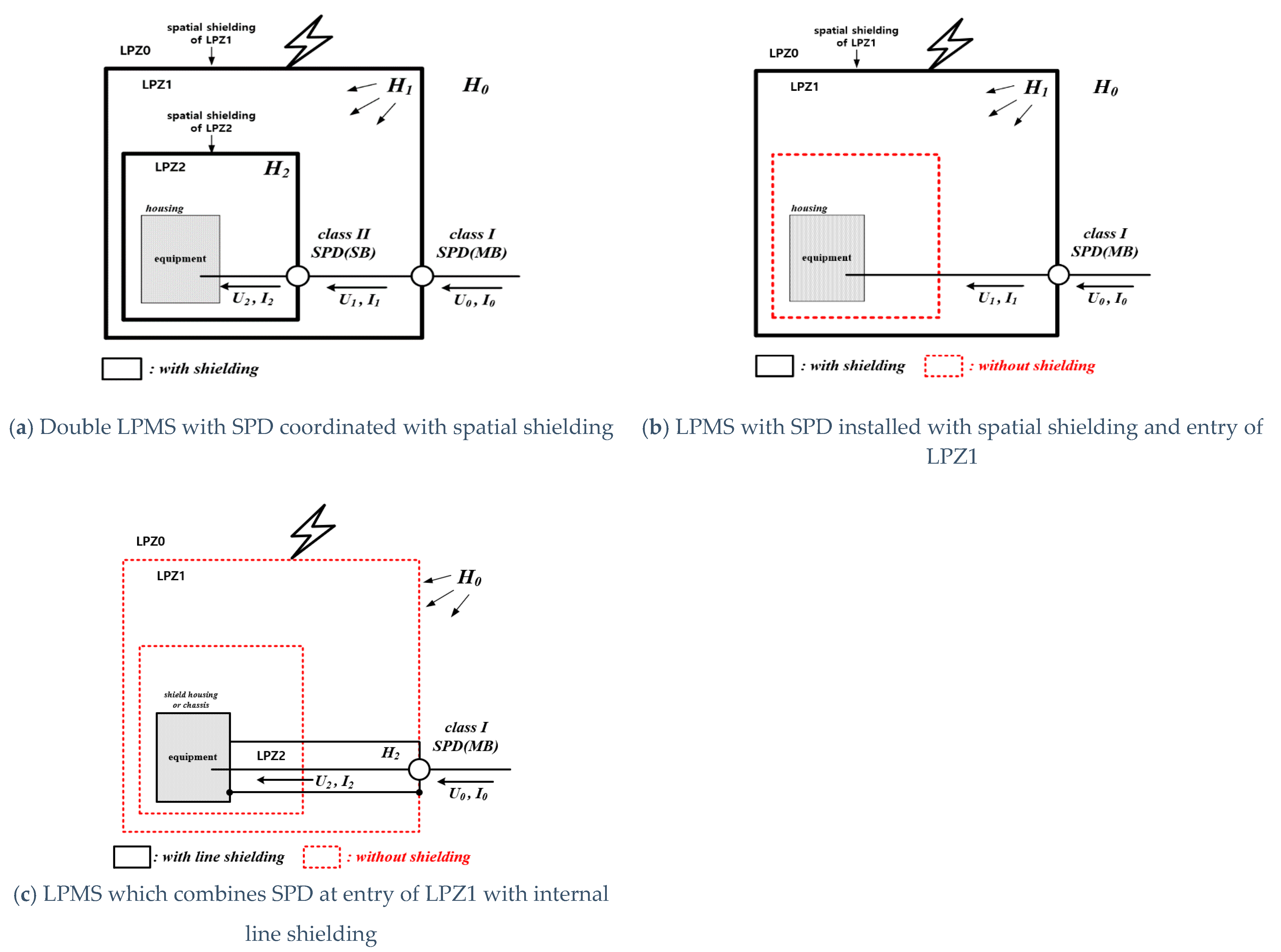
In general, lightning surges flowing into ESSs are generated by LEMP, which may cause damage to the structure and internal systems such as electrical, electronic, and communication systems [14]. In order to prevent LEMP in ESSs, this paper adapts the concept of LPMS through an SPD coordinated with spatial shielding. Namely, the LPMS is established in several forms according to the concept of the lightning protection zone (LPZ) for internal system protection, defined based on “IEC 62305-4”, as shown in Figure 2 and Table 1 [15]. Here, Figure 2a illustrates double LPMSs with SPDs coordinated with spatial shielding and Figure 2b shows an LPMS with an SPD installed with spatial shielding and the entry of LPZ1. Also, Figure 2c shows an LPMS which combines an SPD at the entrance of LPZ1 with internal line shielding. Here, Hn, Un and In represent the electromagnetic field and its induced voltage and current, respectively, which are defined in a range from 0 order to n order depending on the protection level [16].

2.3. Design of SPD in ESS

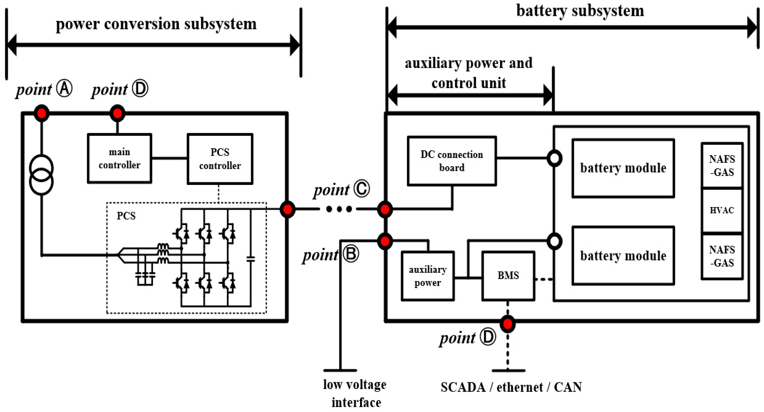
In general, the MW-scaled ESS is installed in external structures, such as containers insulated by metal housing. For example, the configuration of a container-type structure is composed of the primary subsystem, control subsystem and auxiliary subsystem in the ESS, as shown in Figure 3. Also, Table 2 shows the types of SPD based on classification of LPZs for each coupling point in Figure 3 [17].
On the other hand, Figure 4 illustrates the existing structure of an LPMS with a parallel-type one-port SPD installed with spatial shielding and the entry of LPZ1. Here, the one-port SPD is connected in parallel to the POC in the power grid, which leads to increasing residual voltage depending on the length of the connection wire of the SPD. Furthermore, it is difficult to protect the ESS from switching and lightning surges because there is no clear technical guideline for the parameter values of SPDs installed in DC systems of ESSs. Therefore, this paper deals with an optimal operation method of SPDs and implements a test device featuring a third-class combination waveform for SPDs in ESSs in order to protect the ESS from switching and lightning surges.

3. Optimal Operation Method of SPD in ESS

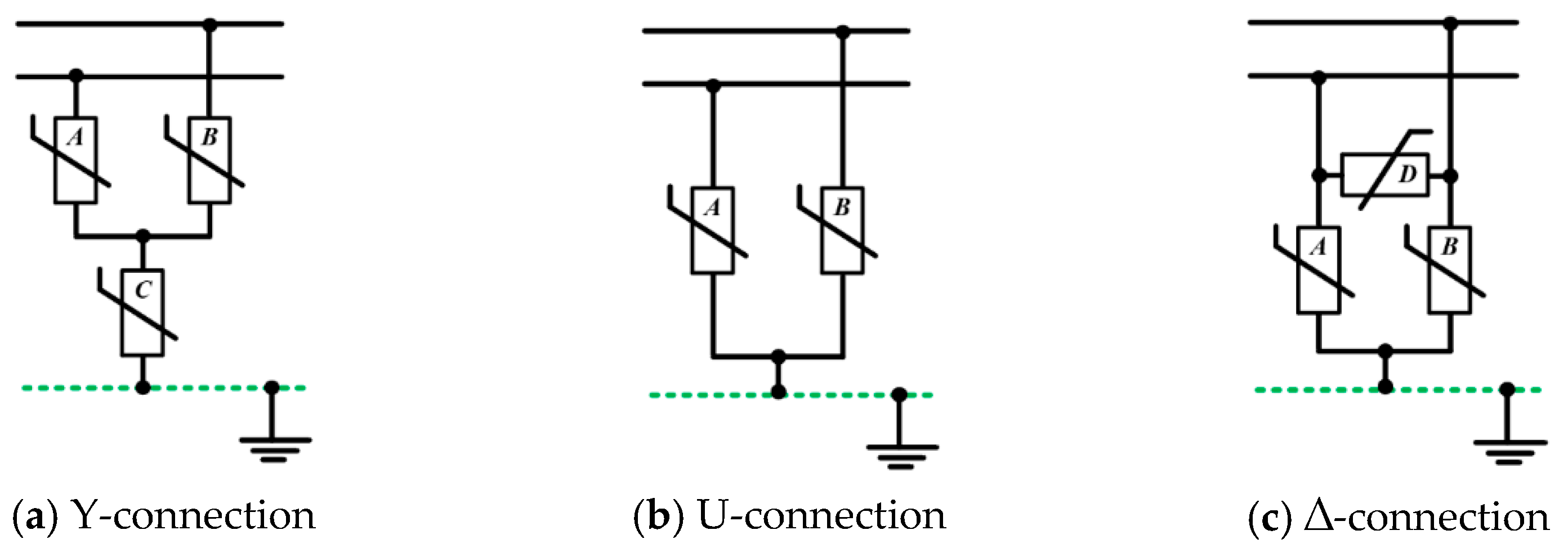
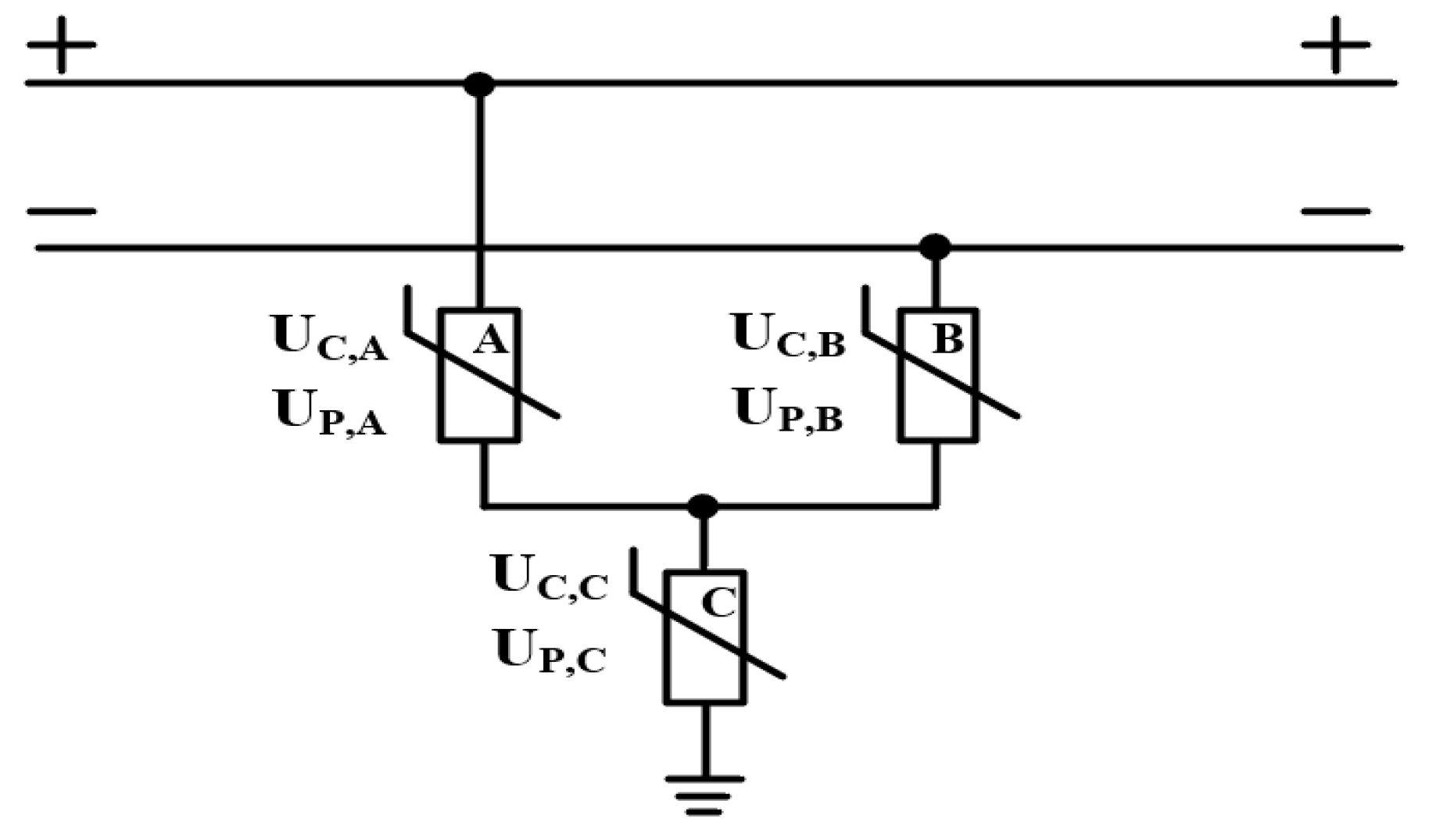
In ESS sites, Y, U, and ∆ connection types of SPDs are installed, as shown in Figure 5. Based on the Y connection type of SPD, which is mostly used in ESS sites, this paper deals with an optimal operation procedure of SPDs in ESSs as follows.
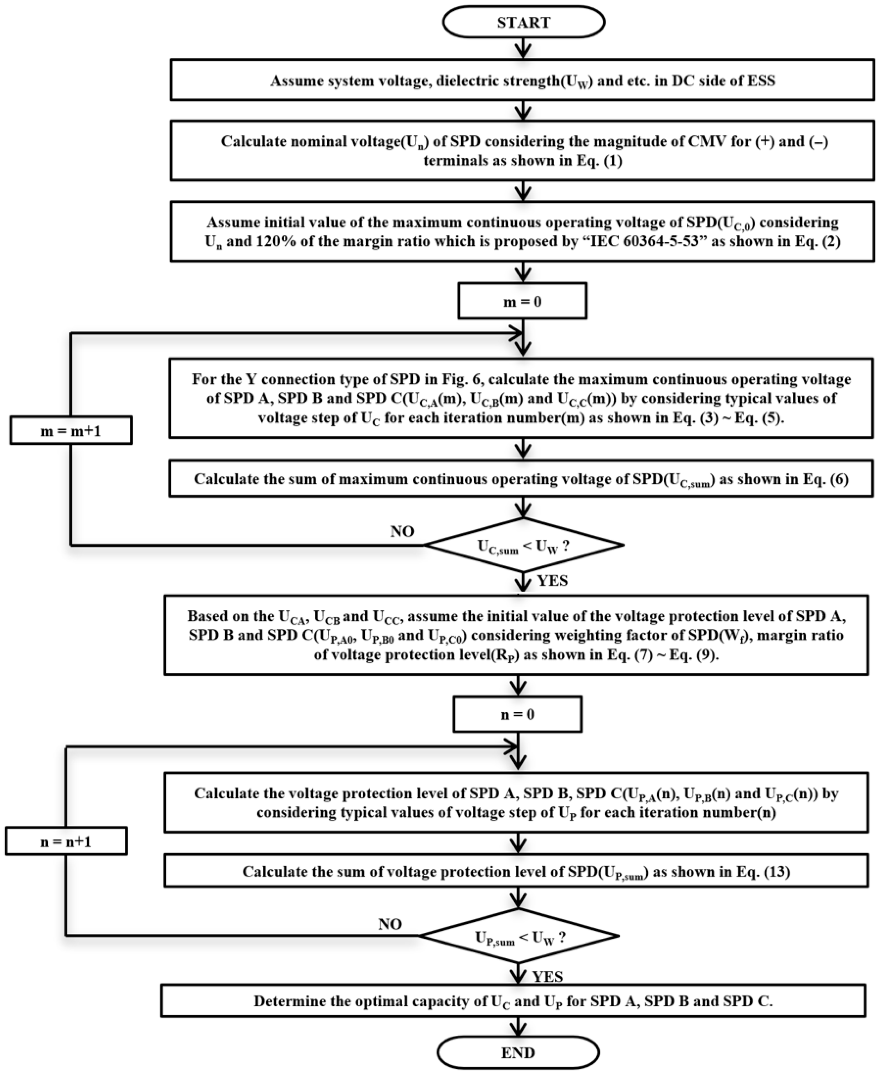
  • [Step 1] Assume system voltage, 0 dielectric strength (UW), etc., in DC side of ESS [18].
  • [Step 2] Calculate the nominal voltage (Un) of SPD considering the magnitude of CMV for (+) and (–) terminals, as shown in Equation (1). Here, the larger value of CMV is selected as Un of SPD.
    U n = m a x [ U C M V + , U C M V ]
    where Un: nominal voltage; UCMV(+): magnitude of CMV for (+) terminal; UCMV(): magnitude of CMV for (−) terminal.
  • [Step 3] Define the initial value of the maximum continuous operating voltage (UC,0) considering the nominal voltage of SPD (Un) and 120% of the margin ratio, which is proposed by “IEC 60364-5-53”, as shown in Equation (2) [14].
    U C , 0 = 1.2 × U n
    where UC,0: initial value of the maximum continuous operating voltage of SPD.
  • [Step 4] For the Y connection type of SPD in Figure 6, calculate the maximum continuous operating voltage of SPD A, SPD B and SPD C (UC,A(m), UC,B(m) and UC,C(m)) by considering typical values of voltage step of UC for each iteration number (m), as shown in Equations (3)–(5).
    Figure 6. Y connection type of SPD.
    Figure 6. Y connection type of SPD.
    Electronics 14 03629 g006
    U C , A ( m ) = U C , 0 ( Δ U C × m )
    U C , B ( m ) = U C , 0 ( Δ U C × m )
    U C , C ( m ) = U C , 0 ( Δ U C × m )
    where UC,A: UC of SPD A; UC,B: UC of SPD B; UC,C: UC of SPD C; ΔUC: typical values of voltage step of UC; m: iteration number.
  • [Step 5] Calculate the sum of maximum continuous operating voltage (UC,sum) of SPD as shown in Equation (6). If the UC,sum value is larger than the dielectric continuous voltage limit (UW) of DC system in ESS, return to [Step 4] in order to decrease UC by typical values of varying voltage (ΔUC); otherwise, go to [Step 6].
    U C , s u m = m a x [ U C , A ( m ) + U C , C ( m ) ,   U C , B ( m ) + U C , C ( m ) ]
    where UC,sum: sum of maximum continuous operating voltage of SPD.
  • [Step 6] Next, based on the UC,A, UC,B and UC,C which are obtained in [Step 5], assume the initial value of the voltage protection level of SPD A, SPD B and SPD C (UP,A0, UP,B0 and UP,C0) considering weighting factor of SPD (Wf) and margin ratio of voltage protection level (RP) as shown in Equations (7)–(9). Here, the Wf is obtained by the maximum ratio of output voltage of SPD to UC for input voltage of SPD and RP is assumed to be 120% of the typical value.
    U P , A 0 = W f × R P × U C , A ( m )
    U P , B 0 = W f × R P × U C , B ( m )
    U P , C 0 = W f × R P × U C , C ( m )
    where UP,A0: initial value of voltage protection level of SPD A; UP,B0: initial value of voltage protection level of SPD B; UP,C0: initial value of voltage protection level of SPD C; Wf: weighting factor of SPD; RP: margin ratio of voltage protection level.
  • [Step 7] Calculate the voltage protection level of SPD A, SPD B and SPD C (UP,A(n), UP,B(n) and UP,C(n)) by considering typical values of voltage step of UP for each iteration number (n) as shown in Equations (10)–(12).
    U P , A ( n ) = U P , A 0 ( Δ U P × n )
    U P , B ( n ) = U P , B 0 ( Δ U P × n )
    U P , C ( n ) = U P , C 0 ( Δ U P × n )
    where UP,A(n): UP of SPD A; UP,B(n): UP of SPD B; UP,C(n): UP of SPD C; ΔUP: typical values of voltage step of UP; n: iteration number.
  • [Step 8] Calculate the sum of the voltage protection level (UP,sum) as shown in Equation (13). If the UP,sum value is larger than the dielectric continuous voltage limit (UW) of the DC system in ESS, return to [Step 7] in order to decrease UP by typical values of voltage step (ΔUP); otherwise, go to [Step 9].
    U P , s u m = m a x [ U P , A n + U P , C n , U P , B n + U P , C n ]
    where UP,sum: sum of voltage protection level.
  • [Step 9] Finally, determine the optimal capacity of UC and UP for SPD A, SPD, B and SPD C, based on [Step 5] and [Step 8].
Therefore, the flowchart of above procedures is demonstrated as shown in Figure 7.

4. Implementation of Test Device for SPD in ESS

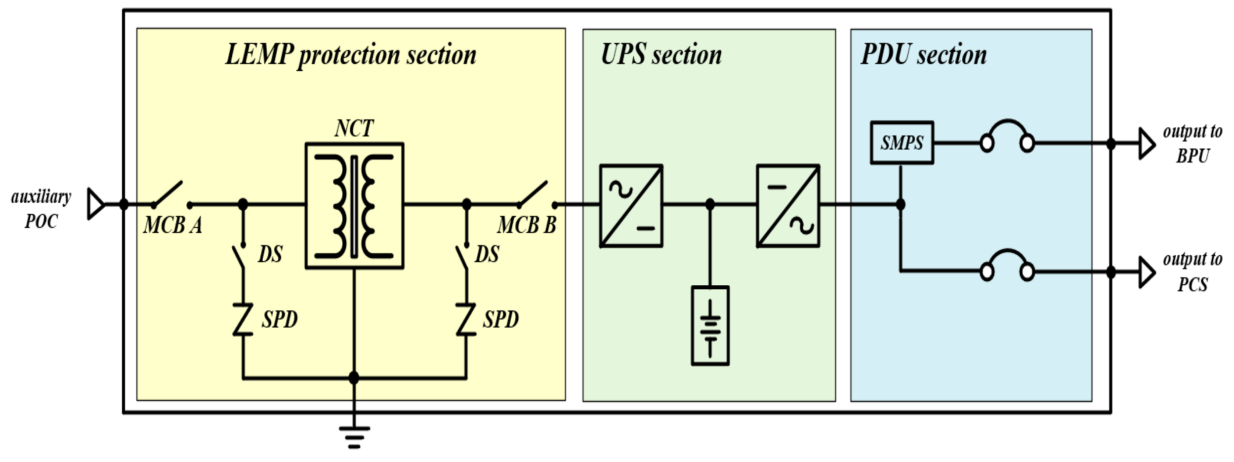
The implementation of a test device for SPDs in ESSs is illustrated as shown in Figure 8, where the test device for SPDs in ESSs is composed of PDU, UPS and LEMP protection sections. The LEMP protection section combines two units of one-port SPDs and DSs connected in parallel with two units of MCBs and NCTs in series. Furthermore, Table 3 shows the specification of the protection devices in Figure 8, which are selected by considering a 1 MW scaled power conversion system (PCS). Meanwhile, the standard for the insulation levels against voltage surge in electrical equipment connected to low-voltage systems is applied based on “IEC 60364-4-44”, as shown Table 4 [19]. Here, the surge voltage limit is selected as 1.5 kV, which corresponds to specially protected equipment at voltage levels of 230/400 V and 277/480 V.

5. Case Studies

5.1. Operation Characteristics of One-Port SPD Application

5.1.1. Test Conditions of One-Port SPD

In order to validate the optimal operation method of SPDs, this paper implements a test device which is composed of the surge generator section of a third-class combination waveform and a one-port SPD section, as shown in Figure 9. Here, the surge generator section includes a combination waveform generator of 1.5 kV, a 1.2/50 μs surge voltage, a simulated RLC device of 0.75 kA, and a 8/20 μs surge current, which are applied based on IEC 61643-11 [20]. Also, the test scenarios of the third-class combination waveform for a one-port SPD are categorized in Table 5. Here, Case I is assumed to be an existing SPD (type A) adopted at ESS sites, which has UC and UP values of 1.5 kV and 4.5 kV, respectively, and Case II is an optimal SPD (type B) selected based on the proposed operation method, which has UC and UP values of 0.8 kV and 1.5 kV, respectively.

5.1.2. Residual Voltage Characteristics of One-Port SPD

Based on the test conditions mentioned above, Figure 10 shows the residual voltage characteristics of a one-port SPD with a third-class combination waveform, measured by DEWE-571, with 300 kHz of input bandwidth and a 10 μs sampling time, which is the dominant term for peak detection. Figure 10a displays the residual voltage characteristics for the existing SPD application of Case I, and the maximum residual voltage for a 1.5 kV combination surge is obtained as 1.32 kV. Therefore, it is found that the surge protection is not performed effectively due to an 11.8% surge reduction rate, which is defined as the percentage value of reduced residual voltage with SPDs for a combination surge voltage. On the other hand, Figure 10b shows the residual voltage characteristics of the optimal SPD selected by the proposed operation method of Case II, and the maximum residual voltage for a 1.5 kV combination surge is obtained as 0.776 kV. Since the surge reduction rate is calculated as 48.2%, it is confirmed that the optimal SPD can improve the performance of SPDs by 36.4% compared to the existing SPDs and thus properly reduce switching and lightning surges.

5.2. Operation Characteristics of Two-Port SPD Application

5.2.1. Test Conditions of Two-Port SPD

This paper implements a test device to evaluate operation characteristics of a two-port SPD for an ESS, as shown in Figure 11. The test conditions of the third-class combination waveform for the two-port SPD are assumed as shown in Table 6. In order to evaluate whether the residual voltages are kept within the 1.5 kV surge voltage limit, the injection waveforms for the test conditions are applied based on “IEC 61643-11” and “IEEE C62.41”, and the measurement points are set to SPDs on primary and secondary sides [20,21]. From the test conditions, the test scenarios of the third-class combination waveform for a two-port SPD are categorized in Table 7, where Case III represents the voltage and current of the combination waveform, defined as 6 kV and 3 kA, respectively, based on condition C1 in IEEE C62.41. Also, Case IV and Case V are determined based on the C2 and C3 conditions.

5.2.2. Residual Voltage Characteristics of Two-Port SPD

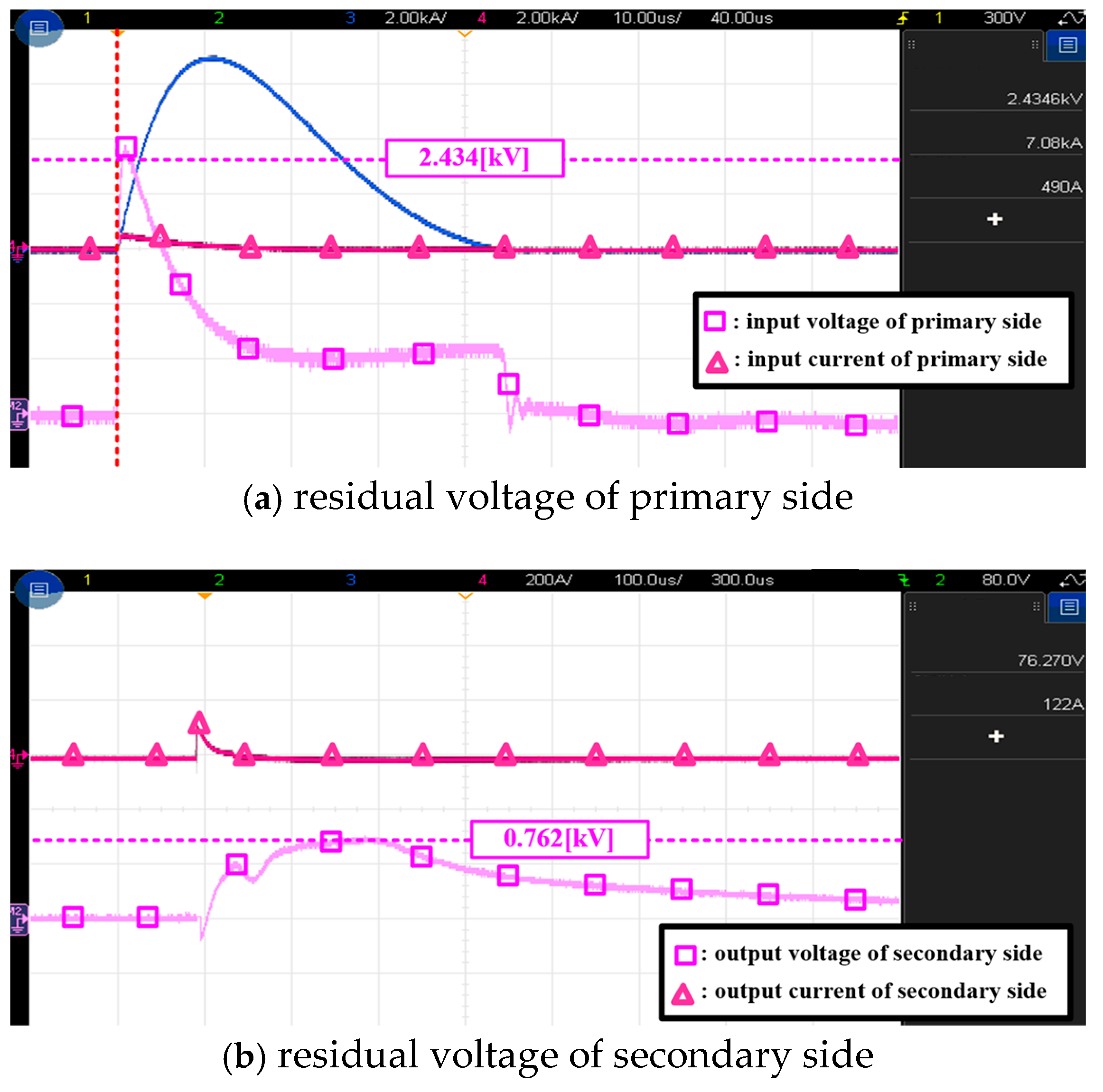
From the test results according to the test conditions mentioned above, the residual voltage characteristics with the third-class combination waveform in Case V are obtained as shown in Figure 12, where Figure 12a,b are the residual voltage characteristics of the SPDs on the primary and secondary sides, respectively. The maximum residual voltage of the SPD on the primary side for a 20 kV combination surge is obtained as 2.434 kV, with a value of 0.762 kV on the secondary side. Furthermore, it is known that the total surge reduction rate is calculated as 96.2%, and the residual voltage is kept within required surge voltage limit. Therefore, it is confirmed that the proposed two-port SPD can effectively reduce surges and then protect ESSs from switching and lightning surges.
Furthermore, the residual voltage characteristics with the third-class combination waveform in all cases are summarized in Table 8. The maximum residual voltages of SPDs on the primary and secondary sides in Case III are obtained as 1.169 kV and 0.501 kV, and the maximum residual voltages in Case IV are 1.577 kV and 0.682 kV, respectively. Therefore, it is clear that the residual voltage with a third-class combination waveform can be kept within 1.5 kV of the surge voltage limit in all test scenarios, and it is confirmed that the proposed test device for a two-port SPD can keep residual voltages within 1.5 kV of the surge voltage limit, and thus the ESS can be safety protected from switching and lightning surges.

6. Conclusions

This paper deals with an optimal operation method for SPDs and implements a test device featuring a third-class combination waveform for SPDs in ESSs in order to protect the ESS from switching and lightning surges. The main results are summarized as follows:
(1)
For the existing SPD application of Case I, the maximum residual voltage for a 1.5 kV combination surge with a third-class combination waveform is obtained as 1.32 kV, and thus it is found that surge protection is not performed effectively due an 11.8% surge reduction rate.
(2)
On the other hand, the maximum residual voltage for the optimal SPD application of Case II, selected based on the proposed operation method, is obtained as 0.776 kV, and the surge reduction rate is calculated as 48.2%. Therefore, it is confirmed that the optimal SPD in ESSs can properly reduce switching and lightning surges.
(3)
From the test results for a two-port SPD with a third-class combination waveform, the maximum residual voltage of the primary-side SPD for a 20 kV combination surge is obtained as 2.434 kV, with a value of 0.762 kV for the secondary-side SPD, and the total surge reduction rate is calculated as 96.2%.
(4)
Therefore, it is confirmed that the SPD tested using the proposed method can effectively reduce surges, while the existing SPDs installed in ESS sites may not protect ESSs from switching and lightning surges.
(5)
The proposed SPD for ESSs can keep maximum residual voltages within 1.5 kV of the surge voltage limit, and thus the ESS can be safety protected from switching and lightning surges.
(6)
This study has focused on an operation method for surge protective devices in ESSs; research on strategies for the commercialization of the proposed device in terms of economy and reliability will be performed in the near future.

Author Contributions

Y.-H.K. conceptualized the study and led the writing of the manuscript. H.-S.Y. performed data analysis. M.-H.L. and S.-E.R. contributed to the literature review and methodology. S.-J.K. assisted with data collection and D.-S.R. supervised the overall project and revised the manuscript critically. All authors have read and agreed to the published version of the manuscript.

Funding

This research was supported by Korea Institute of Energy Technology Evaluation and Planning (KETEP) grant funded by the Korea Government (MOTIE) (20224000000160, DC Grid Energy Innovation Research Center and this research was supported the Korea Institute of Energy Technology Evaluation and Planning (KETEP) grant funded by the Korea Government (MOTIE) (RS-2024-00421994, Development of performance verification techniques and safety evaluation system for LiB-UPS System unit).

Data Availability Statement

Data are contained within the article.

Acknowledgments

All author have reviewed and edited the output and take full responsibility for the content of this publication.

Conflicts of Interest

The authors declare no conflicts of interest.

References

  1. Chen, J.; Liu, Y.; Bao, G. Optimal operating strategy for distribution networks with PV and BESS considering flexible energy storage. In Proceedings of the 2016 IEEE Power and Energy Society General Meeting (PESGM), Boston, MA, USA, 17–21 July 2016; pp. 1–5. [Google Scholar]
  2. Xiong, P.; Singh, C. Optimal Planning of Storage in Power Systems Integrated with Wind Power Generation. IEEE Trans. Sustain. Energy 2016, 7, 232–240. [Google Scholar] [CrossRef]
  3. Kim, Y.H.; Myung, H.S.; Kang, N.H.; Lee, C.W.; Kim, M.J.; Kim, S.H. Operation Plan of ESS for Increase of Acceptable Product of Renewable Energy to Power System. Trans. Korean Inst. Electr. Eng. 2018, 67, 31–40. [Google Scholar]
  4. Kim, Y.M.; Son, B.S.; Kim, S.H. Operation Planning and Capacity Calculation of Energy Storage Systems Considering Curtailment of Renewable Energy. J. Korean Sol. Energy Soc. 2023, 43, 1–12. [Google Scholar]
  5. Matsuura, S.; Kanatani, K. Characteristics of Damages of Distribution Lines Due to Lightning in Hokuriku Area of Japan. In Proceedings of the 2023 12th Asia-Pacific International Conference on Lightning (APL), Langkawi, Kedah, 12–15 June 2023. [Google Scholar]
  6. Cho, S.D.; Shen, J.; Choi, S.M.; Han, B.G.; Rho, D.S. A Study on Mechanism and Modeling of CMV in Sharing Energy Storage System. J. Korea Acad. Ind. Coop. Soc. 2023, 24, 616–625. [Google Scholar] [CrossRef]
  7. Zaini, N.H.; Ab-Kadir, M.Z.A.; Radzi, M.A.A.; Izadi, M.; Ahmad, N.I.; Azis, N.; Nasir, M.S.M. On the Effect of Surge Protection Devices (SPDs) Placement for Grid-connected Solar PV Farm. In Proceedings of the 2018 34th International Conference on Lightning Protection (ICLP), Rzeszow, Poland, 2–7 September 2018. [Google Scholar]
  8. Kim, J.Y.; Choi, S.J.; Kim, J.H.; Lee, G.H.; Jung, J.S.; Shong, K.M. Analysis of Accident Cases and Development of Safety Standards for LiB-based Energy Storage Technology. Trans. Korean Inst. Electr. Eng. 2023, 72, 1760–1767. [Google Scholar] [CrossRef]
  9. Luo, S.; Wang, Z.; Ren, Y.; Wang, H. Research on Follow-current Interruption Capacity of Switching Type SPD for Low-voltage Distribution Systems Used in Telecommunication Stations. In Proceedings of the 2024 4th International Conference on Electronics, Circuits and Information Engineering (ECIE), Hangzhou, China, 1–3 March 2024; pp. 175–180. [Google Scholar]
  10. Yan, N.; Qing, Y.; Yao, Z.; Li, Z.; Kaifang, Z. Optimal Allocation of SPD in Low Voltage Distribution System Based on Particle Swarm Optimization. In Proceedings of the 2017 Chinese Automation Congress (CAC), Jinan, China, 20–22 October 2017; pp. 4015–4018. [Google Scholar]
  11. Milardic, V.; Uglesic, I.; Pavic, I. Selection of Surge Protective Devices for Low-Voltage Systems Connected to Overhead Line. IEEE Trans. Power Deliv. 2010, 25, 1530–1537. [Google Scholar] [CrossRef]
  12. Piparo, G.B.L.; Kisielewicz, T.; Mazzetti, C.; Rousseau, A. Selection procedures for surge protective devices according to the probability of damage. Electr. Power Syst. Res. 2017, 146, 321–330. [Google Scholar] [CrossRef]
  13. IEC 62933-3-1; Electrical Energy Storage (EES) Systems—Part 3-1: Planning and Performance Assessment of Electrical Energy Storage Systems. IEC: Geneva, Switzerland, 2018.
  14. IEC 62305-1; Protection Against Lightning—Part 1: General Principles. IEC: Geneva, Switzerland, 2024.
  15. IEC 62305-4; Protection Against Lightning—Part 4: Electrical and Electronic Systems Within Structures. IEC: Geneva, Switzerland, 2024.
  16. IEC 61643-12; Low-Voltage Surge Protective Devices—Part 12: Surge Protective Devices Connected to Low-Voltage Power Systems—Selection and Application Principles. IEC: Geneva, Switzerland, 2020.
  17. IEC 60099-7; Surge Arresters—Part 7: Glossary of Terms and Definitions. IEC: Geneva, Switzerland, 2004.
  18. IEC 60364-5-53; Low-Voltage Electrical Installations—Part 5-53: Selection and Erection of Electrical Equipment—Devices for Protection for Safety, Isolation, Switching, Control and Monitoring. IEC: Geneva, Switzerland, 2024.
  19. IEC 60364-4-44; Low-Voltage Electrical Installations—Part 4-44: Protection for Safety—Protection Against Voltage Disturbances and Electromagnetic Disturbances. IEC: Geneva, Switzerland, 2024.
  20. IEC 61643-11; Low-Voltage Surge Protective Devices—Part 11: Surge Protective Devices Connected to Low-Voltage Power Systems—Requirements and Test Methods. IEC: Geneva, Switzerland, 2011.
  21. IEEE C62.41; IEEE Recommended Practice for Surge Voltages in Low-Voltage AC Power Circuits. IEEE: Piscataway, NJ, USA, 1991.
Figure 1. Configuration of ESS.
Electronics 14 03629 g001
Figure 2. Concepts of LPMS protection method.
Electronics 14 03629 g002
Figure 3. Architecture of container-type ESS.
Electronics 14 03629 g003
Figure 4. Protection design of ESS with LPMS.
Electronics 14 03629 g004
Figure 5. Connection types of SPD.
Electronics 14 03629 g005
Figure 7. Optimal operation method of SPD in ESS.
Electronics 14 03629 g007
Figure 8. Configuration of test device for SPD in ESS.
Electronics 14 03629 g008
Figure 9. Configuration of 1-port SPD test device.
Electronics 14 03629 g009
Figure 10. Residual voltage characteristics of 1-port SPD.
Electronics 14 03629 g010
Figure 11. Configuration of test device for 2-port SPD.
Electronics 14 03629 g011
Figure 12. Residual voltage characteristics of 2-port SPD.
Electronics 14 03629 g012
Table 1. Classification of LPZ.
ZonesDefinition
LPZ0Azone where the threat is due to direct lightning flash and the full lightning electromagnetic field, the internal systems may be subjected to full lightning
LPZ0Bzone protected against direct lightning flashes but where the threat is the full lightning electromagnetic field; the internal systems may be subjected to partial lightning current
LPZ1zone where the surge current is limited by current sharing and by SPDs at the boundary, spatial shielding may attenuate the lightning electromagnetic field
LPZ2…nzone where the surge current may be further limited by current sharing and by additional SPDs at the boundary, additional spatial shielding may be used to further attenuate the lightning electromagnetic field
Table 2. Classification of SPD types for LPZs.
SPD
Type
Identification of LPZCoupling
Point
class Izone protected against direct lightning flashes but where the threat is the full lightning electromagnetic field
class IIzone where the surge current is limited by current sharing and by SPDs at the boundary
class IIIzone where the surge current may be further limited by current sharing and additional SPDs at the boundary and additional spatial shielding may be used to further attenuate the lightning electromagnetic fieldⒸ, Ⓓ
Table 3. Specification of test device for SPD in ESS.
ItemsSpecification
MCBrated current (In)50 A
rated insulation voltage (Ui)750 V
rated surge voltage limit (Uimp)8 kV
SPD DSnominal surge discharge current (In)20 kA, 8/20 μs
maximum surge discharge current (Imax)40 kA, 8/20 μs
maximum continuous operating voltage (Uc)600 V
SPDnominal surge discharge current (In)20 kA, 8/20 μs
maximum surge discharge current (Imax)40 kA, 8/20 μs
maximum continuous operating voltage (Uc)320 V
protection voltage level (Up)1.5 kV
NCTcapacity5 kVA
winding type1 P, 2 W
Table 4. Voltage limit levels.
Nominal Voltage of Installation [V]Required Rated Surge Voltage Limit of Equipment [kV]
3-Phase
Systems
1-Phase
Systems
Equipment at the Origin of InstallationEquipment of Distribution and Final CircuitAppliances and Current Using EquipmentSpecially Protected Equipment
-120–24042.51.50.8
230/400
277/480
-642.51.5
400/690-8642.5
1000-12864
Table 5. Test scenarios of 3rd-class combination waveform for 1-port SPD.
CaseParameter Value of SPD
UC [kV]UP [kV]
I1.54.5
II0.81.5
Table 6. Test conditions of 3rd-class combination waveform for 2-port SPD.
ItemsContents
injection waveformcombination waveform of voltage pulse (1.2/50 μs) and current pulse (8/20 μs)
injection terminalsL-N
exposure levelC1, C2, C3
measurement pointSPD on primary and secondary sides
Table 7. Test scenarios of 3rd-class combination waveform for 2-port SPD.
CaseCombination
Waveform Voltage [kV]
Combination
Waveform Current [kA]
III63
IV105
V2010
Table 8. Test scenarios of 3rd-class combination waveform for 2-port SPD.
CasePrimary-Side
Voltage [kV]
Secondary-Side
Voltage [kV]
III1.1690.501
IV1.5770.682
V2.4340.762
Disclaimer/Publisher’s Note: The statements, opinions and data contained in all publications are solely those of the individual author(s) and contributor(s) and not of MDPI and/or the editor(s). MDPI and/or the editor(s) disclaim responsibility for any injury to people or property resulting from any ideas, methods, instructions or products referred to in the content.