Article

AFSS Wide-Frequency Reconfigurable Design and Electromagnetic Characterization Research

1
School of Photoelectric Engineering, Xi’an Technological University, Xi’an 710021, China
2
School of Computing, Engineering and Physical Sciences, University of the West of Scotland, Paisley PA1 2BE, Scotland, UK
*
Author to whom correspondence should be addressed.
Electronics 2025, 14(18), 3628; https://doi.org/10.3390/electronics14183628 (registering DOI)
Submission received: 6 August 2025 / Revised: 7 September 2025 / Accepted: 10 September 2025 / Published: 12 September 2025

Abstract

In order to solve the dynamic adaptation problem of the working frequency band of the FSS in the complex electromagnetic environment and further expand the frequency tuning range, a reconfigurable AFSS unit model based on PIN and varactor diodes are designed, which can achieve the insertion loss below−1 dB in the wide frequency range of 10.2–15.2 GHz, meet the working-band switching, and allow for flexibly adjusting the working frequency point. In order to verify the accuracy of the design method, a square-ring aperture and notched patch-coupling structure that can exhibit broadband transmission response in the X-Ku band is first proposed based on the equivalent circuit model topology. A numerical simulation and a processing test of the structure are carried out. The measured data are in good agreement with the simulation results. After optimizing the unit structure, different capacitance values and resistance values are added to the diodes in the numerical simulation to control the equivalent PIN diode switch and the capacitance change in the varactor diodes. According to the equivalent circuit model and the electric-field intensity distribution, the AFSS regulation mechanism of the loaded diodes is explored. In this paper, through numerical simulation optimizations and experimental verification, the design method and performance optimization strategy of frequency-tunable FSS in the working range of 2–18 GHz are systematically studied, which provides theoretical support for the design of electromagnetic functional devices in the new generation of communication, radar, and electronic warfare systems.

1. Introduction

Frequency-selective surfaces (FSS) are two-dimensional periodic artificial electromagnetic structures with spatial filtering characteristics. They comprise subwavelength-sized metal patches or aperture units arranged in a specific spatial period [1]. Under ideal conditions, FSS reflect or transmit electromagnetic signals within designated frequency bands without absorbing energy. Through optimized structural design, precise regulation of electromagnetic waves can be achieved.
Contemporary military radar antennas and wireless communication systems increasingly demand broadband and frequency-agile operation. Most traditional FSS are designed for fixed-frequency bands and struggle to adapt to dynamic requirements in complex electromagnetic environments. To address this, active frequency-selective surfaces (AFSS) integrate electronic control devices into traditional structures. By adjusting external excitation, AFSS dynamically modify electromagnetic performance to achieve reconfigurable characteristics [2,3]. Among methods for realizing AFSS reconfigurability [4,5,6], designs incorporating PIN diodes or varactor diodes offer advantages including rapid frequency response, flexible functionality switching, and low fabrication costs, enhancing practicality [7,8,9]. Early work by Ghaffer et al. (2007) [10] loaded PIN diodes onto a single-layer FSS structure, demonstrating electromagnetic property switching via diode on/off control. In 2011, Withayachumnankul [11] achieved wideband tunable performance (2.7–3.5 GHz) by loading varactor diodes into an AFSS parallel resonant unit. Subsequently, Amir Ebrahimi et al. (2016) [12] proposed a bandpass FSS with variable capacitance tuning, exhibiting nearly constant bandwidth across a 3.7–5.2 GHz tuning range. The development of active frequency-selective surfaces (AFSS) has seen continuous advances in multi-function integration and tuning performance. In 2019, Ratanak P. et al. developed a multifunctional AFSS (MAFSS) utilizing active switching devices [13]. Also, that year, Li Huangyan et al. from Nanjing University of Aeronautics and Astronautics proposed a resonant model incorporating both PIN and varactor diodes, achieving multiple reconfigurable functions—including transmission/reflection switching, polarization selection, and frequency tuning—within the 1.3–2.1 GHz band [14]. In 2021, Hui Bai’s team introduced a tunable FSS with stable angular performance up to 45° incidence [15]. He Zhangjian (2022) further optimized the bias network for miniaturization, enabling a PIN-based reconfigurable AFSS with broadband switching (4.2–5 GHz) and frequency tuning (2.17–4.8 GHz), while maintaining stability up to 60° incidence [16].
Subsequent studies further extended structural and functional diversity. Li Huan’s group from Zhejiang University designed a stacked AFSS with three non-resonant metal layers and two dielectric substrates, using varactors to continuously tune the passband from 4.0 GHz to 5.8 GHz [17]. A 2023 study reported a varactor-tuned bandpass AFSS with reconfigurable transmission between 3.4 and 6.4 GHz and enhanced out-of-band RCS suppression, albeit with insertion loss ranging from 0.6 dB to 5.1 dB [18]. In 2024, a PIN-diode-based AFSS was proposed as a passband switch [19]; however, its binary ON/OFF states limited functionality to transmission blocking without continuous tuning or multi-dimensional control. That same year, a dual-passband AFSS with an LC-L resonant circuit achieved independent tuning in both low (1.69–2.99 GHz) and high (4.03–5.54 GHz) bands [20].
Despite these advances, conventional AFSS designs still face inherent limitations: most support only single-frequency tuning within narrow ranges, and the incorporation of multiple active elements often leads to increased insertion loss. A central challenge remains in realizing wide-range frequency reconfigurability with minimal loss and stable angular performance under complex electromagnetic conditions. The main content of this paper focuses on integrating varactor diodes and PIN diodes to design an active frequency-selective surface (AFSS) structure capable of cross-band and wide-range frequency tuning, leveraging the ON/OFF characteristics of PIN diodes and the tuning performance of varactor diodes. Compared to single-frequency tunable AFSS designs, this cross-band widely tunable AFSS model is better suited to meet the demands of military radar and communication development, offering broader application prospects [21]. Starting from theoretical studies, simulation modeling, and experimental validation, a second-order circuit model is first transformed into a unit structure. By comparing numerical simulations with experimental test results, feasibility is verified for subsequent AFSS design work. Secondly, an optimized reconfigurable unit cell is developed by integrating PIN diodes and varactor diodes, alongside a rationally designed bias network to minimize additional insertion loss. This structure achieves passband tuning with insertion loss better than −1 dB across 10.2–15.2 GHz through capacitor adjustment and switch control. Switching between two operational bands (X-band to Ku-band) is realized by toggling the PIN diode states, while continuous frequency tuning within each band is enabled by adjusting the varactor diode bias voltage. The operating mechanism of the AFSS is elucidated through equivalent circuit modeling and electric-field distribution analysis, providing valuable insights for flexible frequency control in AFSS technology.

2. Verification of Design Principles and Methods

2.1. Equivalent Circuit Method

In the study of periodic FSS array structures, the equivalent circuit method (ECM) provides an efficient and intuitive approximation. Based on quasi-static electromagnetic field assumptions, ECM models the FSS unit cell as a lumped-parameter circuit equivalent to a transmission line model [22,23]. This study employs ECM to develop the basic unit-cell topology, enabling rapid calculation of FSS resonant characteristics from equivalent circuit parameters.
As shown in Figure 1, for a square-ring aperture array, when the gap of the aperture is much smaller than the size of the periodic element, the square-ring aperture can be equivalent to an LC parallel circuit, and its equivalent circuit impedance satisfies Equation (1):
1 Z = 1 Z L + 1 Z C
The impedance expressions for the inductor and capacitor are given by Equations (2) and (3), respectively.
Z L = j w L
Z c = 1 j w C
Substitute expressions Equations (2) and (3) into Equation (1) to derive the circuit impedance, which satisfies the following conditions:
Z = 1 1 Z L + 1 Z C = 1 1 j ω L + j ω C
When the impedance Z in Equation (4) tends to infinity, the resonant frequency f 0 satisfies:
f 0 = ω 2 π = 1 2 π L C
According to circuit theory, when the input frequency equals the resonant frequency, the inductive and capacitive impedances balance each other. At resonance, the equivalent impedance becomes theoretically infinite, and currents through the inductor and capacitor exhibit equal magnitude but opposite phase. Consequently, the AC signal cannot shunt to ground through the LC parallel circuit. Under this condition, the square-ring aperture array (FSS) exhibits bandpass characteristics at the resonant frequency.
In order to clarify the relationship between structural dimensions and equivalent capacitance, inductance, empirical formulas for calculating these parameters have been developed. The following approximations provide relatively accurate equivalent inductance (L) and capacitance (C) values for surface-mounted metallic unit cells [24]:
L = μ 0 D 2 π log 2 sin π w 2 D
C = ε 0 ε eff 2 D π log 2 sin π s 2 D
The meanings of each parameter are shown in Figure 1a above, where D , w , and s are the length, width, and gap interval of the metal strip, respectively, ε e f f is the effective dielectric constant of the dielectric layer; ε 0 is the dielectric constant in vacuum; μ 0 is the magnetic permeability in vacuum.
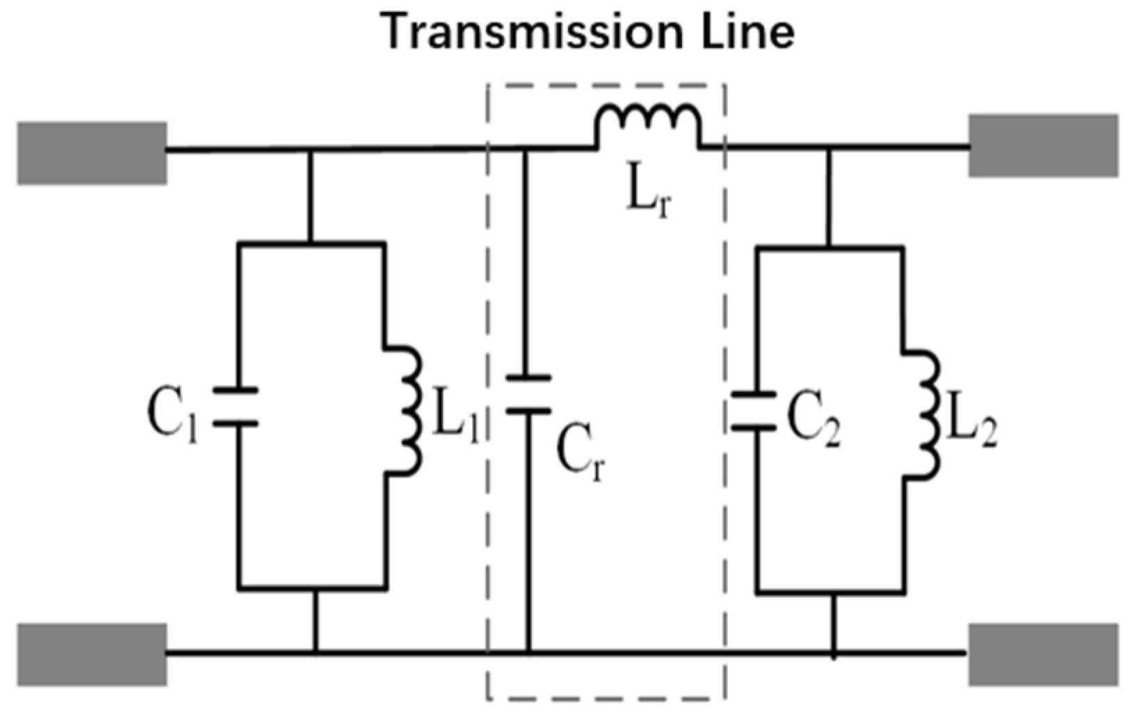
A typical LC parallel circuit yields only a single bandpass resonance. According to filter theory, although first-order filter models benefit from structural simplicity, they suffer from broad transition bands and inadequate stopband attenuation, resulting in limited filtering performance [25]. To improve the frequency-selective characteristics of the FSS, multiple LC parallel resonant circuits can be cascaded to achieve higher-order filtering responses [26,27]. This section employs a second-order filter model, implemented in the FSS as a double-layer cascaded metallic patch structure. As illustrated in Figure 2, the equivalent circuit of this second-order configuration is shown. The aperture structures on both sides are modeled as parallel L1C1 and L2C2 circuits, respectively, while the dielectric substrate is represented as a transmission line with specific characteristic impedance, equivalent to a parallel capacitor Cᵣ and a series inductor Lᵣ.

2.2. Structural Design and Numerical Simulation Research

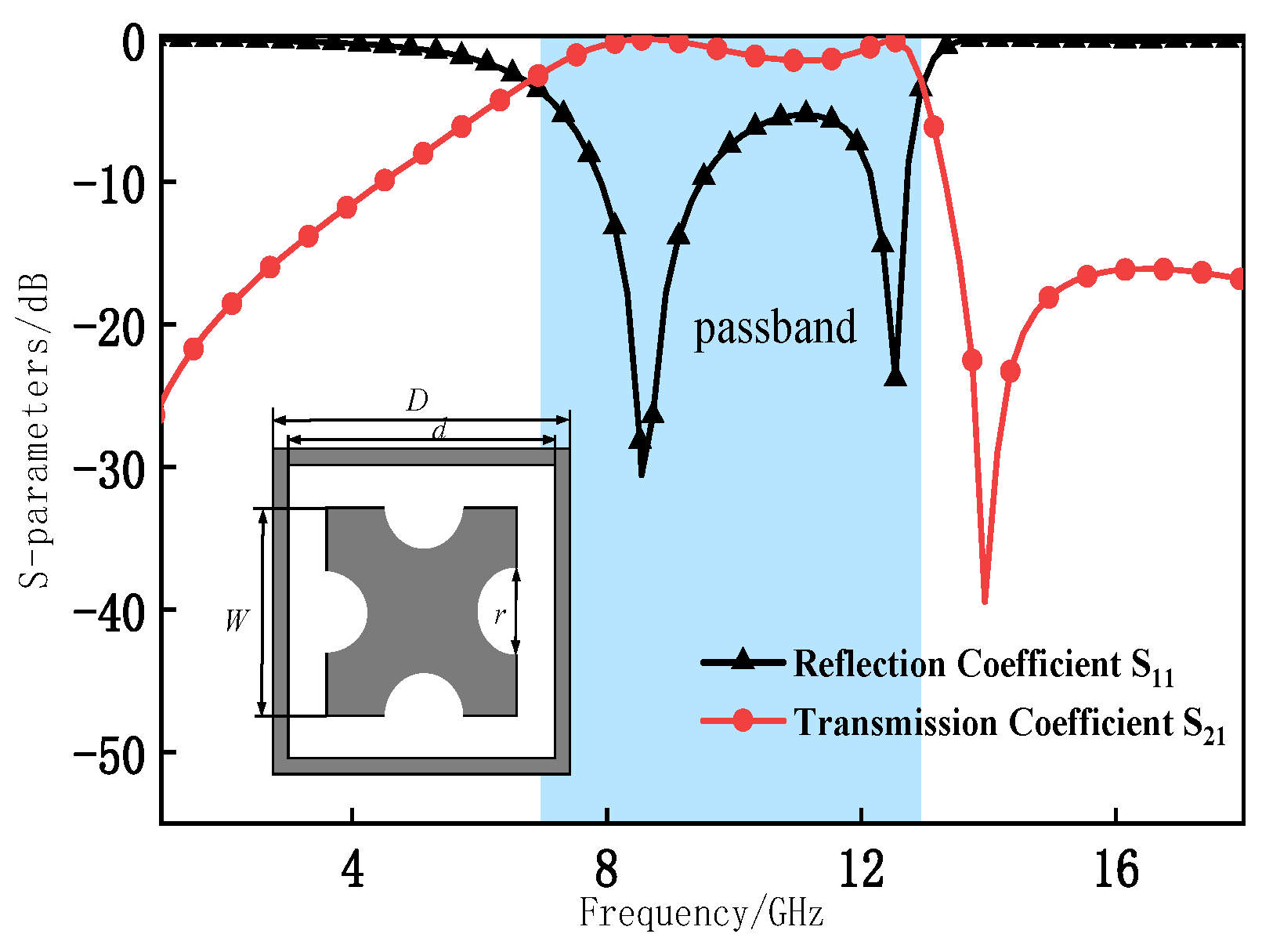
The structural topology is applied to the equivalent circuit model in Figure 2. Compared to other unit types, the annular structure suppresses premature excitation of higher-order harmonics while demonstrating superior frequency-response stability. Consequently, a novel structure featuring coupled square-ring apertures and notched patches is designed, based on a conventional square-ring unit. Figure 3 presents the designed unit structure model. The specific structural dimensions after optimization are shown in Table 1, and the medium substrate material selected is TLY-5.
Numerical simulations of the initial structure were performed using CST Studio Suite v2018. Figure 4 shows the transmission and reflection coefficients under normal TE-polarized wave incidence. Mutual coupling between the dual-layer resonators expands the bandwidth and sharpens the roll-off characteristics. The −1.5 dB bandwidth measures 5.4 GHz (7.4–12.8 GHz), corresponding to a 53.5% fractional bandwidth. This structure exhibits excellent in-band performance with low insertion loss and high transmission efficiency, while the stopband demonstrates a flat reflection coefficient profile and strong out-of-band suppression.
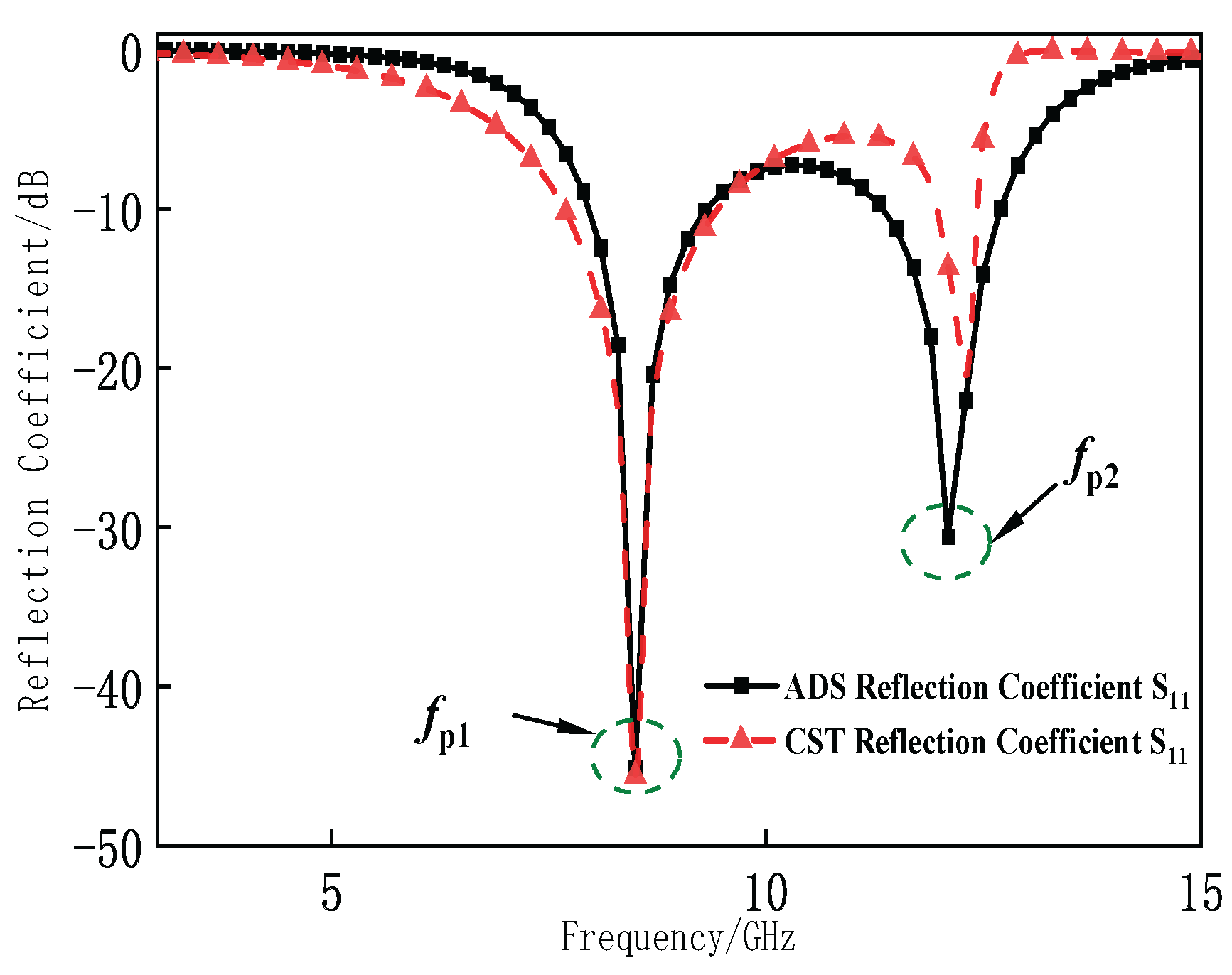
For numerical modeling, electromagnetic simulations were primarily performed using CST Studio Suite (CST Studio Suite, based on the Finite-Difference Time-Domain method, is manufactured by Dassault Systèmes, whose headquarters is located in Paris, France). Complementary verification employed ADS (Advanced Design System) implementing the equivalent circuit method (ECM). The equivalent circuit model in Figure 2 was implemented in ADS to compute S-parameters. Figure 5 compares simulated results from CST and ADS. For analytical clarity, only the reflection coefficient (S11) is shown.
Comparative analysis reveals close agreement between the reflection coefficient curves obtained from both software simulations, with strong correlation in overall results. Minor discrepancies occur at the second resonant frequency due to electromagnetic coupling effects between unit cells and layers in the FSS structure—a phenomenon not captured in the equivalent circuit model optimization. Although slight parameter variations exist between circuit-optimized and full-wave-optimized values, the equivalent circuit method remains effective for rapid FSS design iteration.

2.3. Angular Stability Validation

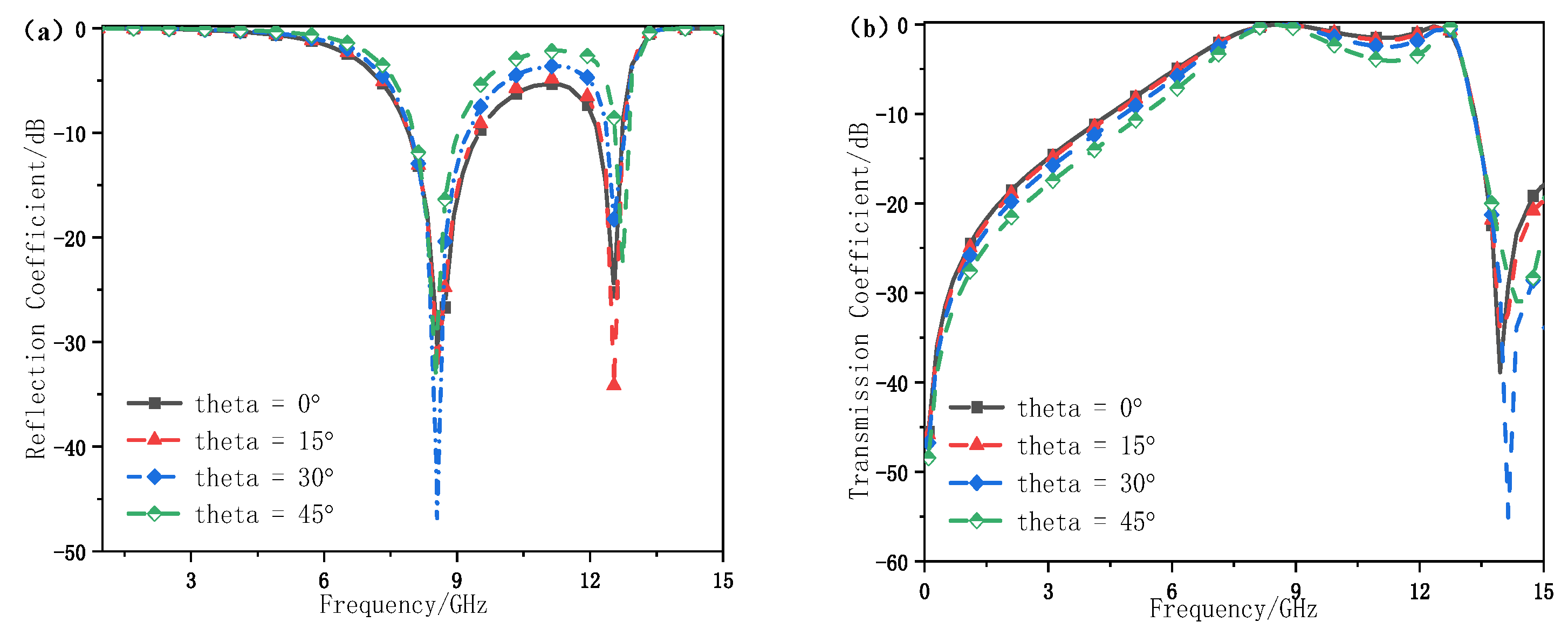
In this paper, numerical calculations were also conducted on the frequency-response curves when different angles were incident on the FSS. The results are shown in Figure 6. In the TE polarization mode, as the incident angle increases, a certain shift occurs at the high-frequency cut-off point. However, overall, this broadband FSS structure still maintains good angular stability within the range of 0° to 45°.
Figure 6a illustrates the reflection coefficient characteristics under varying incidence angles (θ). The low-pass resonant frequency remains stable without observable shift as θ increases from 0° to 45° in 15° increments. In contrast, the high-pass resonant frequency exhibits a noticeable shift of 0.2 GHz toward higher frequencies at θ = 45°, accompanied by a bandwidth reduction of 0.2 GHz for every 15° increase in incidence angle. As shown in Figure 6b, the stopband resonant frequency remains constant at θ ≤ 15°, but shifts progressively by 0.2 GHz toward higher frequencies with each subsequent 15° increment in θ.

2.4. Experimental Testing and Data Analysis

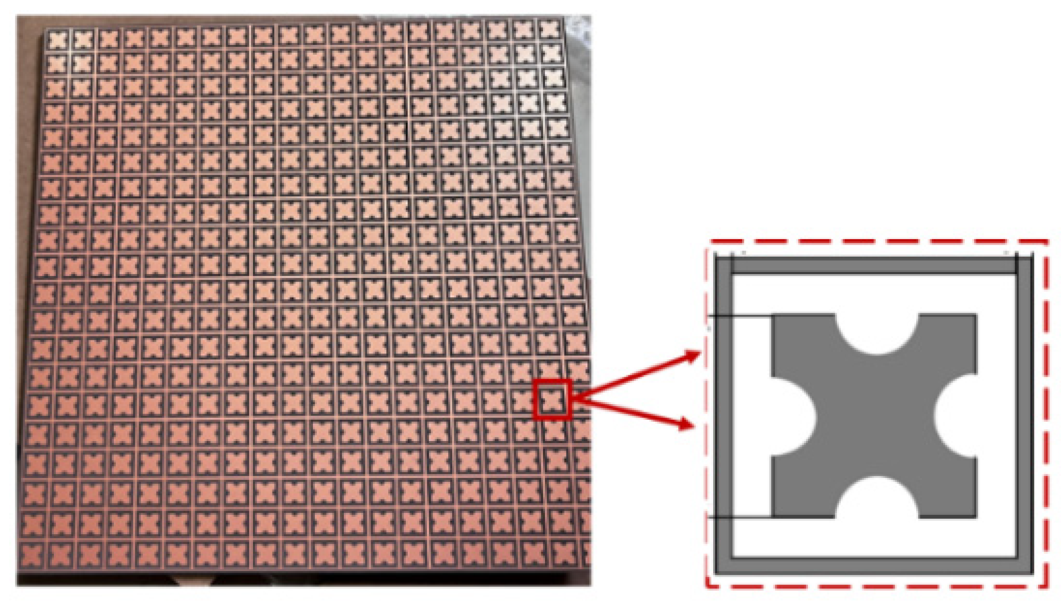
This FSS sample adopts the precision etching process. The processing model and dimensions are completely in accordance with the size parameters in Table 1. The processed sample is shown in Figure 7. The physical size of the entire sample is 202 mm × 202 mm, and the medium plate is made of TLY-5 material.
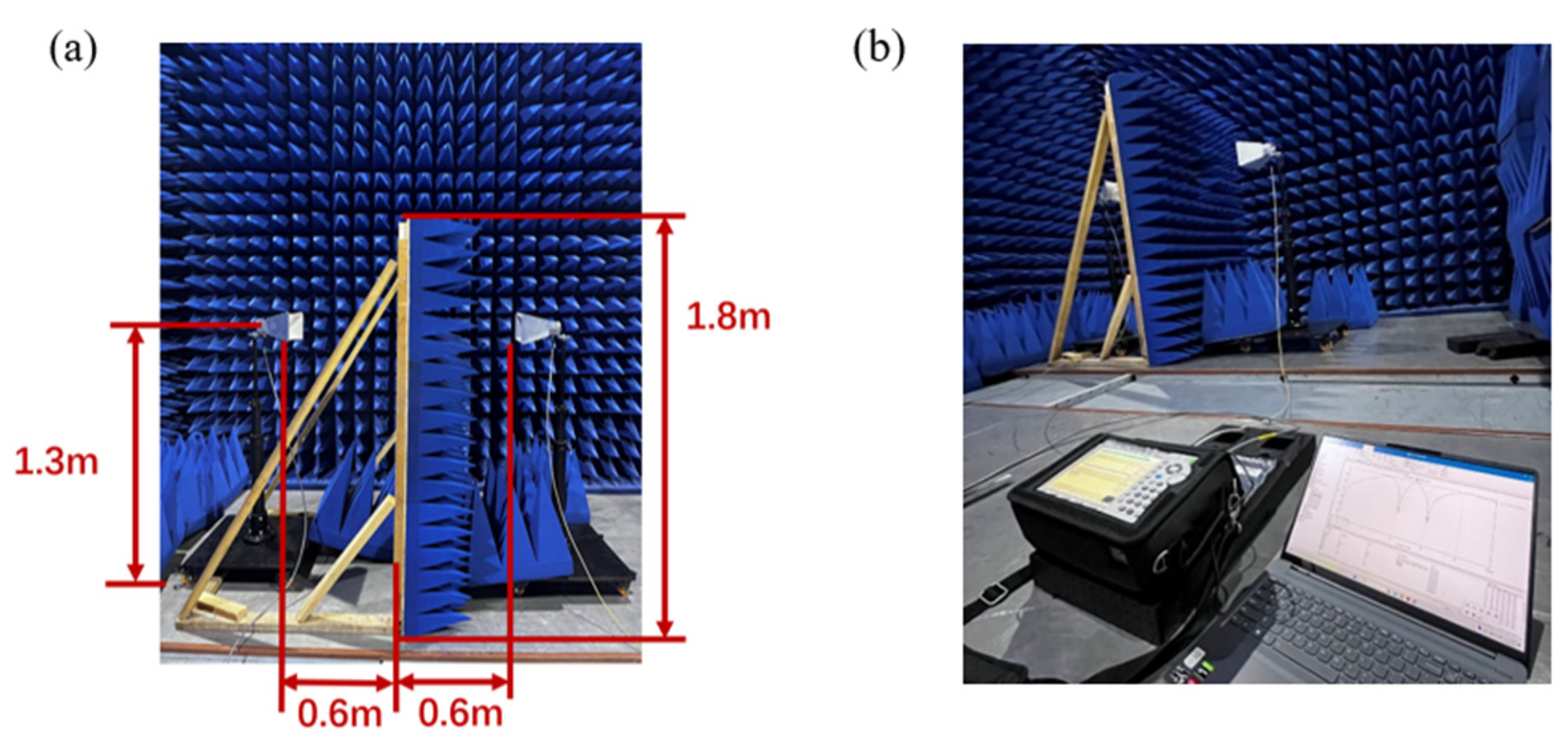
The entire experimental test was carried out in a microwave anechoic chamber, and the free-space method was selected for the test (Figure 8). The operating frequency band of the horn antenna is 1–18 GHZ. The two ports of the vector net meter are, respectively, connected to the transmitting antenna and the receiving antenna. Preheating and equipment calibration are required before each test.
After calibration, the test piece was placed for testing. Figure 9 shows the comparison between the measured results and the simulation results when the electromagnetic wave is vertically incident in the TE polarization mode. At the reflection curve, the measured amplitude at 8.5 GHz is −41.2 dB, and the insertion loss during simulation is −30.5 dB. At the wideband depression (11.1 GHz), the amplitude of the reflection coefficient curve in simulation calculation is −5.4 dB, while the actual test shows −9.8 dB. The measured insertion loss is less than that during simulation. There is no significant deviation between the passband width and the resonant center frequency, and the results are basically consistent.
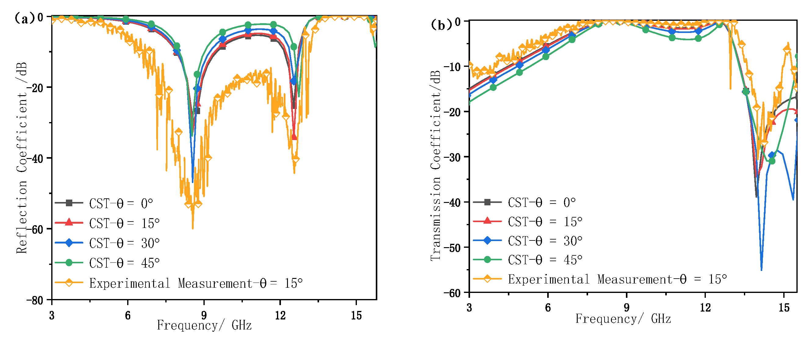
The FSS performance test was also conducted on the sample when electromagnetic waves were incident at an angle. Due to the limited conditions in the actual test, it was impossible to precisely rotate the turntable that fixed the sample to be tested at an angle. Therefore, we only tested the case when the incident angle was 15°. Figure 10 shows the comparison of the actual test and simulation results of the reflection coefficient and transmission coefficient curves in the TE polarization mode.
It can be seen that the resonant frequency points of the reflection coefficient and transmission coefficient curves hardly shift. The 15° oblique incident is in good agreement with the simulation results. However, stray waves occur in the higher frequency band of 12.9 GHz. In the actual test, the amplitude at the passband decreases by about −10 dB on average, and the insertion loss is significantly less than the simulation results.
An analysis of the discrepancy in insertion loss and reflection coefficient reveals the following: under ideal conditions, the FSS model assumes no material loss, perfect structural symmetry, and no additional energy dissipation. When impedance is fully matched, the relationship between the transmission coefficient (|S21|) and reflection coefficient (|S11|) satisfies |S21|2 + |S11|2 = 1, where the squared magnitudes represent transmittance and reflectance, respectively. In simulations, electromagnetic energy is either entirely transmitted or reflected. In practical measurements, however, energy is dissipated through radiation in free space and absorption by surrounding materials, resulting in |S21|2 + |S11|2 < 1. Consequently, the reflection coefficient derived from transmission measurements in real-world environments is necessarily lower than that in ideal simulation conditions.
In a testing environment, the propagation loss of electromagnetic waves in air primarily stems from absorption effects due to interactions with oxygen molecules, water vapor, and other atmospheric constituents, as well as scattering effects caused by particulate matter. These effects intensify with increasing frequency and humidity, leading to an exponential decay of electromagnetic wave intensity with propagation distance, governed by the Formula (8), where α denotes the attenuation coefficient.
I = I 0 e α x
Meanwhile, wave-absorbing materials are designed with tailored impedance matching to maximize the penetration of electromagnetic waves into the material. The incident energy is then dissipated through dielectric loss, magnetic loss, and structural dissipation mechanisms, effectively converting electromagnetic energy into heat. This process significantly reduces the intensity of reflected waves—a reflection loss (RL) of ≤−10 dB indicates absorption of 90% of the incident energy. These two mechanisms work synergistically to attenuate electromagnetic energy: atmospheric propagation loss directly weakens the transmitted signal, while wave-absorbing materials minimize secondary reflections and interference through active energy absorption, thereby ensuring measurement accuracy.
In summary, by comparing the transmission curves of the measured results with those of the simulation results, it is found that there is no significant deviation in the passband width and the resonant center frequency, and the error is within a reasonable range. Based on the calculation results of the two numerical simulations of ADS and CST in Figure 5 above, the accuracy of the entire model design was verified. This provides an accurate design basis for the subsequent AFSS active reconfigurable model design.

3. Research on the Structural Model Design and Regulation Mechanism of AFSS

In order to achieve AFSS with band-switching function and frequency-tuning characteristics, it is proposed to adopt the fusion-loading method of switching devices and varactor diodes. In addition, the feeding of diodes is carried out all through the upper and lower layer structure and the metal through holes to form a fusion bias network. A simple metal bias-network model is used to provide feeding for AFSS to achieve bias voltage regulation.

3.1. Resonant Structure Design

Based on the analysis in Section 2.2, the annular structure exhibits favorable polarization and angular stability, along with enhanced suppression of grating lobes. Accordingly, a meandered square-ring structure is introduced. The aperture unit and the central patch form two nested and mutually insulated parts, facilitating independent biasing for active components. The meandering design increases the effective electrical length of both the metal grid and the aperture, thereby significantly enhancing the equivalent inductance and capacitance. Furthermore, this bent topology contributes to miniaturization, which notably improves angular stability under oblique incidence [28].
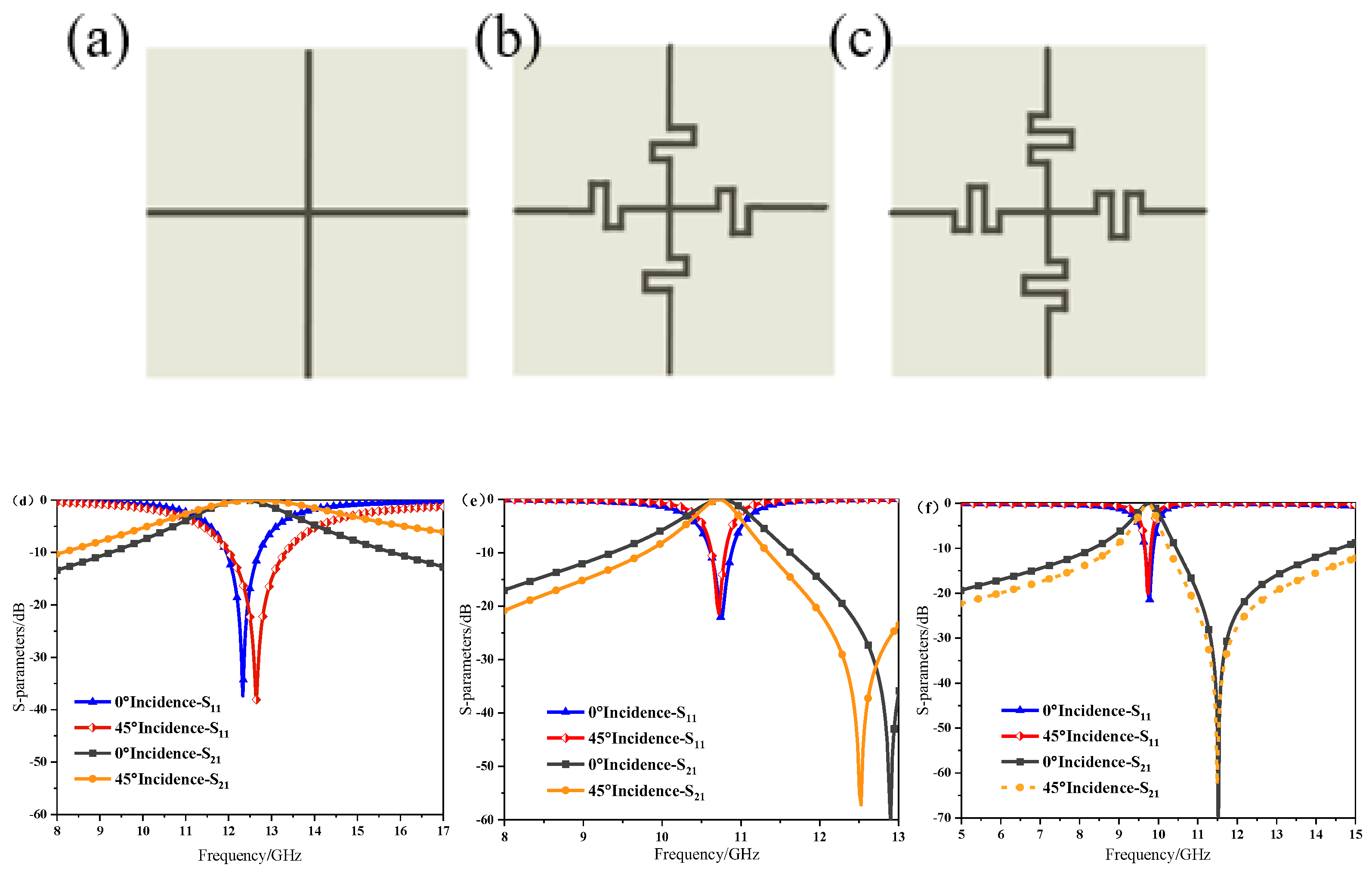
The bias-network design also incorporates a meander-line-based cross-cell structure. Figure 11a–c illustrate the evolution of the bent cross-patch geometry. Simulations were performed on composite FSS configurations consisting of a top-layer ring structure and three variants of bottom-layer cross-patch units. The corresponding S-parameters under various oblique incidence angles are presented in Figure 11d–f.
It can be seen that as the degree of miniaturization increases, the continuous increase in the number of bends causes the resonant frequency to shift towards the low frequency, and the resonant bandwidth gradually narrows. The relative bandwidth of the unbent cross patch is 23.6% (13.8–10.8 GHz), while that of the double-bent cross patch structure drops to 7.4% (11.1–10.3 GHz). After three bends, the relative bandwidth of the cross-shaped patch drops to 6.7% (9.4–10.0 GHz). In the unbent cross structure, a frequency offset of 0.3 GHz occurs when the incident is normal and the incident is oblique at 45°. The frequency hardly shifts during the secondary bending, but the bandwidth decreases when the incident is oblique compared to the normal incident. After three bends, the resonant frequency and working bandwidth of the structure remain almost unchanged when the incident is oblique. This indicates that the more bends are introduced into the branch, the greater the angular stability will be.

3.2. Analysis of Passive Structure Model and Transmission Characteristics

3.2.1. Design of Feeding and Bias Networks

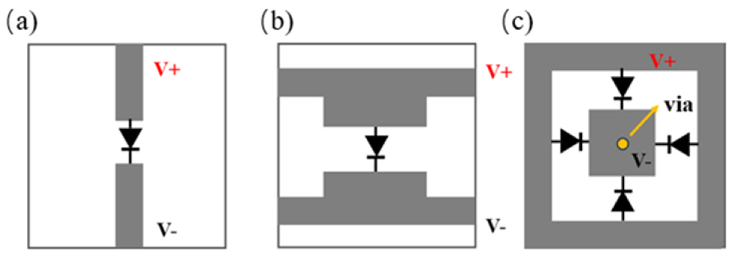
Compared with the passive FSS structure without active components, the diode-loaded reconfigurable AFSS requires additional consideration of the biasing network in the design. As illustrated in Figure 12, commonly used biasing schemes include series biasing networks, parallel-integrated biasing networks, and the incorporation of metallic vias.
Among the various biasing schemes, the approach based on incorporating metallic vias has been extensively investigated. The metallic vias vertically penetrate the entire dielectric layer and connect the top and bottom metallic structures. While extending the effective resonance path, the vias also introduce parasitic capacitance and inductance, which participate in the resonance. From the perspective of the equivalent circuit, the metallic part can be modeled as an inductance Lv, whereas the gap between adjacent vias can be modeled as a capacitance Cv. The increase in equivalent inductance and capacitance further reduces the resonance frequency. The calculation formulas for the equivalent inductance and capacitance are expressed as:
L v = μ 0 π cos h g v i a 2 R v i a h
C v = π ε 0 ε r cos h g v i a 2 R v i a h
Here, h represents the via height, Rvia denotes the cross-sectional radius, and gvia refers to the spacing between adjacent vias. As indicated by the above expressions, the additional inductance and capacitance introduced by the metallic vias can be controlled through careful optimization of their physical dimensions, thereby mitigating their impact on the resonance frequency.
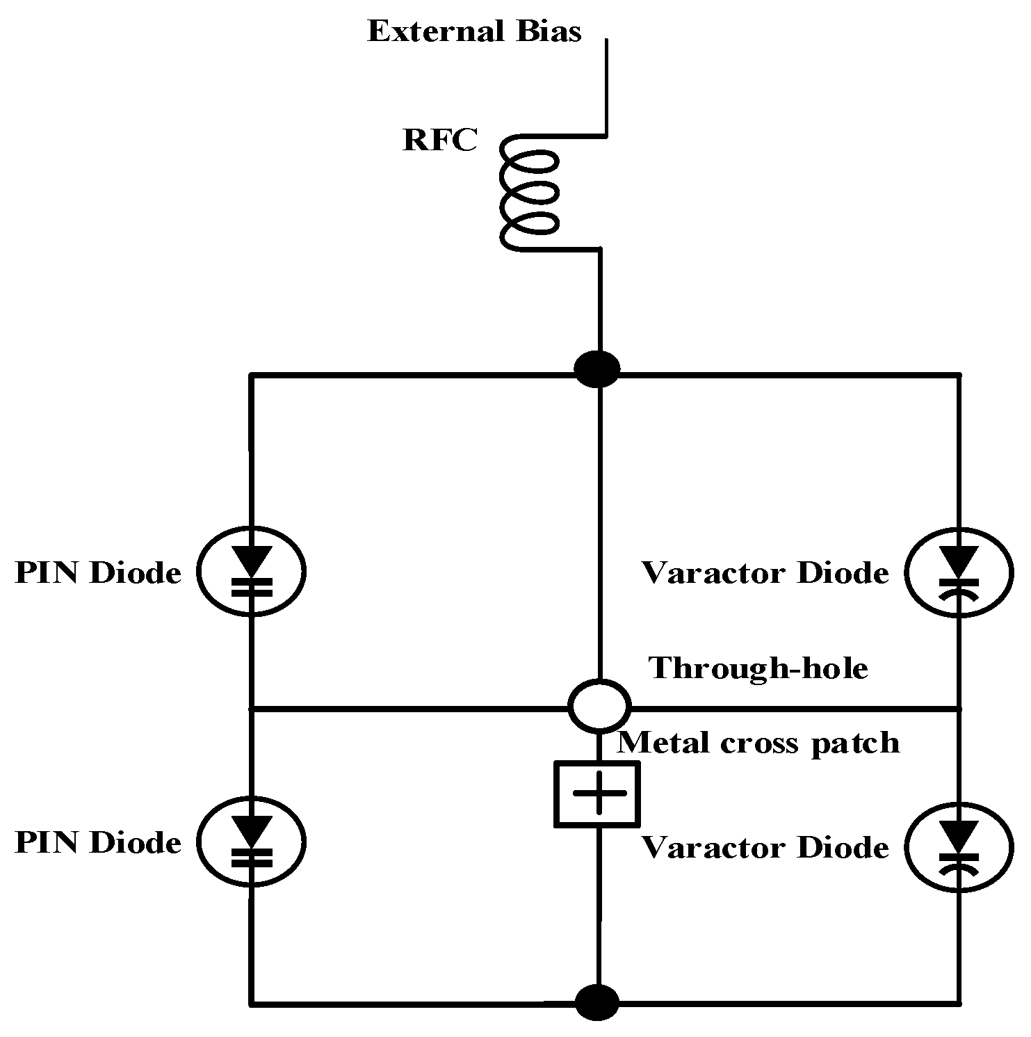
The proposed active structure (Figure 13) employs a feeding scheme in which four diodes (two PIN diodes and two varactor diodes) are symmetrically arranged along the y-axis. The anodes are connected to the metallic region inside the annular aperture, while the cathodes are uniformly connected to the outer conductor to form a closed loop, thereby achieving electromagnetic isolation. The metallic part of the annular aperture serves as an electromagnetic shielding layer, with bent edges to enhance angular stability, effectively isolating the internal circuit from external electromagnetic interference. The cross-shaped patch, implemented as an interlayer structure, reduces electromagnetic coupling from external power supplies or signal sources and suppresses crosstalk; in addition, it is rotated by 45° to facilitate coupling with the internal electromagnetic field. A metallic via is introduced at the center of the unit cell, embedded in the middle layer as the feeding network, to provide bias voltage for the diodes. The metallic via further enables bias connections for power and signal distribution between different circuit layers. By optimizing the design of the outer conductor, metallic vias, and ground loop, the isolation between RF signals and the bias network can be significantly improved, parasitic coupling and signal interference can be suppressed, and the electromagnetic compatibility and overall performance of the system are consequently enhanced.

3.2.2. Structural Model Design

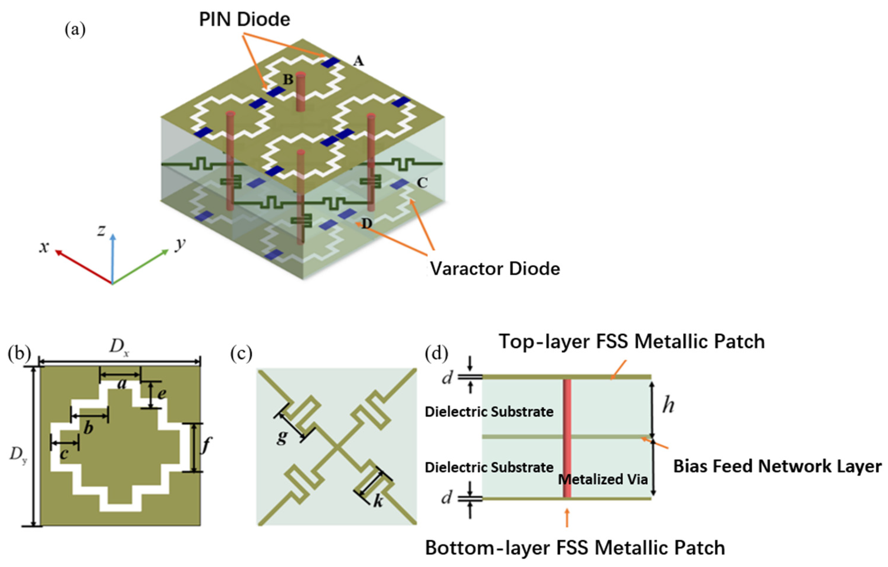
After completing the design optimization, the AFSS structure model of the fusion loading diode proposed in this project is shown in Figure 14a. The overall model consists of three metal layers and two dielectric substrates spaced apart. The top and bottom metal layers are made of traditional square-ring hole diameter structures that have been deformed and have exactly the same structural dimensions. The middle power-supply layer is a tortuous structure formed by bending a traditional cross patch with branches to enhance the angular stability of the overall structure. The medium material selected is Rogers 5880 (The manufacturer of Rogers 5880 is Rogers Corporation. Rogers Corporation is headquartered in Chandler, AZ, USA, and its country of origin is the United States). Metal is fed through holes that run through the entire structure for convenient power supply. The other parameters of the structure are shown in Table 2.
To validate the correctness of the proposed model, this study employs two full-wave electromagnetic simulation tools, HFSS and CST, to construct the models separately and performs simulation analysis under TE polarization with normal incidence. The S-parameter results obtained from both software packages, as depicted in Figure 15, consistently indicate a distinct band-pass resonance at 12.2 GHz and a −3 dB operating bandwidth of 1.8 GHz (covering 11.4 GHz to 13.2 GHz). The high agreement between the simulation results effectively verifies the accuracy and reliability of the proposed model.
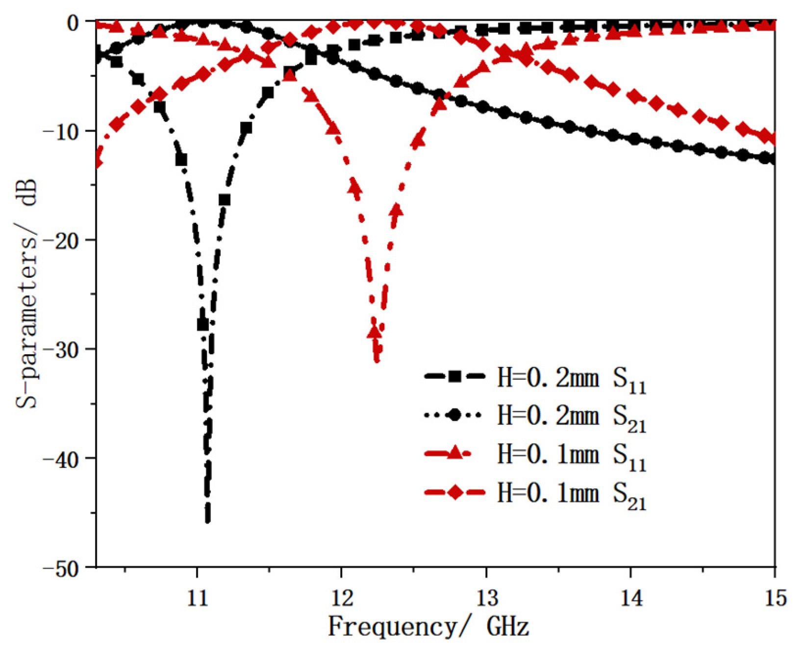
The insertion loss introduced by the dielectric substrate cannot be neglected. We investigated the effect of the thickness of the dielectric substrate. Figure 16 shows the frequency-response curve when the thickness h of the two dielectric layers increases to 0.2 mm. For a double-side dielectric-loaded FSS, the operating frequency is calculated by the formula f = f 0 / ε r . Consequently, as the thickness of the dielectric substrate increases, its resonant frequency decreases. The increased thickness leads to a narrower bandwidth, with the −3 dB bandwidth reduced to 1.5 GHz (10.3–11.8 GHz). This is attributed to the reduced coupling effect between the upper and lower layered structures caused by the greater thickness, which prevents the bandwidth from being broadened. To mitigate this issue, employing substrate materials with a lower dielectric constant or reduced loss tangent, alongside optimizing the metallic pattern layout to enhance interlayer coupling, could be promising strategies for improving bandwidth performance without substantially increasing the overall thickness.
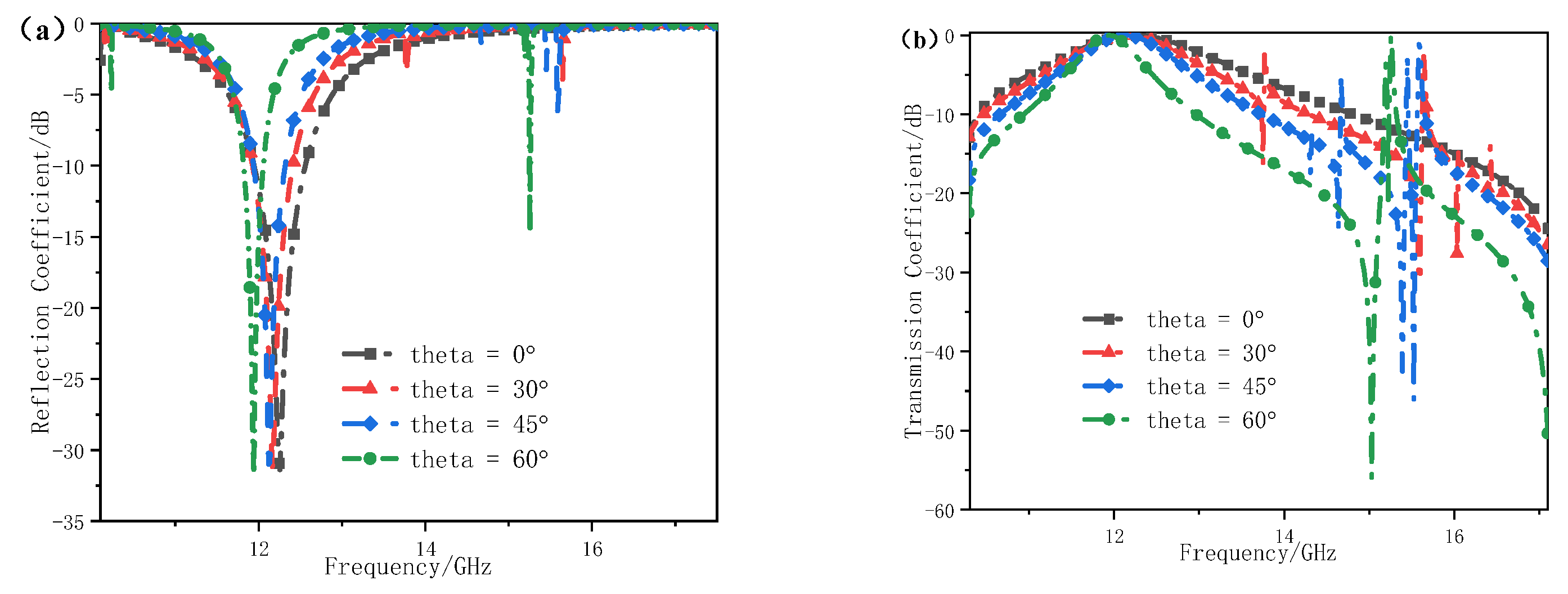
The angular stability of the structure was systematically evaluated under oblique incidence. As shown in Figure 17, under transverse electric (TE) polarization, the resonant frequency remains highly consistent with increasing incidence angle: it shifts only from 12.25 GHz to 12.16 GHz at 15°, and to 12.13 GHz at 30°, resulting in a negligible cumulative deviation of approximately 0.12 GHz within 0–30°. This indicates excellent angular stability, which is highly desirable for frequency-selective surfaces (FSS) or absorbers requiring consistent performance across a wide angular range. Meanwhile, the −3 dB bandwidth decreases from 1.8 GHz (11.4–13.2 GHz) to 1.5 GHz (11.4–12.9 GHz) and further to 1.1 GHz (11.5–12.6 GHz), respectively.
Although higher-order resonances emerge at elevated frequencies with increasing angles, the operating frequency remains virtually unaffected, and favorable bandpass characteristics are retained within the principal operating band. This robust performance can be attributed to the low profile of the structure and the miniaturized bent geometry, which collectively suppress sensitivity to angle variations.
When the oblique incident angle θ increases from 0° to 60°, the resonant frequency slightly shifts to the low frequency by 0.4 GHz, and the bandwidth at −3 dB decreases from 1.8 GHZ to 0.7 GHz (11.6–12.3 GHz). However, the out-of-band suppression characteristics deteriorate at this time. The reason for this is that the cascading of multi-layer FSS will introduce interlayer electromagnetic coupling. When incident at an angle, the resonant units of different layers will have different phase delays of the incident wave. For high-order resonant waves above 16 GHz, according to the critical conditions for the occurrence of the gate-flap phenomenon, they may be partially satisfied d s i n θ λ / 2 , when incident at an angle of 60°. When incident at a large angle of 60°, the gate-flap phenomenon will introduce additional resonant modes at high-frequency points.
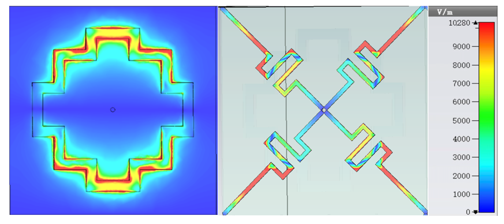
In addition, the electric-field intensity distribution map of the AFSS structure at the resonant frequency of 12.2 GHz is also provided. As shown in Figure 18, the strong field area is concentrated at the bent aperture and the metal arm of the cross-shaped patch. This indicates that the obvious resonance phenomenon of FSS at this location is caused by the strong coupling resonance between the upper and lower annular aperture and the metal branch in the middle layer.

3.2.3. Equivalent Circuit Analysis of Passive Structures

The equivalent circuit method is adopted to deeply analyze the working principle of AFSS. As shown in Figure 19, it is the equivalent circuit model of AFSS without loading diodes. The metal patches of the top and bottom structures are equivalent to LC parallel resonant circuits, where L1 and L2 are the equivalent inductance of the top and bottom metal patches, and C1 and C2 are the equivalent capacitance of the bent annular groove as a whole. The metal-band grid and metal through holes in the middle layer are equivalent to parallel Lthrough hole modeling.
The two-layer dielectric substrate can be equivalent to a transmission line of length h and characteristic impedance Z T = Z 0 / ε r , and the transmission line can be modeled by an equivalent circuit of series inductance L h = μ 0 μ r h and parallel capacitance C h = ε 0 ε r h / 2 . The free space on both sides of the FSS is equivalent to a transmission line with characteristic impedance Z0 = 377 Ω. As described in Figure 2 above, this equivalent circuit model can also be regarded as a second-order coupled resonant bandpass filter [16].
Figure 20a presents a simplified model of the above-mentioned equivalent circuit model and further models it in ADS. Figure 20b shows a comparison of the reflection coefficient curves obtained by the ADS equivalent circuit without a diode structure and the CST simulation. The equivalent circuit structure is in good agreement with the numerical simulation results, with only slight offsets in the operating frequency and bandwidth.

3.3. Design of Active Structure Model for Loading PIN/Varactor Diode

3.3.1. Analysis of the Transmission Characteristics of Loaded PIN Diodes

Numerical simulations were conducted to evaluate the performance of the switchable AFSS loaded with PIN diodes. As depicted in Figure 14a, two PIN diodes are integrated at points A and B. In the simulation, the diodes are modeled as ideal switches: when turned ON, they are represented as small resistors; when OFF, they are approximated as capacitors. The internal resistance of the diodes was neglected in this model.
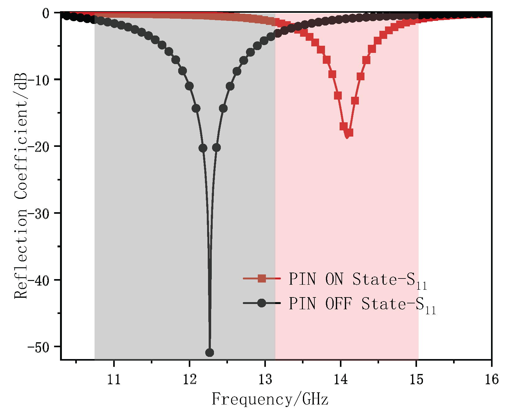
Figure 21 presents the reflection coefficient curve of the FSS of the PIN diode in the ON/OFF state under TE polarization. When the PIN diode is in the cut-off state, the resonant point within this passband is located in the X-band, with a resonant frequency of 12.2 GHz and a relative bandwidth of −3 dB of 14.8%. When on, a new resonant frequency appears at 14.1 GHz, and the insertion loss increases to −20 dB. It exhibits stopband characteristics within the original passband range of 10.5 GHz to 13.1 GHz. The above achieves the switching of the operating frequency between different bands of the AFSS under different bias states of the PIN diode.

3.3.2. Analysis of the Transmission Characteristics of Loaded Varactor Diodes

Based on the structure with a PIN diode loaded at the top layer, a varactor diode is loaded at the bottom layer. The loading positions are shown in Figure 14a in the previous text. Figure 19 shows the reflection coefficient curve of the AFSS structure with both a PIN and a varactor diode loaded simultaneously under TE polarization.
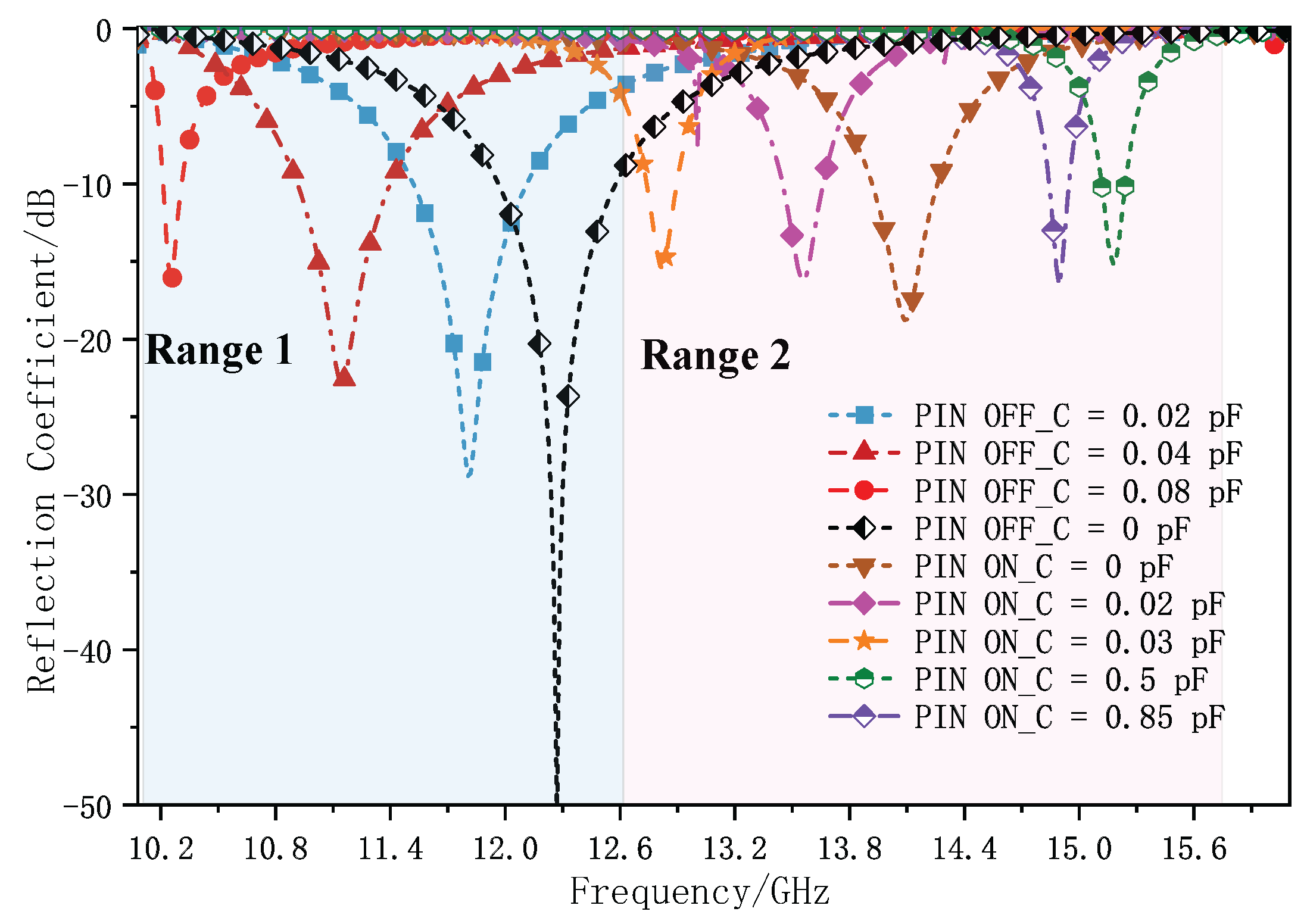
Under normal electromagnetic wave incidence, the AFSS exhibits a center frequency of 12.3 GHz and a −3 dB bandwidth of 1.8 GHz (11.4–13.2 GHz) in the PIN-OFF state (Figure 22). When the PIN diode is reverse-biased, and additional capacitances of C = 0.02 pF, 0.04 pF, and 0.08 pF are applied to the varactor diode, the passband shifts progressively toward lower frequencies as the capacitance increases, accompanied by a reduction in bandwidth. At C = 0.08 pF, the operating frequency decreases to 10.2 GHz. Moreover, the insertion loss within the passband ranges from −50 dB to −15 dB, indicating that the incorporation of multiple PIN and varactor diodes introduces significant insertion loss.
When the PIN diode is forward-conducting and no additional capacitance is applied to the varactor, a new transmission band emerges at 14.1 GHz. Loading the varactor with small capacitances (C = 0.02 pF and 0.03 pF) further reduces the resonant frequency to 12.8 GHz. Accordingly, the −3 dB bandwidth narrows from 1.1 GHz (13.5–14.6 GHz) to 0.6 GHz (12.5–13.1 GHz), while the insertion loss increases from −19 dB to −15 dB. Under forward bias and with larger varactor capacitances (C = 0.5 pF and 0.85 pF), the operating frequency shifts upward to 15.2 GHz, though with increased insertion loss of −15 dB.
To sum up, by loading two pins and varactor diodes on the top and bottom layers of the AFSS unit, respectively, the wide-range tunable frequency-response characteristics of the AFSS can be achieved by applying different bias voltages. Range 1 (10.1–12.2 GHz) is located in the X band. Range 2 (12.2–15.6 GHz) is located in the Ku band. The frequency ranges of the two bandpass modes of AFSS are interconnected, transiting between adjacent frequency bands to cover the entire spectrum, and the comprehensive tuning range is expanded to 10.1–15.6 GHz.
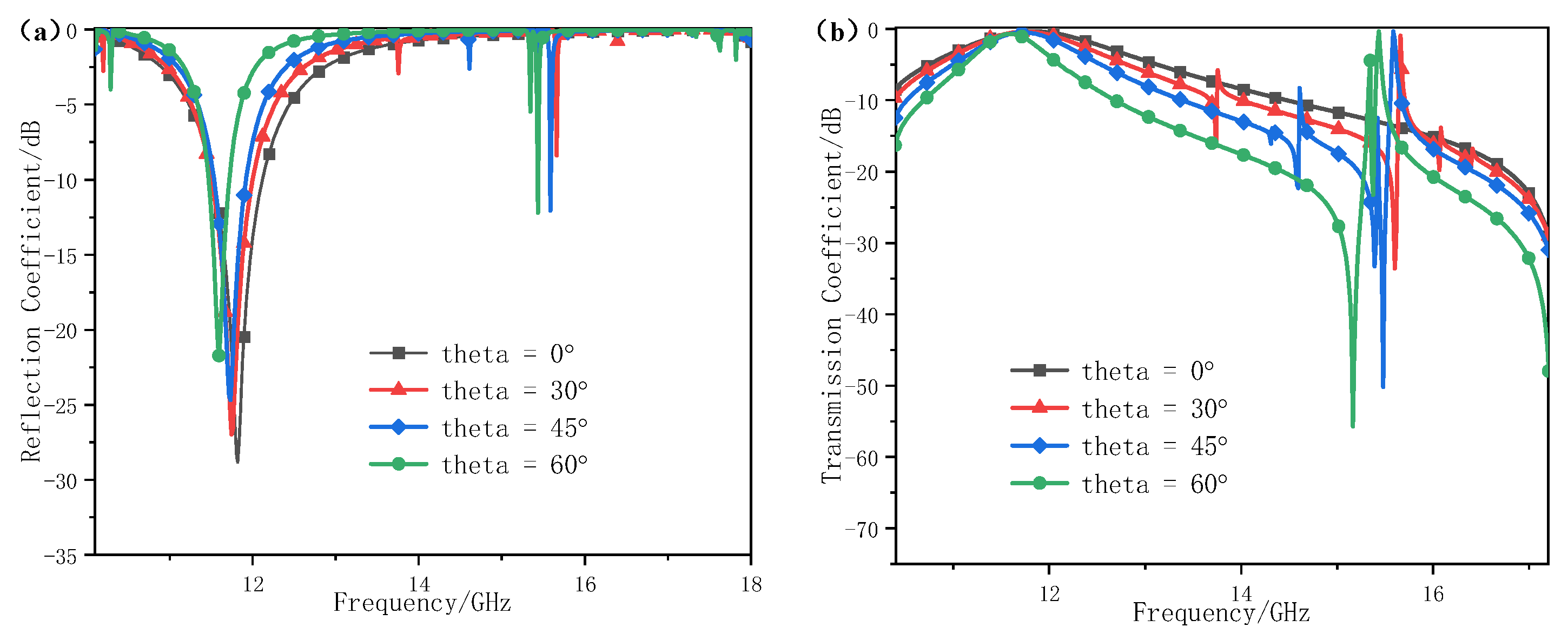
The angular stability of the proposed AFSS under oblique incidence was also investigated. The designed active frequency-selective surface exhibits excellent angular stability in the PIN-OFF state. As illustrated in Figure 23, the transmission response remains highly consistent across incidence angles from 0° to 45°: the resonant frequency shifts only slightly from 11.82 GHz to 11.74 GHz as the angle increases from 0° to 30°, and remains stable at 11.71 GHz between 30° and 45°. Even at an extreme angle of 60°, the center frequency deviates by only 0.1 GHz, demonstrating remarkable angular stability over a wide angular range—a critical feature for applications requiring consistent performance under varying illumination conditions.
As the angle of incidence increases to 60°, higher-order harmonics emerge at high frequencies, and weak out-of-band resonances become observable. This phenomenon may be attributed to the coupling between the vertical component of the electric field and the metalized vias, which excites parasitic resonances. Nevertheless, these parasitic resonances in the stopband do not compromise the bandpass characteristics. The structure maintains a well-defined −3 dB transmission band in the principal passband (10.9–12.8 GHz). Thus, the proposed wide-range frequency-tunable AFSS achieves favorable angular stability even under large-angle oblique incidence.
Table 3 presents a comprehensive comparison between the proposed active frequency-selective surface (FSS) model integrating both PIN and varactor diodes, and existing structures that utilize only varactor diodes for tuning. The results demonstrate that by combining PIN and varactor diodes in a coordinated tuning mechanism, the proposed architecture achieves broad frequency-tuning range while maintaining excellent angular stability, exhibiting superior overall performance compared to structures relying solely on a single tuning method.

3.3.3. Equivalent Circuit Analysis of Integrated PIN/Varactor Diodes Loading

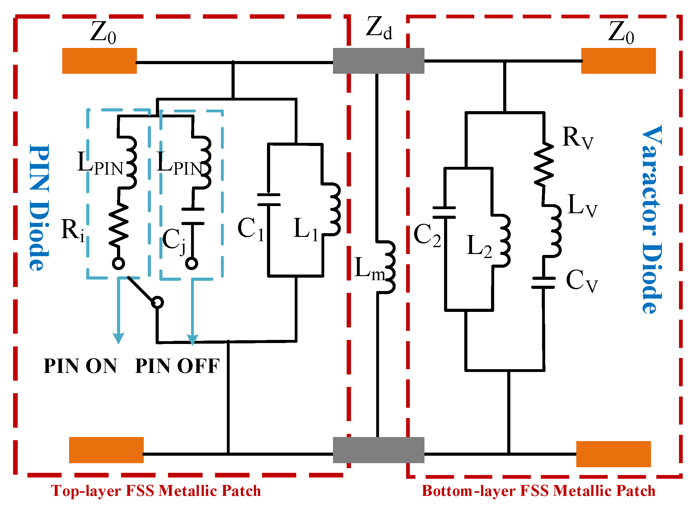
The frequency reconfigurable characteristics of AFSS are analyzed by using the equivalent circuit method (Figure 24). In the equivalent circuit, the inductance mainly comes from the metal structure, and the aperture gap is equivalent to a capacitor. When a PIN diode is forward-biased, it can be equivalent to a small on-resistance, which is like grafting a wire connecting the external metal and the internal metal onto a bent annular groove. At this time, the metal patch presents a total reflection state. When the PIN diode is reverse-biased, it can be equivalent to the capacitance Cj. At this time, the annular slot is in an open circuit state, and the filter response remains unchanged. The equivalent parameters Rv, Lv and Cv of the varactor diode are added in series to the equivalent circuit, and Zd is the characteristic impedance of the transmission line.
From the analysis of the equivalent circuit model, the process of achieving continuous tuning of the operating frequency band over a wide frequency range by the above-mentioned composite regulating diode is essentially a process of dynamically changing the equivalent inductance and capacitance values of the LC parallel resonant circuit to alter the resonant frequency point. This method can flexibly adjust the resonant frequency according to actual needs and effectively expand the range of resonant frequency adjustment [30].

4. Conclusions

This paper presents a reconfigurable active frequency-selective surface (AFSS) structure co-loaded with PIN and varactor diodes. The design incorporates an integrated bias network architecture, enabling both multi-band switching and wide-range continuous frequency tuning. It provides an innovative solution for adaptive spectrum control and stealth applications in complex electromagnetic environments.
During the initial design phase, the validity of the unit-cell model based on equivalent circuit theory was verified through full-wave simulations and experimental measurements. This approach established a theoretical foundation for system-level AFSS modeling and feed network design. The integrated bias network not only meets the multi-voltage requirements of the hybrid diodes but also minimizes parasitic coupling effects from bias lines on transmission response. Furthermore, meandered metal-patch topology optimization was introduced to enhance phase stability under oblique incidence, improving adaptability in practical engineering scenarios. Experimental results show that toggling the PIN diodes (ON/OFF) enables dynamic switching between the X-band (8–12 GHz) and Ku-band (12–18 GHz). This functionality allows the structure to serve as a smart radome or frequency-selective reflector in satellite communication and radar systems, supporting multi-band multiplexing and reconfiguration to improve spectrum utilization and integration level. Continuous tuning of the varactor diode bias voltage achieves broadband frequency agility from 10.2 GHz to 15.2 GHz, with an insertion loss below −1 dB. Theoretical analysis based on equivalent circuit models and electric-field distributions clarifies the electromagnetic modulation mechanisms under multi-mode operation, confirming the value of the equivalent circuit method for guiding active metasurface design. Future work may extend such co-design strategies to terahertz frequencies by leveraging concepts from graphene-based terahertz AFSS, opening new possibilities for 6G communications and high-resolution imaging. However, the hybrid integration of PIN and varactor diodes in this design still faces challenges such as bias network complexity, intricate fabrication, and higher system cost. These issues remain critical for future engineering-oriented AFSS development.

Author Contributions

Conceptualization, X.L. and S.S.; Methodology, G.Z. and S.S.; Software, X.T. and G.Z.; Validation, H.L.; Investigation, X.L. and J.S.; Data curation, X.T.; Writing—original draft, L.G.; Writing—review & editing, L.G.; Supervision, L.W.; Funding acquisition, Z.Y. and L.G. All authors have read and agreed to the published version of the manuscript.

Funding

National Natural Science Foundation of China (62201566); Natural Science Foundation of Shaanxi Province (2025JC-YBMS-744); The Youth Innovation Team of Shaanxi Universities (K20220184).

Data Availability Statement

Data underlying the results presented in this paper are not publicly available at this time but may be obtained from the authors upon reasonable request.

Acknowledgments

The authors sincerely appreciate all financial and technical support.

Conflicts of Interest

The authors declare no conflicts of interest.

References

  1. Xie, J. Research on Low-Profile High-Order Bandpass Frequency Selective Surfaces. Ph.D. Thesis, Nanjing University of Posts and Telecommunications, Nanjing, China, 2022. (In Chinese). [Google Scholar]
  2. Deng, B. Research on the Application of Metamaterials in Active Frequency Selective Surfaces. Master’s Thesis, Chengdu University of Information Technology, Chengdu, China, 2018. (In Chinese). [Google Scholar]
  3. Sainadh, P.M.; Ghosh, S. A Multifunctional Reconfigurable Frequency-Selective Surface with Simultaneous Switching and Tuning Capability. IEEE Trans. Antennas Propag. 2024, 72, 7700–7709. [Google Scholar] [CrossRef]
  4. Han, J.; Liao, X. A MEMS Microwave Phase Detector with Broadband Performance Operable at X-Band. Microw. Opt. Technol. Lett. 2016, 58, 806–809. [Google Scholar] [CrossRef]
  5. Schoenlinner, B.; Abbaspour-Tamijani, A.; Kempel, L.C.; Rebeiz, G. Switchable Low-Loss RF MEMS Ka-Band Frequency-Selective Surface. IEEE Trans. Microw. Theory Tech. 2004, 52, 2474–2481. [Google Scholar] [CrossRef]
  6. Zhang, D.; Zhang, L. Tunable Terahertz Dual-Band Band-Stop Filter Based on Surface Magnetoplasmons in Graphene Sheet Array. Opt. Laser Technol. 2020, 132, 106484. [Google Scholar] [CrossRef]
  7. Xu, Y.; Gao, J.; Xu, N. Low-Frequency Bandpass and Bandstop Free-Switching Frequency Selective Surface. Opt. Precis. Eng. 2018, 26, 142–149. (In Chinese) [Google Scholar]
  8. Yang, C. Analysis and Design of Bandpass Reconfigurable Frequency Selective Surfaces. Master’s Thesis, Xidian University, Xi’an, China, 2023. (In Chinese). [Google Scholar]
  9. Zheng, H.; Zhang, S.; Xu, T. Research Progress on Tunable Electromagnetic Metasurfaces. Acta Opt. Sin. 2023, 43, 55–75. (In Chinese) [Google Scholar]
  10. Kiani, G.I.; Esselle, K.P.; Weily, A.R.; Ford, K.L. Active Frequency Selective Surface Using PIN Diodes. In Proceedings of the Antennas and Propagation Society International Symposium, Honolulu, HI, USA, 9–15 June 2007; pp. 1–4. [Google Scholar]
  11. Withayachumnankul, W.; Fumeaux, C.; Abbott, D. Planar Array of Electric-LC Resonators with Broadband Tunability. IEEE Antennas Wirel. Propag. Lett. 2011, 10, 577–580. [Google Scholar] [CrossRef]
  12. Ebrahimi, A.; Shen, Z.; Withayachumnankul, W.; Al-Sarawi, S.F.; Abbott, D. Varactor-Tunable Second-Order Bandpass Frequency-Selective Surface with Embedded Bias Network. IEEE Trans. Antennas Propag. 2016, 64, 1672–1680. [Google Scholar] [CrossRef]
  13. Phon, R.; Ghosh, S.; Lim, S. Novel Multifunctional Reconfigurable Active Frequency Selective Surface. IEEE Trans. Antennas Propag. 2019, 67, 1709–1718. [Google Scholar] [CrossRef]
  14. Li, H.; Cao, Q.; Wang, Y. A Multifunctional Active Frequency Selective Surface and Its Control Method. Chinese Patent CN201610852810.9, 11 October 2019. (In Chinese). [Google Scholar]
  15. Bai, H.; Yan, M.; Li, W.; Wang, J.; Zheng, L.; Wang, H.; Qu, S. Tunable Frequency Selective Surface with Angular Stability. IEEE Antennas Wirel. Propag. Lett. 2021, 20, 1108–1112. [Google Scholar] [CrossRef]
  16. He, Z. Research on Miniaturized Multi-Frequency Reconfigurable Frequency Selective Surfaces. Master’s Thesis, Chongqing University of Posts and Telecommunications, Chongqing, China, 2022. (In Chinese). [Google Scholar]
  17. Li, H.; Ma, C.; Zhou, T.; Wang, J.; Ye, D.; Sun, Y.; Zhu, W.; Denidni, T.A.; Ran, L. Reconfigurable Fresnel Lens Based on an Active Second-Order Bandpass Frequency-Selective Surface. IEEE Trans. Antennas Propag. 2020, 68, 4054–4059. [Google Scholar] [CrossRef]
  18. Shao, W.; Ding, X.; Zhang, L.M. A Multifunctional Active Frequency Selective Surface with Scattering Diffusivity and Transmission Passband Tunability. IEEE Antennas Wirel. Propag. Lett. 2024, 23, 229–233. [Google Scholar]
  19. Qu, M.; He, Z.; Su, J.; Nayyeri, V. A rasorber with energy-selective passband and ultrawideband absorptiveout-of-band. IEEE Trans. Microw. Theory Tech. 2024, 72, 5643–5652. [Google Scholar] [CrossRef]
  20. Wang, H.; Liu, N.; Sheng, X. A Dual-Band Reconfigurable Frequency Selective Surface with Independent Tuning Capability. IEEE Antennas Wirel. Propag. Lett. 2024, 23, 3917–3921. [Google Scholar] [CrossRef]
  21. Fan, Y.D.; Li, D.; Ma, H.Z.; Li, E.-P. A Novel Reconfigurable Metasurface with Expanded Tuning Range for Electromagnetic Interference Shielding. In Proceedings of the 2024 IEEE Joint International Symposium on Electromagnetic Compatibility, Signal & Power Integrity: EMC Japan/Asia-Pacific International Symposium on Electromagnetic Compatibility, Okinawa, Japan, 20–24 May 2024; pp. 505–510. [Google Scholar]
  22. Chen, B. Design of Miniaturized Frequency Selective Surfaces Based on Equivalent Circuit Analysis. Fire Control Radar Technol. 2018, 47, 85–93. (In Chinese) [Google Scholar]
  23. Liang, J. Research and Design of Flexible, Wideband, and Tunable Multifunctional Active Frequency Selective Surfaces. Ph.D. Thesis, Nanjing University of Aeronautics and Astronautics, Nanjing, China, 2021. (In Chinese). [Google Scholar]
  24. Langley, R.J.; Parker, E.A. Equivalent Circuit Model for Arrays of Square Loops. Electron. Lett. 1982, 18, 294–296. [Google Scholar] [CrossRef]
  25. Maity, S.; Tewary, T.; Mukherjee, S.; Roy, A.; Sarkar, P.P.; Bhunia, S. Wideband Hybrid Microstrip Patch Antenna and Gain Improvement Using Frequency Selective Surface. Int. J. Commun. Syst. 2022, 35, e5268. [Google Scholar] [CrossRef]
  26. Wang, L.; Zhang, Y.; Yang, H. Design of a Novel Miniaturized Stopband FSS for Ultra-Wideband Antennas. J. Magn. Mater. Devices 2019, 50, 50–56. (In Chinese) [Google Scholar] [CrossRef]
  27. Zhang, Y. Research on Novel Wideband and Multi-Band Three-Dimensional Frequency Selective Surfaces. Ph.D. Thesis, Nanjing University of Posts and Telecommunications, Nanjing, China, 2019. (In Chinese). [Google Scholar]
  28. Yao, Z. Design and Research of Miniaturized Frequency Selective Surfaces in the Microwave Band. Master’s Thesis, Jilin University, Changchun, China, 2024. (In Chinese). [Google Scholar]
  29. Ebrahimi, A.; Withayachumnankul, W.; Al-Sarawi, S.F.; Abbott, D. Higher-Order Tunable Frequency Selective Surface with Miniaturized Elements. In Proceedings of the 2016 IEEE MTT-S International Microwave Symposium (IMS), San Francisco, CA, USA, 22–27 May 2016; IEEE: Piscataway, NJ, USA, 2016. [Google Scholar]
  30. Wang, S.; Hong, T. Design of an Active Frequency Selective Surface with Wide Tuning Range. In Proceedings of the 2023 National Conference on Antennas, Nanjing, China, 19–21 October 2023; pp. 865–867. (In Chinese). [Google Scholar]
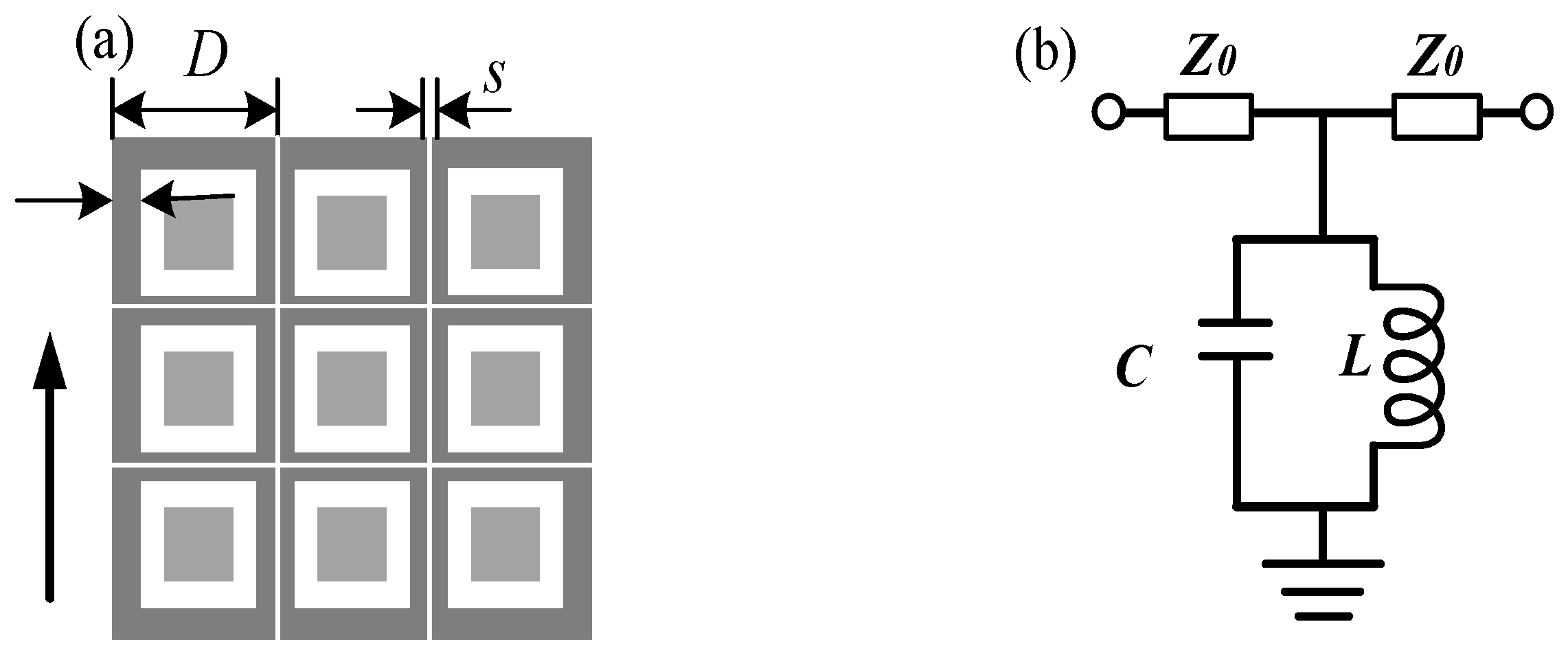
Figure 1. Square-ring aperture structure and its equivalent circuit diagram (a) Schematic diagram of the square-ring aperture structure (b) Equivalent circuit diagram.
Electronics 14 03628 g001
Figure 2. Equivalent circuit model of second-order filtering structure.
Electronics 14 03628 g002
Figure 3. Model of FSS ring structure with wideband characteristics: (a) structural diagram; (b) overall structural cross-section.
Electronics 14 03628 g003
Figure 4. Frequency response characteristics of broadband FSS.
Electronics 14 03628 g004
Figure 5. Comparison chart of S11 curves simulated by CST/ADS.
Electronics 14 03628 g005
Figure 6. Frequency-response characteristic curve at an incident angle of 0–45° in TE polarization mode: (a) reflection coefficient S11; (b) transmission coefficient S21.
Electronics 14 03628 g006
Figure 7. A photo of broadband-ring FSS.
Electronics 14 03628 g007
Figure 8. Test system setup environment: (a) physical picture of the test device; (b) physical connection picture of the arrow net instrument.
Electronics 14 03628 g008
Figure 9. Comparison of vertical incident test and simulation results of TE polarized electromagnetic waves.
Electronics 14 03628 g009
Figure 10. Comparison of simulation results and test results when electromagnetic waves are incident at an angle of 15°: (a) reflection coefficient; (b) transmission coefficient.
Electronics 14 03628 g010
Figure 11. (ac) are the planar schematic diagrams of the cross patch without bending, with two bends, and with three bends, respectively. Evolution process of the cross-bending structure and corresponding S parameters: (d) non-bent cross-shaped patch structure; (e) double-bent cross-shaped patch structure; (f) three-fold bent cross-shaped patch structure.
Electronics 14 03628 g011
Figure 12. Common types of biasing networks: (a) series biasing network; (b) parallel-integrated biasing network; (c) incorporation of metallic vias.
Electronics 14 03628 g012
Figure 13. A circuit schematic of the bias network.
Electronics 14 03628 g013
Figure 14. Schematic diagram of the reconfigurable AFSS structure: (a) overall structural schematic diagram; (b) schematic diagrams of the top-level and bottom-level structures; (c) schematic diagram of the structure of the middle feed layer; (d) structural section drawing.
Electronics 14 03628 g014
Figure 15. AFSS frequency-response curve.
Electronics 14 03628 g015
Figure 16. The frequency-response curve with varying dielectric thickness.
Electronics 14 03628 g016
Figure 17. Frequency-response curve of AFSS structure when incident at an angle of 0–60°: (a) reflection coefficient; (b) transmission coefficient.
Electronics 14 03628 g017
Figure 18. Distribution map of electric-field intensity at resonant frequency.
Electronics 14 03628 g018
Figure 19. Equivalent circuit model of the unit structure without loading diodes.
Electronics 14 03628 g019
Figure 20. Comparison chart of equivalent circuit model and reflection coefficient curve (S11): (a) simplified equivalent circuit model; (b) comparison chart of ADS/CST simulation results.
Electronics 14 03628 g020
Figure 21. Frequency-response characteristics of diodes when they are on/off.
Electronics 14 03628 g021
Figure 22. Frequency-response curves of the loaded PIN and varactor diodes.
Electronics 14 03628 g022
Figure 23. The 0–60° oblique incident frequency-response curve of the AFSS structure of the loaded diode: (a) reflection coefficient; (b) transmission coefficient.
Electronics 14 03628 g023
Figure 24. Equivalent circuit model of loading PIN and varactor diodes.
Electronics 14 03628 g024
Table 1. Unit size parameters.
ParameterDdWRtopRbottomh
Value/mm10.09.06.71.01.11.575
Table 2. Dimensions of AFSS structural model.
TypeDxDy a b c e f g k
Value/mm10.0010.002.601.561.041.042.602.001.78
Table 3. Performance comparison of the proposed and existing wide-range reconfigurable AFSS.
ReferenceTuning
Bandwidth (GHz)
Tuning Range (%)Insertion Loss (dB)Angular
Stability (°)
[15]3.62–4.25160.72–1.1045°
[17]4.0–5.836.7−0.2–−2.640°
[29]3.4–5.1200.7–545°
This Work10.2–15.2 GHz39.4<−160°
Disclaimer/Publisher’s Note: The statements, opinions and data contained in all publications are solely those of the individual author(s) and contributor(s) and not of MDPI and/or the editor(s). MDPI and/or the editor(s) disclaim responsibility for any injury to people or property resulting from any ideas, methods, instructions or products referred to in the content.