Article

Small-Signal Modeling of Asymmetric PWM Control Based Series Resonant Converter

Department of Electrical Engineering, Korea National University of Transportation, Chungju 27469, Republic of Korea
*
Author to whom correspondence should be addressed.
Electronics 2025, 14(17), 3394; https://doi.org/10.3390/electronics14173394
Submission received: 5 June 2025 / Revised: 31 July 2025 / Accepted: 20 August 2025 / Published: 26 August 2025

Abstract

This paper presents a small-signal model of a series resonant converter under continuous conduction mode, based on asymmetric pulse-width modulation, which is commonly used under light-load conditions. When controlled using conventional pulse-frequency modulation, the series resonant converter (SRC) suffers from insufficient resonant current under light loads, leading to degraded soft-switching performance, increased switching losses, and reduced efficiency due to the need for higher switching frequencies to maintain output regulation. To address these issues, the asymmetric pulse-width modulation with a fixed switching frequency is required to improve efficiency. In this study, a small-signal model is derived using the Extended Describing Function method. Based on this model, transfer functions are obtained and verified through MATLAB(R2024a), switching model-based PLECS(4.7.5) simulations, and experimental results.

1. Introduction

With the growing demand for high-efficiency and high-power-density DC/DC converters, research into resonant converter technologies has become increasingly active. Resonant converters are widely employed in electric vehicle (EV) chargers [1,2] and power conversion systems for renewable energy applications [3,4]. These converters achieve high efficiency by utilizing resonance in the tank circuit, which enables soft switching and significantly reduces switching losses, thereby facilitating high-frequency operation.
Among various topologies, the series resonant converter (SRC) is a DC/DC converter whose resonant tank comprises a series-connected inductor and capacitor. A common control method for SRCs is pulse-frequency modulation (PFM), which regulates the output voltage by varying the switching frequency around the resonant point. Although the SRC provides high efficiency under rated load conditions due to soft switching, its efficiency deteriorates under light loads. Under such conditions, the resonant tank current becomes insufficient to maintain soft switching. Additionally, the shallow slope of the voltage gain curve with respect to load requires higher switching frequencies to maintain constant gain, leading to increased switching losses and reduced overall efficiency under conventional PFM control.
To address these limitations, fixed-frequency control schemes such as asymmetric pulse-width modulation (APWM) have been explored. In recent studies, APWM-based control strategies have been proposed to enhance light-load efficiency. These works include steady-state analyses and the identification of the boundary between continuous conduction mode (CCM) and discontinuous conduction mode (DCM) in APWM-controlled SRCs [5]. On the other hand, an APWM-controlled half-bridge SRC has been reported to maintain consistent efficiency across a 50–100% load range, even at high switching frequencies [6]. Moreover, hybrid APWM–PFM control has demonstrated up to a 4% improvement in light-load efficiency for full-bridge SRCs in EV onboard chargers [7]. Reference [8] proposed a bidirectional CLLC converter for wearable and portable applications. By employing APWM to suppress DC-offset current on the DC link, it achieves ZVS over a wide modulation range and attains higher efficiency at light loads (92.3%/89.6% at 20 W versus 83% at 50 W in a comparable ZVS bidirectional flyback), while also reducing switch voltage stress. References [9,10] introduced an asymmetric phase-shift modulation strategy for Dual-Active-Bridge (DAB) converters, preserving ZVS under light loads and lowering current stress to reduce power losses. In [11], a half- bridge parallel-resonant converter (PRC) used APWM and a series output filter to eliminate DC components and extend the ZVS range; the 1 kW, 400 V prototype achieved efficiencies above 97% across 60–100% load. Reference [12] developed a time-domain design methodology for APWM control in LLC converters to enhance light-load performance. Reference [13] demonstrated that APWM control in a full-bridge DC–DC converter reduces circulating energy and outperforms conventional phase-shift control in efficiency. Collectively, these studies and further extensions in [14] demonstrate APWM’s capability to expand voltage-control range and improve efficiency across resonant-converter topologies. This growing body of work underscores the importance of accurate small-signal models for systematic controller optimization in APWM-based systems.
The Extended Describing Function (EDF) method is among the most widely employed techniques for resonant converter modeling, having been first proposed for SRC and PRC [14]. It was subsequently extended to the LLC converters [15,16] and the CLLC converters [17], delivering high-accuracy models by approximating the nonlinear state equations using harmonic relations and by jointly considering time-domain and frequency-domain dynamics. However, existing EDF-based small-signal models have been confined to Phase-Shift Full-Bridge (PSFB) and PFM control schemes. In this paper, we apply the EDF method to develop a small-signal model for an SRC under APWM. We first derive the full nonlinear state equations and then, in contrast to PSFB approaches, apply APWM’s multiple harmonic components, yielding approximated state equations. By perturbing and linearizing these approximated equations, we derive the small-signal model, which is validated through MATLAB(R2024a), PLECS(4.7.5) simulations and experimental measurements.

2. Small Signal Modeling

In this section, the small-signal modeling of the Series Resonant Converter controlled by APWM is presented. The equivalent circuit of the full-bridge series resonant converter is shown in Figure 1. At the input, a full-bridge switching network modulates the input voltage. The resonant tank, consisting of the resonant inductor L, resonant capacitor C, and equivalent series resistance (ESR) r s , is connected to the primary side of a high-frequency isolation transformer with turns ratio n : 1 . On the secondary side of the transformer, a full-bridge diode rectifier converts the resonant AC waveform to DC. Finally, the output filter comprises the filter capacitor C f and its equivalent series resistance (ESR) r c , which deliver power to the equivalent load R L . The output current i o is defined as the disturbance current resulting from load variations.
Other parasitic elements such as transformer and inductor core losses, magnetizing inductance, and leakage inductance have been omitted for simplicity and are not included in the equivalent circuit.

2.1. Nonlinear State Equation

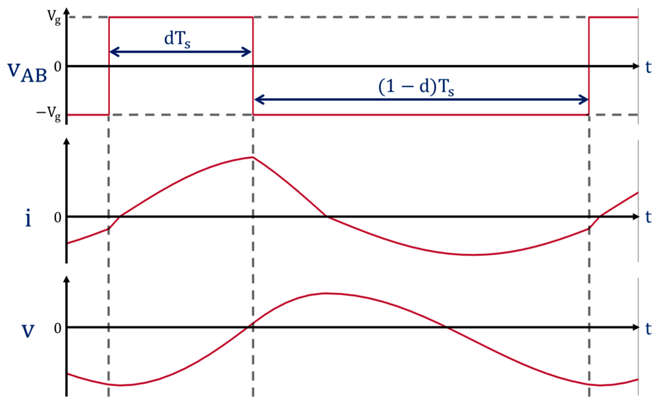
The nonlinear state equations based on the equivalent circuit are derived under the assumption that the resonant tank operates in CCM. The inductor current and capacitor voltage waveforms are depicted in Figure 2, and the governing equations are given by:
v A B = i r s + v + L d i d t + s g n i · n v o
i = C d v d t
1 + r c R L C f d v C f d t + v C f R L = i · n + i o .
The output voltage v o and the average input current i g are expressed as:
v o = r c i · n + i o + r c r c v C f
i g = 1 T s 0 T s i v A B t v g d t
r c = r c · R L r c + R L
where r c is the load resistance and the ESR of the filter capacitor.

2.2. Harmonic Approximation

For harmonic approximation, the resonant inductor current i t and resonant capacitor voltage v t are assumed as follows:
i t = i s t sin ω s t + i c t cos ω s t
v t = V c o + v s t sin ω s t + v c t cos ω s t .
Here, V c o denotes the DC voltage component of the resonant capacitor voltage. Also, i s t , i c t , v s t , and v c t vary slowly over time. Thus, their derivatives are given by:
d i d t = d i s d t ω s i c sin ω s t + d i c d t + ω s i s cos ω s t
d v d t = d v s d t ω s v c sin ω s t + d v c d t + ω s v s cos ω s t .

2.3. Extended Describing Function

Using the EDF method, the nonlinear terms are approximated by DC, sine and cosine components. Here, the filter capacitor voltage v C f closely approximates the output voltage v o due to the negligible filter ESR r c . Therefore, v o is approximated by v C f , allowing the term s g n ( i ) · v o in Equation (4b) to be simplified.
v A B f 1 v g , d + f 2 v g , d sin ω s t + f 3 v g , d cos ω s t
s g n i · v o f 4 i s ,   i c , v C f sin ω s t + f 5 i s , i c , v C f cos ω s t
i f 6 i s , i c
i g f 7 d , i s .
Each f n term is determined by the EDF method based on the operating point and can be derived using Fourier series expansion. As shown in Figure 3, the waveforms of the principal state variables are overwhelmingly governed by their fundamental harmonic. Consequently, the EDF derivation employs only the fundamental component of the Fourier series, which is justified by the fact that SRCs typically operate very close to their resonant frequency.
f 1 = v g 2 d 1
f 2 = 2 v g π 1 cos 2 π d
f 3 = 2 v g π sin 2 π d
f 4 = 4 π i s i p v C f
f 5 = 4 π i c i p v C f
f 6 = 2 π i P
f 7 = 1 π i s 1 cos 2 π d + i c sin 2 π d
where
i P = i s 2 + i c 2 .
In APWM, the Fourier series expansion of v A B includes not only sine components but also DC and cosine components. The DC component, however, is blocked by the series capacitor, resulting in zero current contribution from the DC term.

2.4. Harmonic Balance

To approximate the nonlinear equations, the coefficients obtained through the EDF method and the harmonic approximations are substituted into the system equations, resulting in the following expressions:
i s r s + v c + L d i s d t ω s i c + 4 π i s i p n · v C f = V e s
i c r s + v s + L d i c d t + ω s i s + 4 π i c i p n · v C f = V e c
C d v s d t ω s v c = i s
C d v c d t + ω s v s = i c
1 + r c R L C f d v C f d t + v C f R L = 2 n π i P + i o
V e s = 2 v g π 1 cos 2 π d
V e c = 2 v g π sin 2 π d
V c o = v g 2 d 1 .
The output voltage v o and input current i g can be expressed as:
v o = r c 2 n π i P + i o + r c r c v C f
i g = 1 π i s 1 cos 2 π d + i c sin 2 π d .

2.5. Steady-State Solution

In steady state, i s , i c , v s , v c ,   v C f become time-invariant and are denoted by the constant I s , I c , V s , V c , V C f . Likewise, the operating-point v g , d , ω s is represented by V g , D , Ω s . Setting all time derivatives and the disturbance current i o to zero yields the steady-state solution given by:
V s = V e s α + V e c β α 2 + β 2
V c = V e c α V e s β α 2 + β 2
I s = Ω s V c
I c = Ω s V s
V C f = π 4 n I P R e
where
α = 1 Ω s 2 L C
β = Ω s C R e + r s
R e = 8 n 2 π 2 R L
I p = I s 2 + I c 2
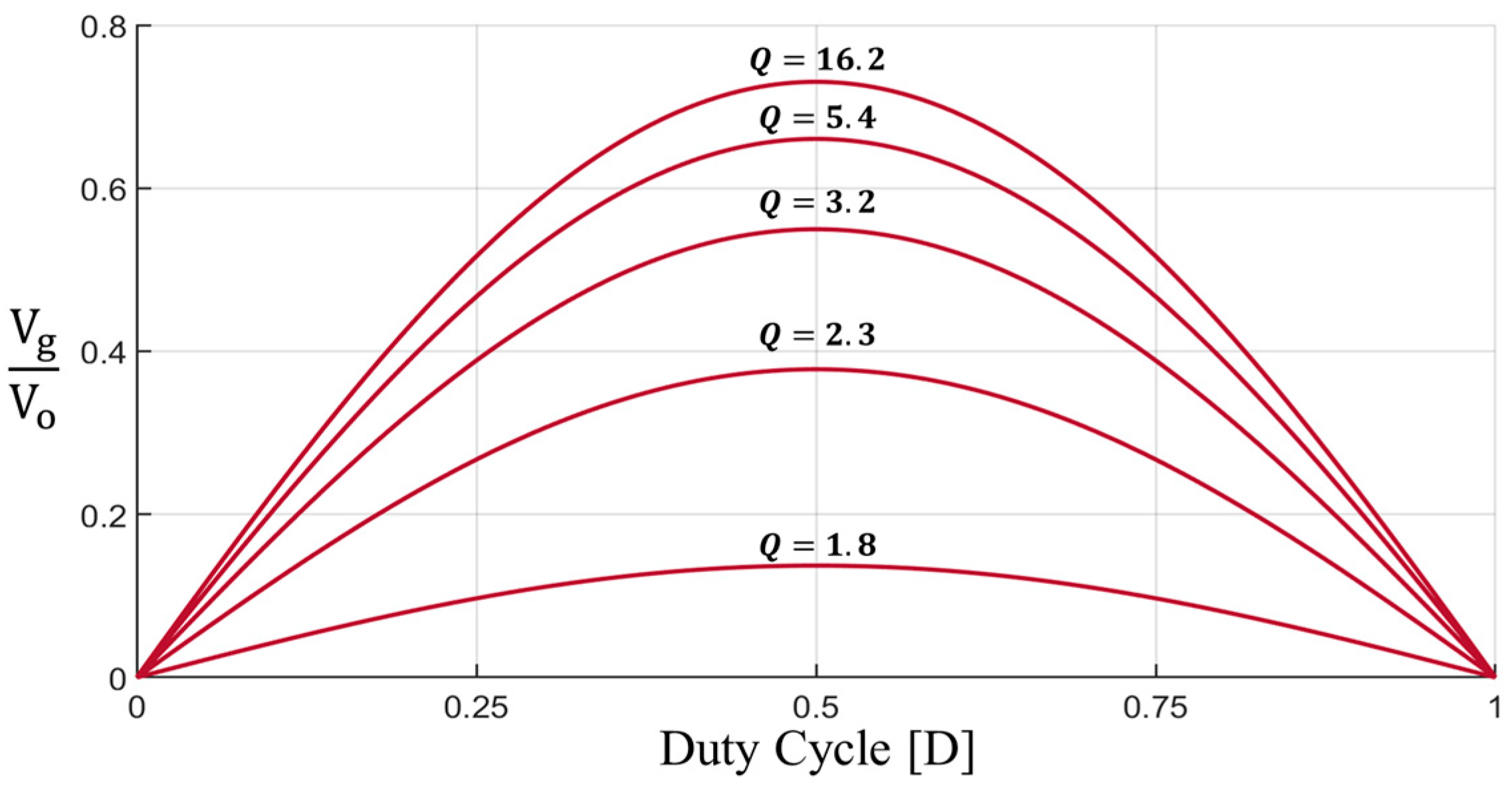
Figure 4 shows the voltage conversion ratio under APWM control with a fixed switching frequency. The APWM voltage conversion ratio is symmetric about a duty cycle of 0.5, increasing from its minimum at D = 0 to its maximum at D = 0.5 , and then decreasing symmetrically from D = 0.5 back to its minimum at D = 1 . In this paper, the analysis is conducted over the duty cycle range 0 D 0.5 .
For further details on the voltage conversion ratio, the reader is referred to Reference [7].

2.6. Perturbation and Linearization

For perturbation and linearization, small-signal deviations are assumed around the steady-state operating point as follows:
v g = V g + v ^ g ,     d = D + d ^ ,     ω s = Ω s + ω ^ s ,     i o = I o + i ^ o .
The small-signal model is defined as:
d x ^ d t = A x ^ + B u ^
y = C x ^ + E u ^ .
Here, the state vector x , input vector u , and output vector y are given as:
x ^ = i ^ s i ^ c v ^ s v ^ c v ^ C f T
u ^ = v ^ g d ^ ω ^ s i ^ o T
y ^ = v ^ o i ^ g T .
After linearization, the state-space model matrices A, B, C, and E are derived, where all parameters such as R s , R c , Z s , Z c , k s , k c , k v s , k v c , E d s , E d c , and I d are expressed in terms of steady-state variables.
A = R s L Z s L 1 L 0 2 k s L Z c L R c L 0 1 L 2 k c L 1 C 0 0 Ω s 0 0 1 C Ω s 0 0 k s r c C f r c k c r c C f r c 0 0 r c C f r c
B = k v s L E d s L I c 0 k v c L E d c L I s 0 0 0 V c 0 0 0 V s 0 0 0 0 r c C f r c
C = r c k s r c k c 0 0 r c r c 1 π 1 cos 2 π D 1 π sin 2 π D 0 0 0
E = 0 0 0 r c 0 I d 0 0
R s = r s + 4 n π I c 2 I P 3 V C f
R c = r s + 4 n π I s 2 I P 3 V C f
Z s = Ω s L + 4 n π I s I c I P 3 V C f
Z c = Ω s L 4 n π I s I c I p 3 V C f
k s = 2 n π I s I P
k c = 2 n π I c I P
k v s = 2 π 1 cos 2 π D
k v c = 2 π sin 2 π D
E d s = 4 V g sin 2 π D
E d c = 4 V g cos 2 π D
I d = 2 I s sin 2 π D + I c cos 2 π D

3. Simulation and Experimental Results

3.1. Simulation Results

Based on Equations (6g)–(6j), the transfer functions derived from the analytical model were implemented and simulated in MATLAB(R2024a) to validate the proposed small-signal model. Thereafter, PLECS(4.7.5) simulations were carried out by injecting small-signal perturbations into the circuit and measuring the frequency response at the nominal operating point to corroborate the MATLAB results. The circuit parameters used for all simulations are summarized in Table 1.
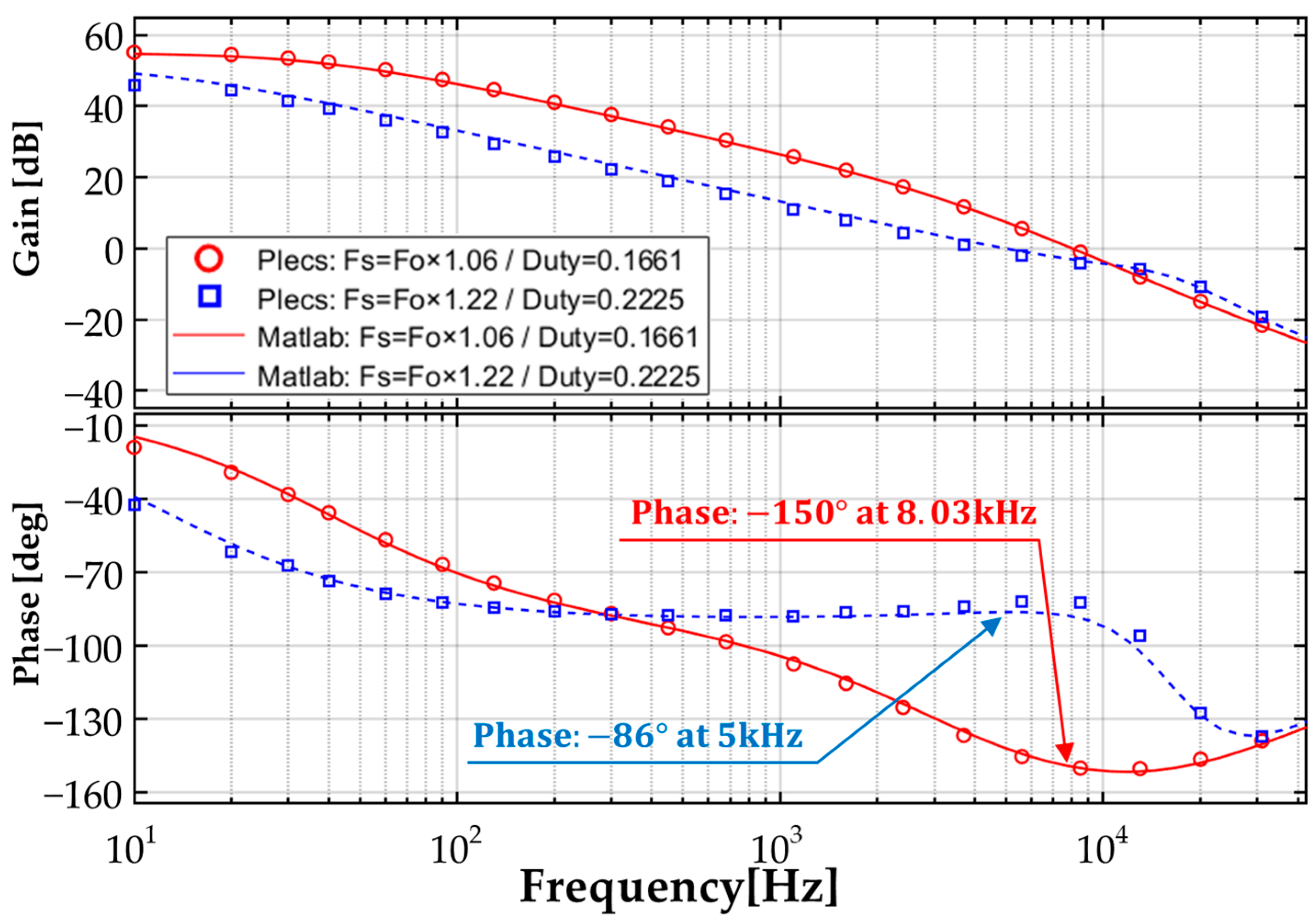
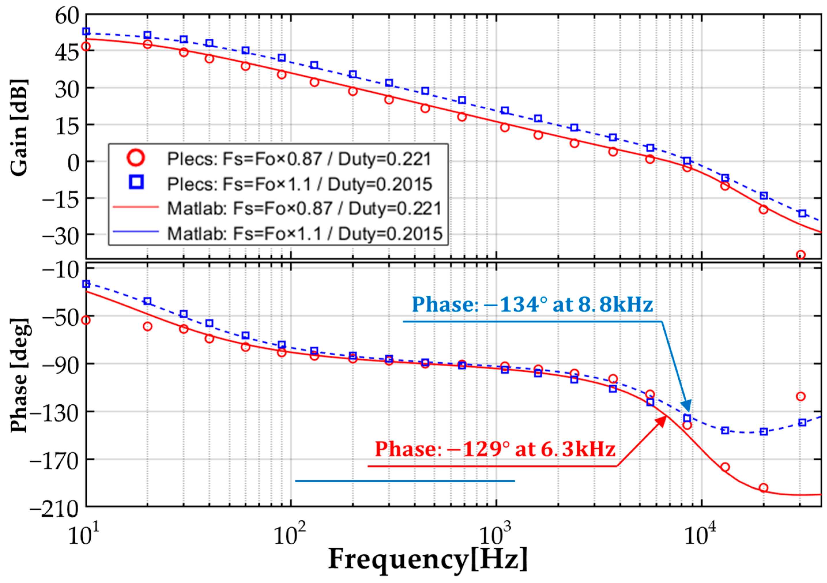
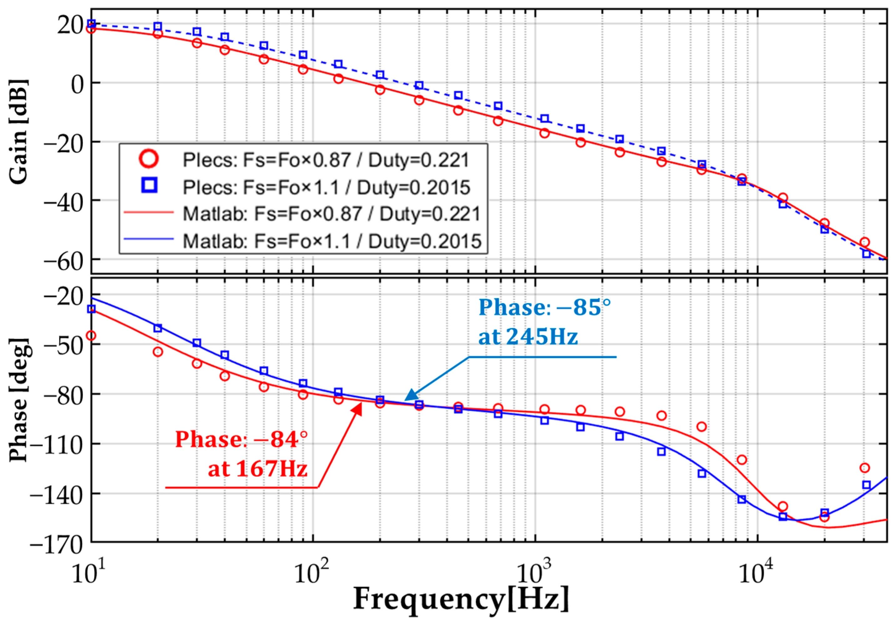
Figure 5 and Figure 6 depict the simulation results used to validate the Control(Duty)-to-Output transfer function v ^ o d ^ . This transfer function characterizes the dynamic relationship between small perturbations in the duty cycle d ^ and the resulting output voltage response v ^ o .
Simulation accuracy was evaluated at multiple steady-state operating points to validate the proposed small-signal model. in Figure 5, for a load resistance of R L = 600   Ω , two switching to resonant frequency ratios F s F o of 1.06 and 1.22 corresponding to 74 kHz and 85 kHz, respectively, were selected. The duty cycle D was set to 0.1661 at 74 kHz and 0.2225 at 85 kHz to maintain V o = 100   V . Figure 6 shows results for R L = 400   Ω , with F s F o = 0.87 (61 kHz) and 1.10 (77 kHz), where the duty cycle D was adjusted to 0.221 and 0.2015, respectively, to achieve the same output voltage.
In each Bode plot, the phase angle at the unity-gain crossover frequency is annotated. A direct comparison of MATLAB and PLECS derived responses across all four cases reveals nearly identical gain crossover points and phase profiles, confirming the high fidelity of the small-signal model.
The simulation results presented in Figure 7 and Figure 8 were used to validate the Line-to-Output transfer function v ^ o v ^ g . This transfer function characterizes the output voltage response v ^ o to small-signal perturbations in the input voltage v ^ g and is employed to analyze the impact of input voltage disturbances on the output voltage.
The operating points for the Line-to-Output simulations were chosen as in Figure 5 and Figure 6. Figure 7 and Figure 8 present the MATLAB and PLECS derived response of the Line-to-Output transfer function, confirming excellent agreement in comparison. Accordingly, the accuracy of the transfer function was validated in simulation. Each Bode plot annotates the phase angle at the unity-gain crossover frequency.
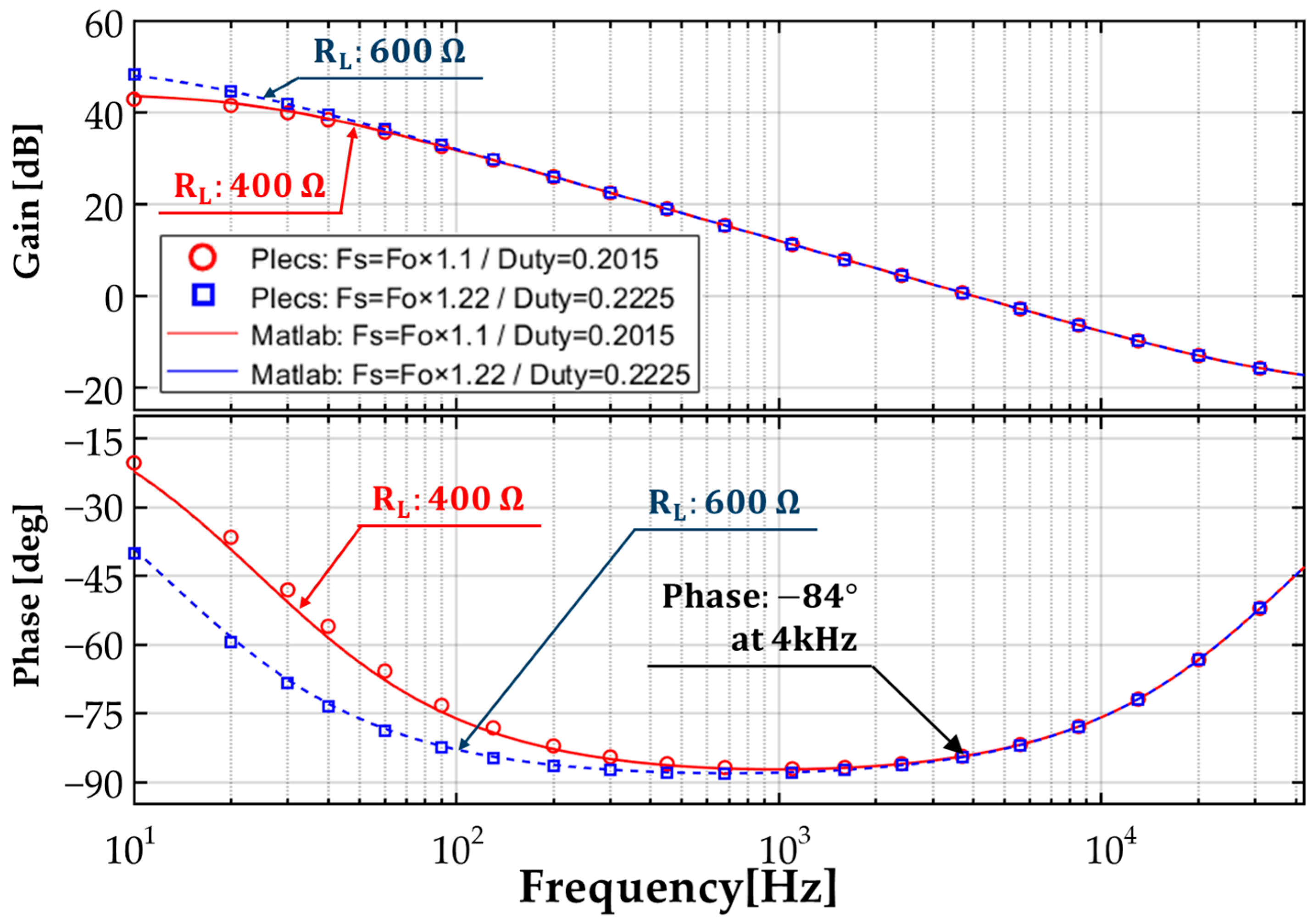
Figure 9 presents the simulation results used to validate the Output Impedance transfer function v ^ o i ^ o . This function characterizes the output voltage response v ^ o due to load disturbances i ^ o and provides key information for assessing system stability.
The operating points were chosen as follows. For R L = 400   Ω , the switching frequency was set to F s = 1.10 · F o (77 kHz) and the duty cycle to D = 0.2015 to maintain V o = 100   V . For R L = 600   Ω , F s = 1.22 · F o (85 kHz) and D = 0.2225 were used for the same nominal output voltage.
A direct comparison of MATLAB and PLECS derived Bode plots in Figure 9 demonstrates excellent agreement, thereby validating the accuracy of the proposed small-signal model’s Output Impedance transfer function.

3.2. Experimental Results

To further validate the transfer functions confirmed in the simulation results sections, experimental measurements were carried out. The SRC was configured with the parameters listed in Table 1. Gate signals were generated using a DSP control board based on the TMS320F28335. Power switching was implemented with GS66508T GaN transistors (Infineon Technologies, Neubiberg, Germany, 650 V, 30 A), and rectification employed MURS160-13-F diodes (Diodes Incorporated, Texas Plano, TX, USA, 600 V, 1 A). The resonant inductor comprised five turns wound on a powder-magnetic core (ChangSung, Incheon, Republic of Korea), and two film capacitors were used in both the resonant tank and the output filter. Frequency-response measurements were performed using a PSM1700 Frequency Response Analyzer (Newtons4th Ltd., Leicester, UK). Parasitic and loss elements such as the GS66508T GaN transistor’ R D S , winding resistances of the inductor and transformer, and capacitor dissipation factor were neglected.
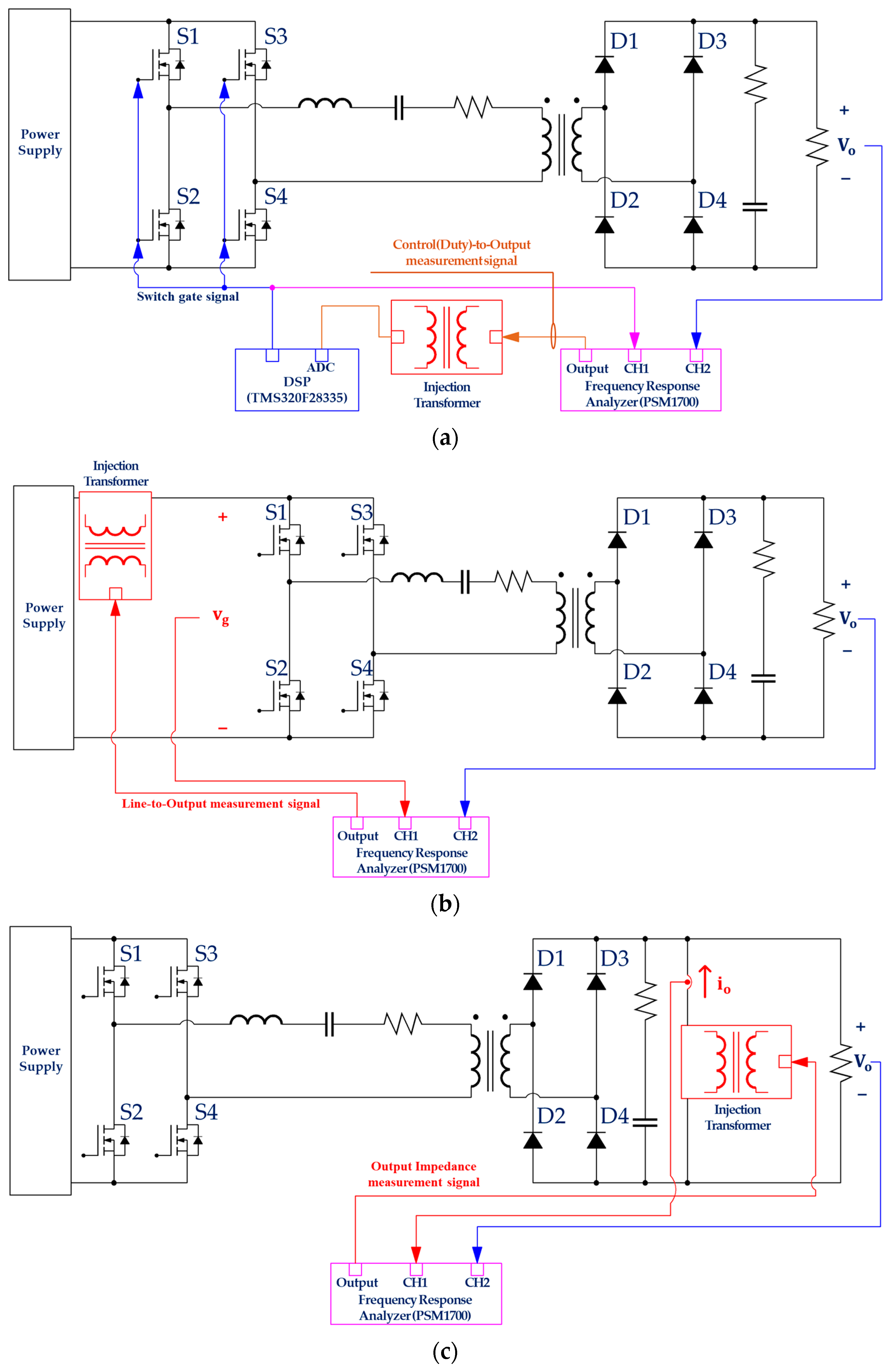
Figure 10 illustrates the hardware configuration of the PSM1700 Frequency Response Analyzer used for measuring each transfer function. In the Control(Duty)-to-Output experiment, the analyzer’s excitation output was routed into the DSP board’s ADC, and the DSP superimposed this signal onto the duty-cycle reference before generating the corresponding gate-drive commands for the GaN transistors. The resulting output voltage was sensed by the PSM1700 Frequency Response Analyzer and measured on CH2, while the gate-drive waveform was measured on CH1 to compensate for phase delay. For the Line-to-Output experiment, the excitation output was injected in series with the SRC’s input power line via an injection transformer to impose small disturbances on v ^ g , and the perturbed output voltage was connected in parallel with the load to introduce perturbations in the load current i ^ o , and the resulting variation in v ^ o was similarly captured on CH2.
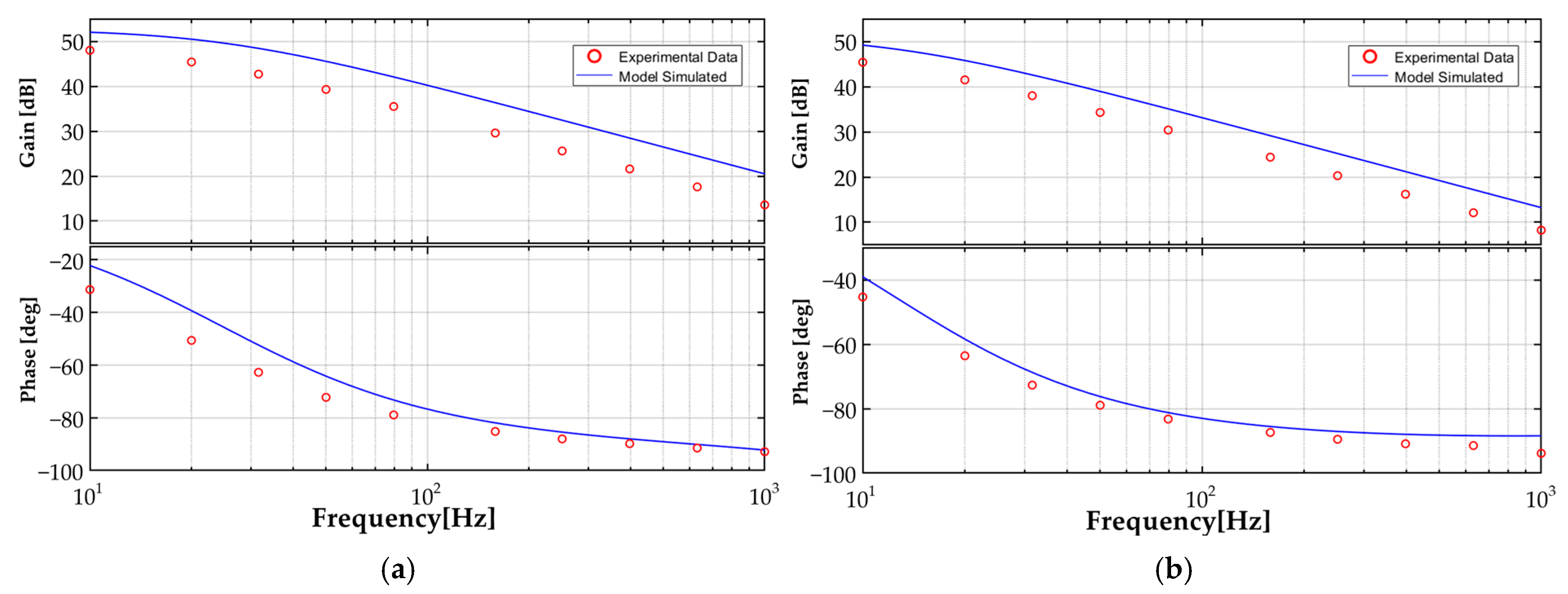
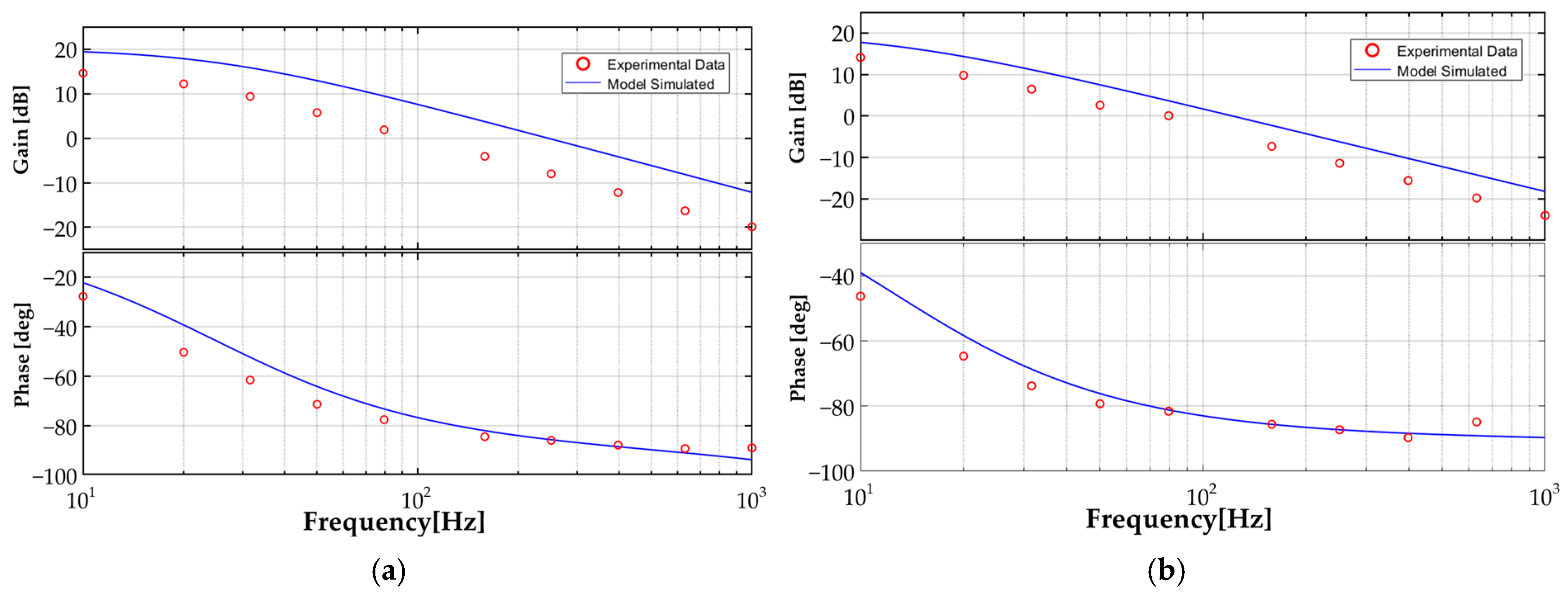
Despite gain and phase discrepancies introduced by unmodeled losses and parasitic elements, the experimental data are sufficient to validate the proposed small-signal model. Measurements for each transfer function were conducted at an output voltage of V o = 100   V under two operating conditions: R L = 400   Ω , F s = 76.8   k H z , D = 0.2015 ; and R L = 600   Ω , F s = 85   k H z , D = 0.2225 . Figure 11 presents the Control(Duty)-to-Output measurements and MATLAB simulations, wherein the experimental frequency-response curves closely follow their simulated counterparts, thereby confirming the model’s accuracy. Figure 12 shows the Line-to-Output measurements and simulations at the same operating points, again demonstrating that the experimental curves track the simulations and validate accuracy. Figure 13 depicts the Output Impedance measurements and simulations under identical conditions, likewise revealing close agreement between experimental and simulated curves and validating the transfer function accuracy. Thus, all three transfer functions derived in the simulation section have been experimentally validated.

4. Conclusions

This paper presents an EDF-based small-signal model for an APWM SRC operating in CCM. The EDF method was applied to approximate the nonlinear state equations by representing both DC, cosine term harmonic components, and the resulting approximated equations were perturbed and linearized to derive the small-signal model. The model’s accuracy is validated by comparing the Control(Duty)-to-Output, Line-to-Output, and Output Impedance transfer functions against MATLAB and PLECS simulations and further confirmed by experimental measurements. The proposed small-signal model thus provides precise transfer functions. These transfer functions can be used to extract gain and phase characteristics and to evaluate stability margins for optimized feedback controller design in APWM-controlled SRCs.

Author Contributions

Conceptualization, G.-M.P.; methodology, G.-M.P.; software, G.-M.P.; validation, G.-M.P.; investigation, G.-M.P.; data curation, G.-M.P.; writing—original draft preparation, G.-M.P.; writing—review and editing, K.-J.L.; supervision, K.-J.L.; project administration, K.-J.L. All authors have read and agreed to the published version of the manuscript.

Funding

This work was supported by the Korea Institute of Energy Technology Evaluation and Planning (KETEP) grant funded by the Ministry of Trade, Industry and Energy (MOTIE) (RS-2024-00394769). This work was supported by Human Resources Development of the Korea Institute of Energy Technology Evaluation and Planning (KETEP) grant funded by the Korea government. (No. 20224000000070).

Data Availability Statement

The original contributions presented in this study are included in the article. Further inquiries can be directed to the corresponding author.

Conflicts of Interest

The authors declare no conflict of interest.

References

  1. Kim, J.-W.; Barbosa, P. PWM-Controlled Series Resonant Converter for Universal Electric Vehicle Charger. IEEE Trans. Power Electron. 2021, 12, 13578–13588. [Google Scholar] [CrossRef]
  2. Dao, N.D.; Lee, D.-C.; Phan, Q.D. High-Efficiency SiC-Based Isolated Three-Port DC/DC Converters for Hybrid Charging Stations. IEEE Trans. Power Electron. 2020, 10, 10455–10465. [Google Scholar] [CrossRef]
  3. Kwon, Y.D.; Freijedo, F.D.; Wijekoon, T.; Liserre, M. Series Resonant Converter-Based Full-Bridge DC–DC Partial Power Converter for Solar PV. IEEE J. Emerg. Sel. Top. Power Electron. 2024, 2, 1719–1729. [Google Scholar] [CrossRef]
  4. Shen, Y.; Wang, H.; Al-Durra, A.; Qin, Z.; Blaabjerg, F. A Structure-Reconfigurable Series Resonant DC–DC Converter with Wide-Input and Configurable-Output Voltages. IEEE Trans. Ind. Electron. 2019, 2, 1752–1764. [Google Scholar] [CrossRef]
  5. Lee, K.-J. Steady-State Analysis of Asymmetrical Pulse-Width-Modulated Series Resonant Converter for Light Load Condition. Electronics 2025, 14, 63. [Google Scholar] [CrossRef]
  6. Jain, P.K.; St-Martin, A.; Edwards, G. Asymmetrical pulse-width-modulated resonant DC/DC converter topologies. IEEE Trans. Power Electron. 1996, 3, 413–422. [Google Scholar] [CrossRef]
  7. Ryu, S.-H.; Kim, D.-H.; Kim, M.-J.; Kim, J.-S.; Lee, B.-K. Adjustable Frequency–Duty-Cycle Hybrid Control Strategy for Full-Bridge Series Resonant Converters in Electric Vehicle Chargers. IEEE Trans. Ind. Electron. 2014, 10, 5354–5362. [Google Scholar]
  8. Park, H.-P.; Kim, M.; Jung, J.-H. Bidirectional Current-Fed CLLC Resonant Converter Employing Asymmetric PWM. IEEE Trans. Energy Conver. 2021, 4, 3167–3177. [Google Scholar] [CrossRef]
  9. Chen, G.; Chen, Z.; Chen, Y.; Feng, C.; Zhu, X. Asymmetric Phase-Shift Modulation Strategy of DAB Converters for Improved Light-Load Efficiency. IEEE Trans. Power Electron. 2022, 8, 9104–9113. [Google Scholar] [CrossRef]
  10. Mahdavifard, M.; Mazloum, N.; Zahin, F.; KhakparvarYazdi, A.; Abasian, A.; Khajehoddin, S.A. An Asymmetrical DAB Converter Modulation and Control Systems to Extend the ZVS Range and Improve Efficiency. IEEE Trans. Power Electron. 2022, 10, 12774–12792. [Google Scholar] [CrossRef]
  11. Pont, N.C.D.; Bandeira, D.G.; Lazzarin, T.B.; Barbi, I. A ZVS APWM Half-Bridge Parallel Resonant DC–DC Converter with Capacitive Output. IEEE Trans. Power Electron. 2019, 7, 5231–5241. [Google Scholar] [CrossRef]
  12. Awasthi, A.; Bagawade, S.; Kumar, A.; Jain, P. Time-Domain Analysis of APWM-Frequency Modulated Low-Q LLC Resonant Converter for Wide Input and Load Range Applications. In Proceedings of the 2019 IEEE Energy Conversion Congress and Exposition (ECCE), Baltimore, MD, USA, 29 September–3 October 2019; pp. 1334–1340. [Google Scholar]
  13. Guo, Z.; Zhu, Y.; Sha, D. Zero-Voltage-Switching Asymmetrical PWM Full-Bridge DC–DC Converter with Reduced Circulating Current. IEEE Trans. Ind. Electron. 2021, 5, 3840–3853. [Google Scholar] [CrossRef]
  14. Yang, E.X.; Lee, F.C.; Jovanovic, M.M. Small-signal modeling of series and parallel resonant converters. In Proceedings of the APEC ‘92 Seventh Annual Applied Power Electronics Conference and Exposition, Boston, MA, USA, 23–27 February 1992; pp. 785–792. [Google Scholar]
  15. Chang, C.-H.; Chang, E.-C.; Cheng, C.-A.; Cheng, H.-L.; Lin, S.-C. Small Signal Modeling of LLC Resonant Converters Based on Extended Describing Function. In Proceedings of the 2012 International Symposium on Computer, Consumer and Control, Taichung, Taiwan, 4–6 June 2012; pp. 365–368. [Google Scholar]
  16. Tian, S.; Lee, F.C.; Li, Q. Equivalent Circuit Modeling of LLC Resonant Converter. IEEE Trans. Power Electron. 2020, 8, 8833–8845. [Google Scholar] [CrossRef]
  17. Yuan, J.; Wang, N.; Wang, X.; Wang, F.; Liu, M. A Small-Signal Modeling Method for Bidirectional CLLC Resonant Converter. In Proceedings of the IECON 2023—49th Annual Conference of the IEEE Industrial Electronics Society, Singapore, 16–19 October 2023; pp. 1–6. [Google Scholar]
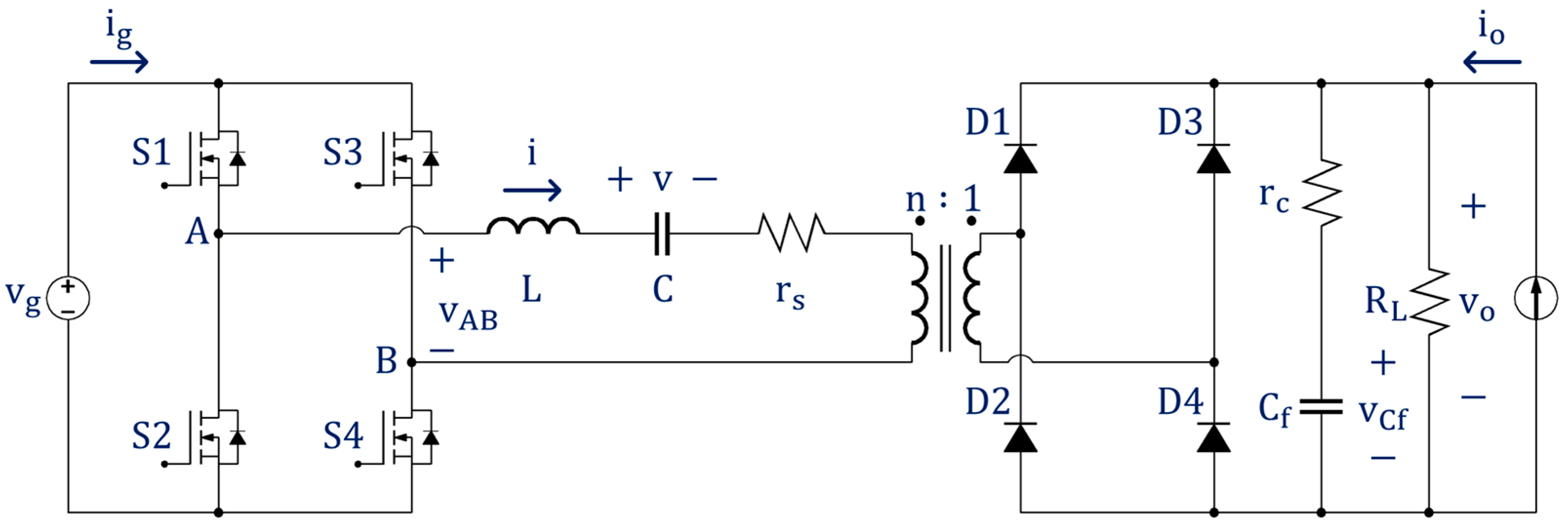
Figure 1. Equivalent circuit of full-bridge series resonant converter.
Electronics 14 03394 g001
Figure 2. Waveforms of inductor current, capacitor voltage.
Electronics 14 03394 g002
Figure 3. Frequency spectrum of inductor current, capacitor voltage, switching voltage.
Electronics 14 03394 g003
Figure 4. Voltage conversion ratio for asymmetric pulse width modulation.
Electronics 14 03394 g004
Figure 5. Verification of Control(Duty)-to-Output transfer function ( R L = 600   Ω , V o = 100   V ).
Electronics 14 03394 g005
Figure 6. Verification of Control(Duty)-to-Output transfer function ( R L = 400   Ω , V o = 100   V ).
Electronics 14 03394 g006
Figure 7. Verification of Line-to-Output transfer function ( R L = 600   Ω , V o = 100   V ).
Electronics 14 03394 g007
Figure 8. Verification of Line-to-Output transfer function ( R L = 400   Ω , V o = 100   V ).
Electronics 14 03394 g008
Figure 9. Verification of Output Impedance transfer function ( V o = 100   V ).
Electronics 14 03394 g009
Figure 10. Experimental hardware configuration for measuring ((a) Control(Duty)-to-Output, (b) Line-to-Output, (c) Output Impedance).
Electronics 14 03394 g010
Figure 11. Experimental Verification of Control(Duty)-to-Output transfer function for V o = 100   V ((a) R L = 400   Ω , (b) R L = 600   Ω ).
Electronics 14 03394 g011
Figure 12. Experimental Verification of Line-to-Output transfer function for V o = 100   V ((a) R L = 400   Ω , (b) R L = 600   Ω ).
Electronics 14 03394 g012
Figure 13. Experimental Verification of Output Impedance transfer function for V o = 100   V ((a) R L = 400   Ω , (b) R L = 600   Ω ).
Electronics 14 03394 g013
Table 1. System parameters.
V g 10   V n 1 / 24
L 5.2   μ H C 1   μ F
r s 0.1   Ω r c 0.1   Ω
C f 40   μ F F o 69.8   k H z
Disclaimer/Publisher’s Note: The statements, opinions and data contained in all publications are solely those of the individual author(s) and contributor(s) and not of MDPI and/or the editor(s). MDPI and/or the editor(s) disclaim responsibility for any injury to people or property resulting from any ideas, methods, instructions or products referred to in the content.