
Design and Evaluation of Radiation-Tolerant 2:1 CMOS Multiplexers in 32 nm Technology Node: Transistor-Level Mitigation Strategies and Performance Trade-Offs


Abstract
1. Introduction
2. Background
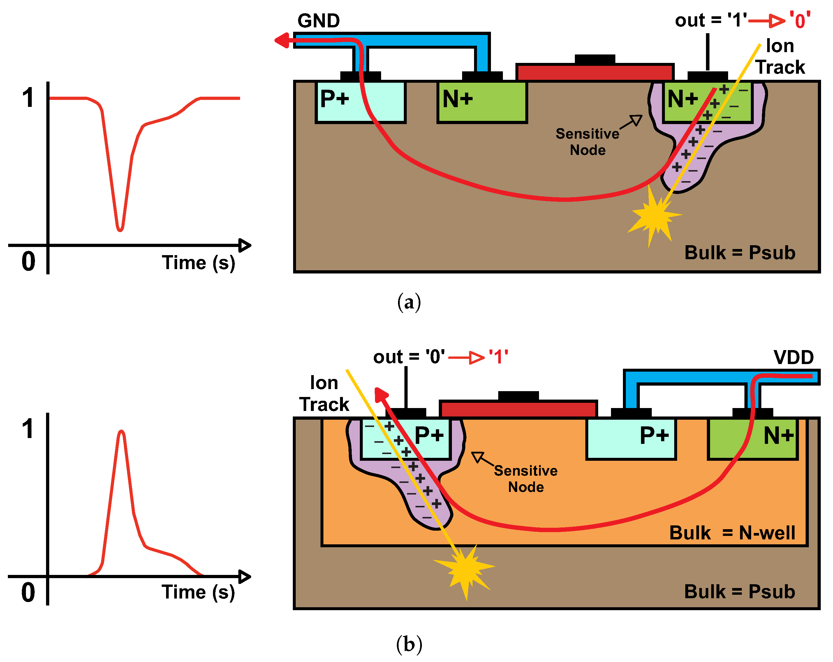
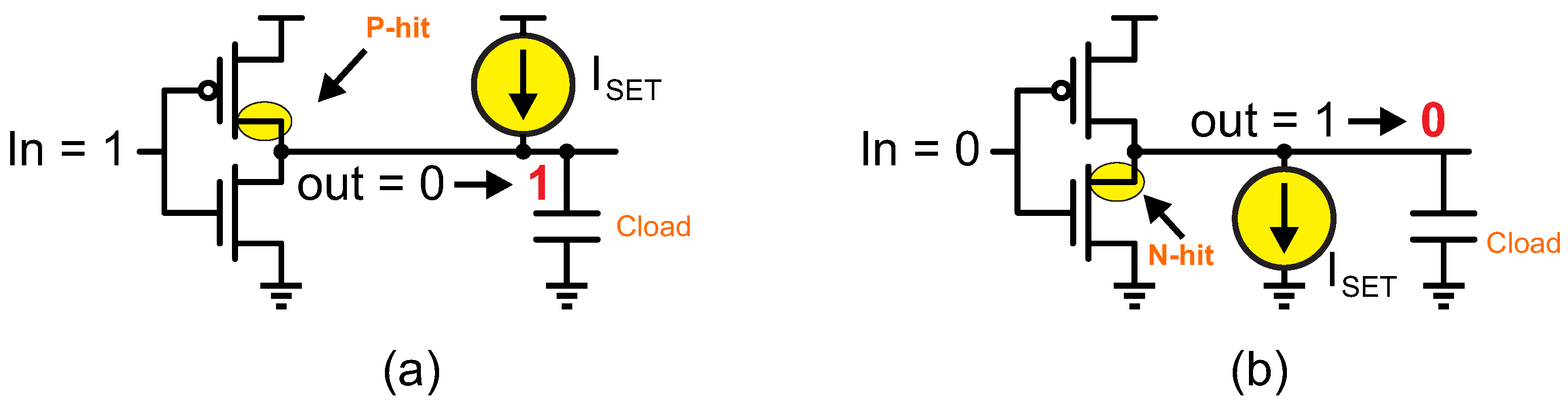
2.1. Single-Event Effects
2.2. Circuit-Level Fault Mitigation Techniques
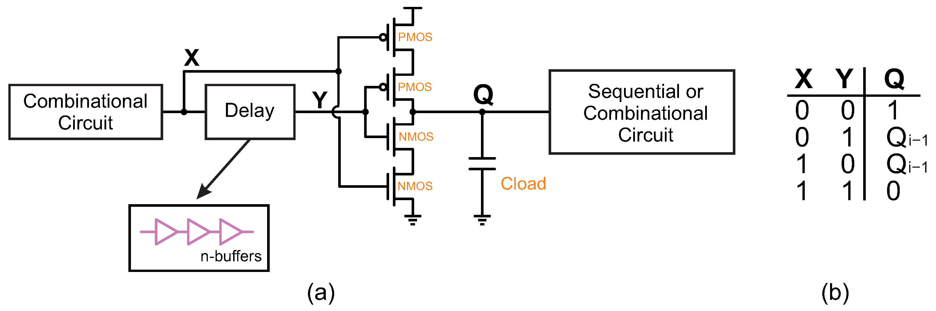
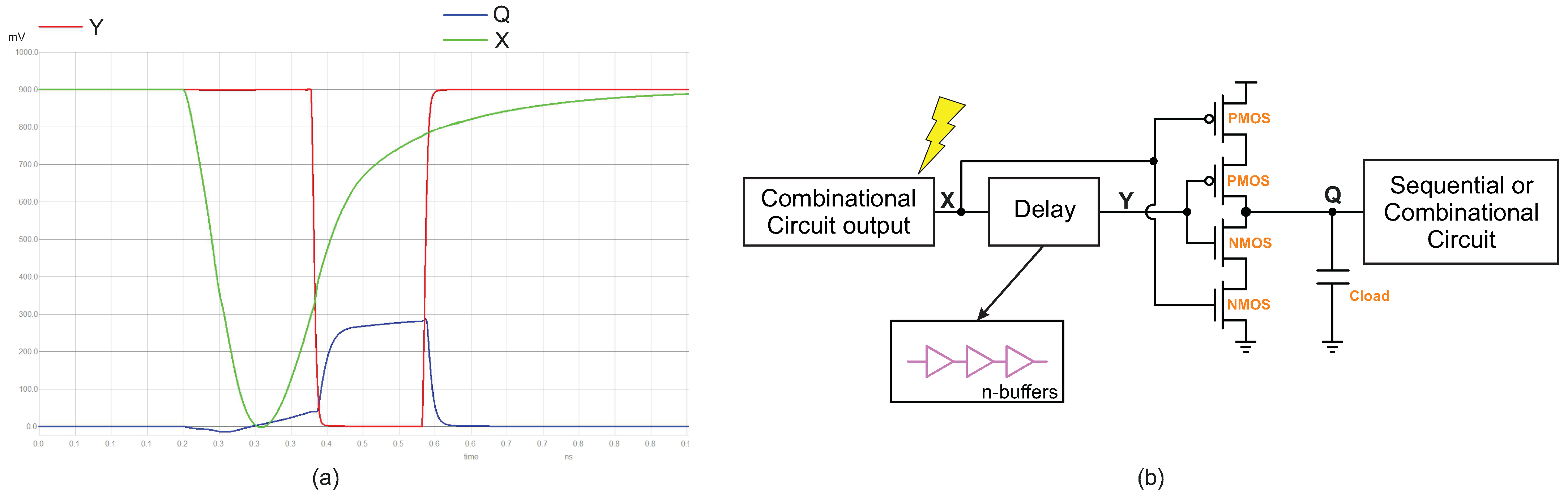
2.2.1. C-Element
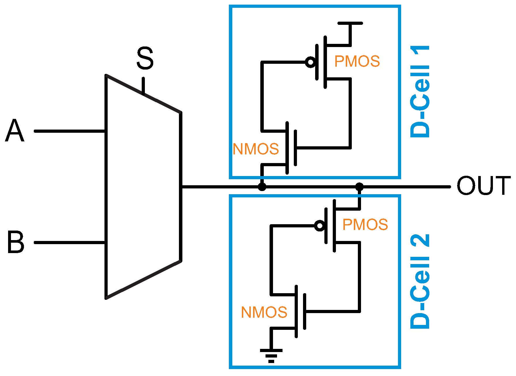
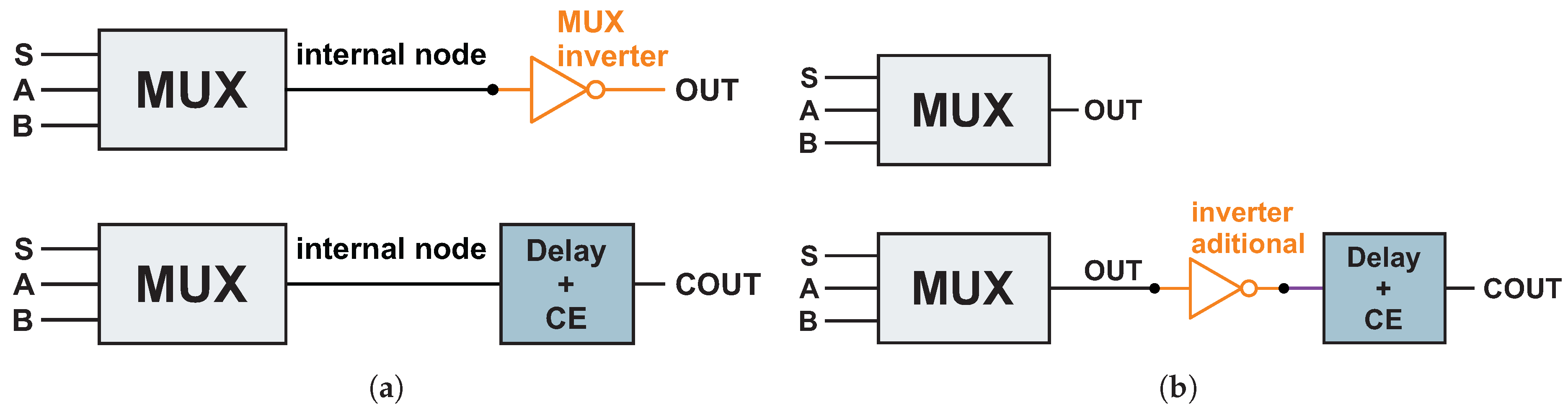
2.2.2. Decoupling Cell
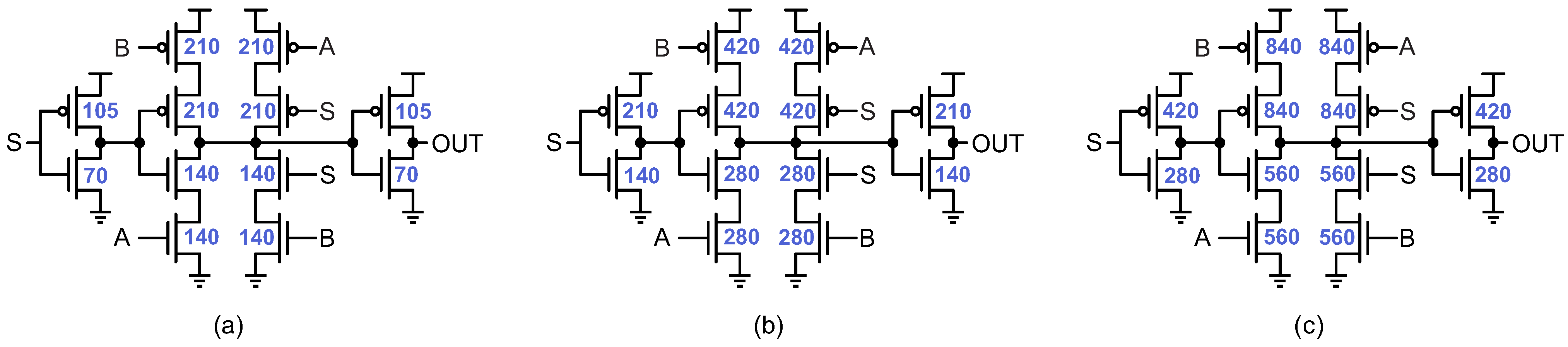
2.2.3. Transistor Sizing
2.3. Related Work
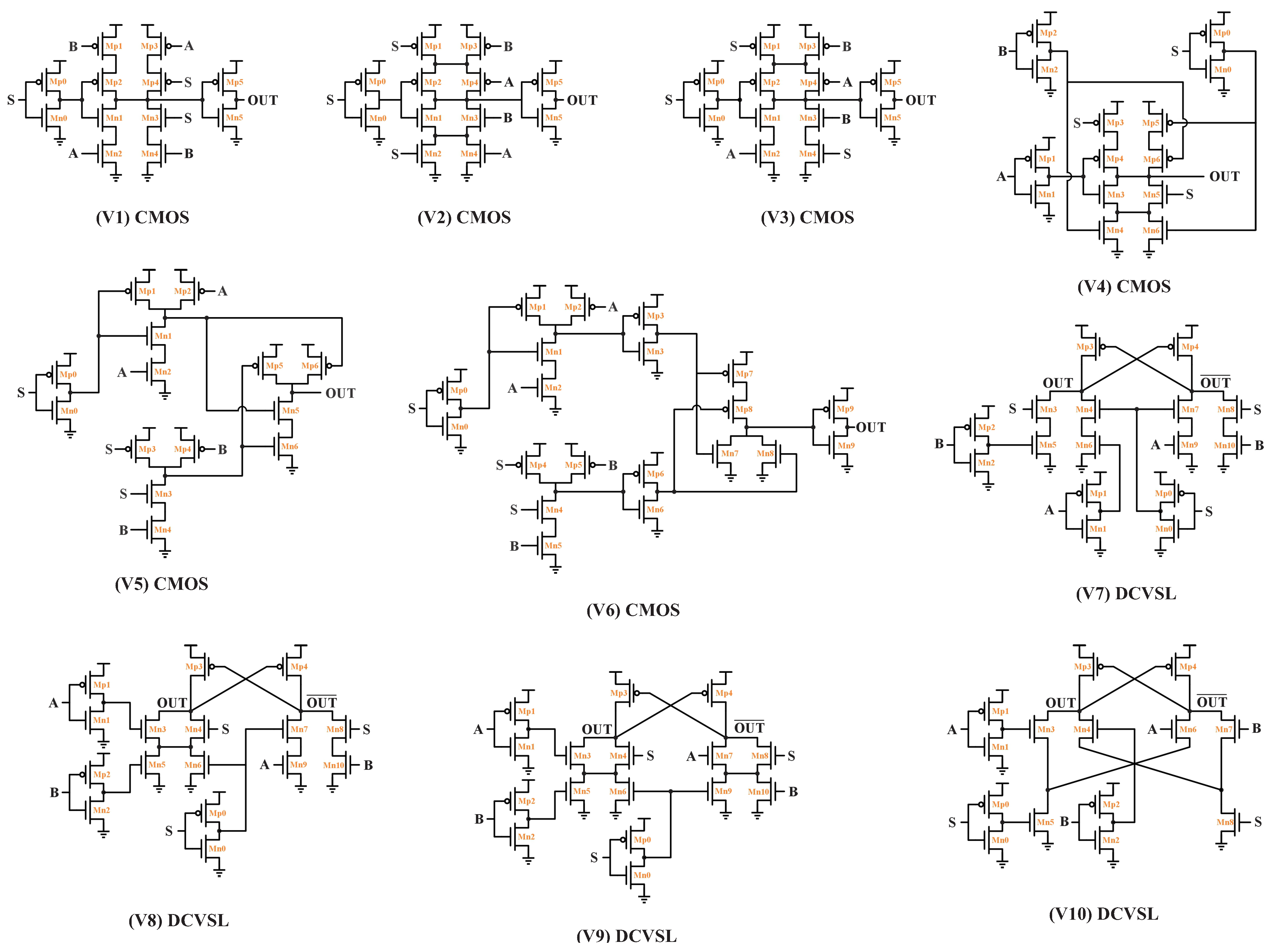
3. Methodology
4. Results
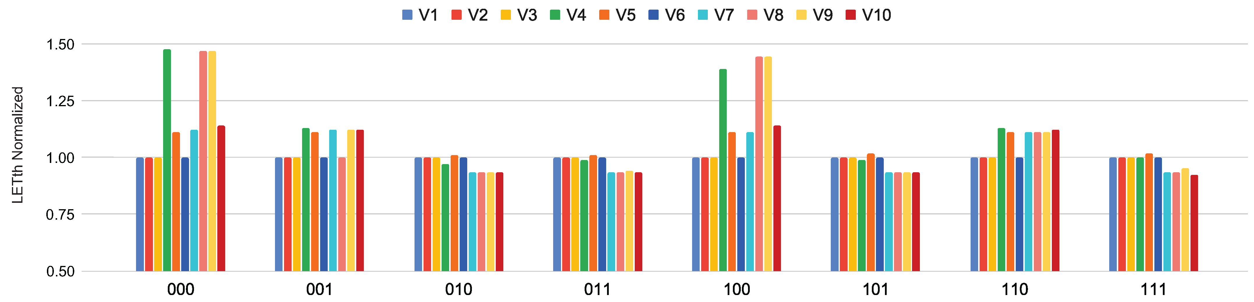
4.1. LET Impact
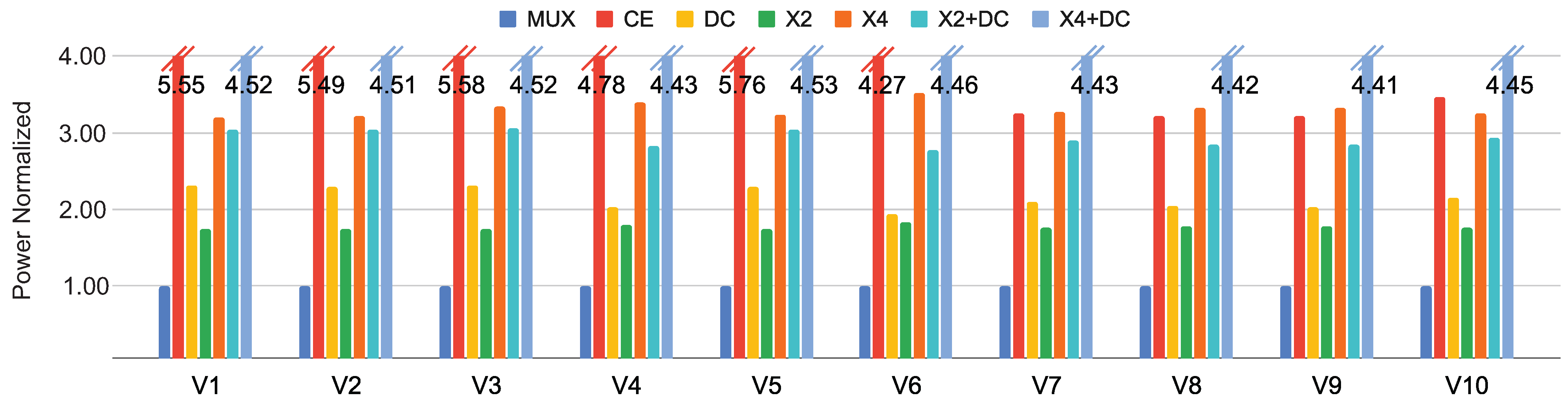
4.2. Power Consumption Impact
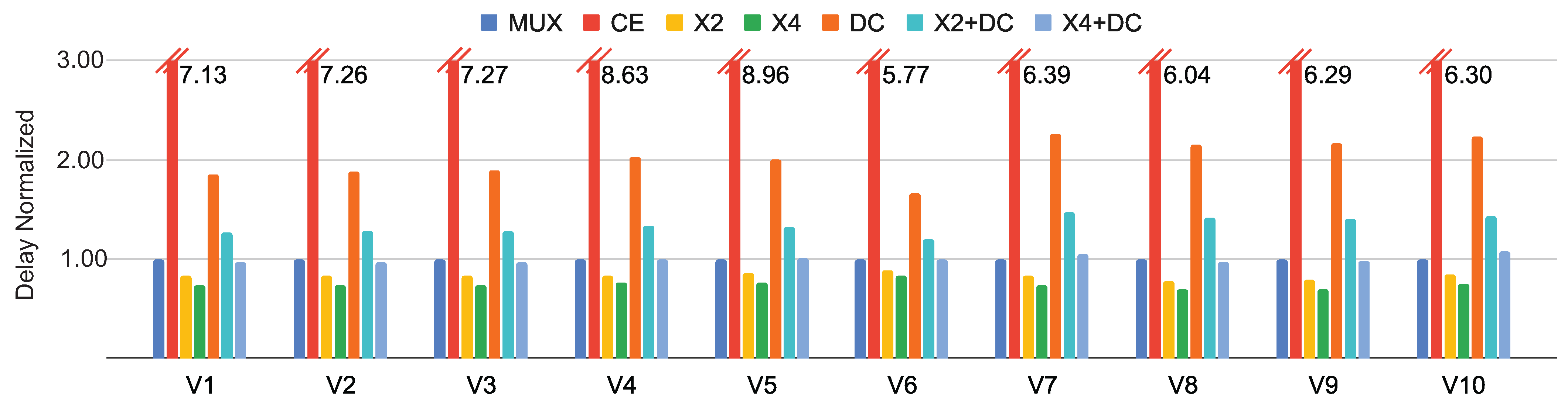
4.3. Delay Impact
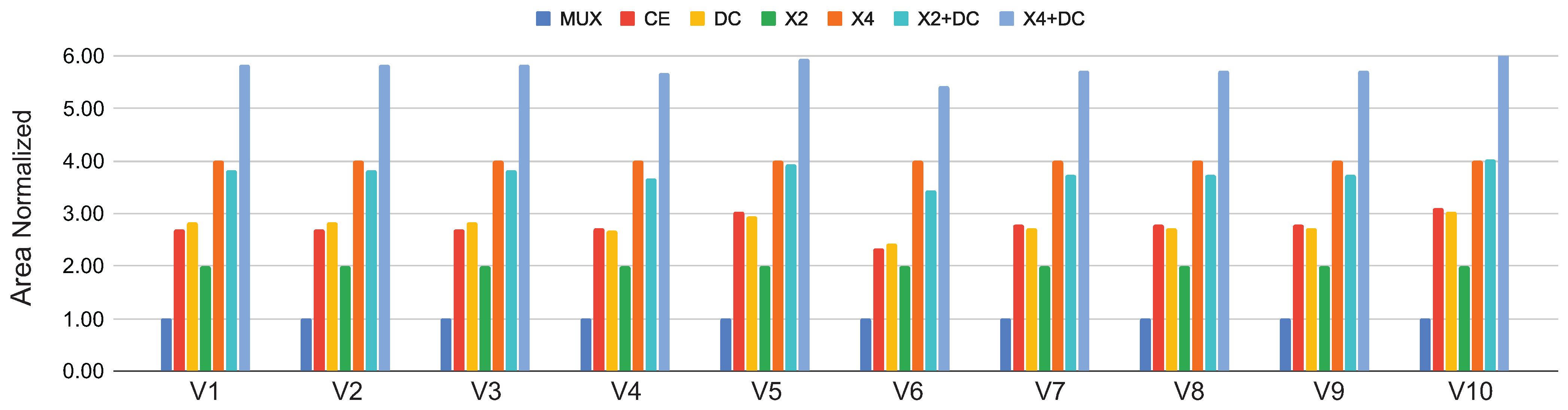
4.4. Area Impact
5. Overall Trade-Off Discussion
6. Conclusions
Author Contributions
Funding
Data Availability Statement
Acknowledgments
Conflicts of Interest
References
- Benedetto, J.; Eaton, P.; Mavis, D.; Gadlage, M.; Turflinger, T. Digital single event transient trends with technology node scaling. IEEE Trans. Nucl. Sci. 2006, 53, 3462–3465. [Google Scholar] [CrossRef]
- Dodd, P.; Shaneyfelt, M.; Schwank, J.; Felix, J. Current and future challenges in radiation effects on CMOS electronics. IEEE Trans. Nucl. Sci. 2010, 57, 1747–1763. [Google Scholar] [CrossRef]
- Hughes, H.; Benedetto, J. Radiation effects and hardening of MOS technology: Devices and circuits. IEEE Trans. Nucl. Sci. 2003, 50, 500–521. [Google Scholar] [CrossRef]
- Messenger, G. Collection of charge on junction nodes from ion tracks. IEEE Trans. Nucl. Sci. 1982, 29, 2024–2031. [Google Scholar] [CrossRef]
- Dodd, P.E.; Massengill, L.W. Basic mechanisms and modeling of single-event upset in digital microelectronics. IEEE Trans. Nucl. Sci. 2003, 50, 583–602. [Google Scholar] [CrossRef]
- Pannu, N.; Prakash, N.R. Modeling and simulation of low power single event upset-resilient SRAM cell. Analog. Integr. Circuits Signal Process. 2025, 122, 19. [Google Scholar] [CrossRef]
- Schwank, J.R.; Rodbell, K.P.; Heidel, D.F.; Pellish, J.A.; Marshall, P.W.; Tang, H.H.; Murray, C.E.; LaBel, K.A.; Gordon, M.S.; Stawiasz, K.G.; et al. 32 and 45 nm Radiation-Hardened-By-Design (RHBD) SOI Latches; Technical Report; Sandia National Lab. (SNL-NM): Albuquerque, NM, USA, 2011. [Google Scholar]
- Oliveira, R.N.M.; da Silva, F.G.R.G.; Reis, R.; Schvittz, R.B.; Meinhardt, C. Improving Soft Error Robustness of Full Adder Circuits with Decoupling Cell and Transistor Sizing. In Proceedings of the 2022 35th SBC/SBMicro/IEEE/ACM Symposium on Integrated Circuits and Systems Design (SBCCI), Porto Alegre, Brazil, 22–26 August 2022; pp. 1–6. [Google Scholar] [CrossRef]
- Oliveira, I.F.V.; Pontes, M.F.; Schvittz, R.B.; Rosa, L.S.; Butzen, P.F.; Soares, R.I. Fault Tolerance Evaluation of Different Majority Voter Designs. In Proceedings of the 2022 IEEE International Symposium on Circuits and Systems (ISCAS), Austin, TX, USA, 27 May–1 June 2022; pp. 185–189. [Google Scholar] [CrossRef]
- Pontes, M.F.; Oliveira, I.F.V.; Schvittz, R.B.; Rosa, L.S.; Butzen, P.F. The Impact of Logic Gates Susceptibility in Overall Circuit Reliability Analysis. In Proceedings of the 2022 IEEE International Symposium on Circuits and Systems (ISCAS), Austin, TX, USA, 27 May–1 June 2022; pp. 1610–1614. [Google Scholar] [CrossRef]
- Ana Flávia D., R.; Bernardo B., S.; Cristina, M.; Adriano V., W.; Rafael B., S. Evaluation of Transient Fault Tolerance in Different Logic Styles of 2: 1 Multiplexers. In Proceedings of the 2025 IEEE 16th Latin America Symposium on Circuits and Systems (LASCAS), Bento Gonçalves, Brazil, 25–28 February 2025; Volume 1, pp. 1–5. [Google Scholar] [CrossRef]
- Ramesh, S.; Sundararajan, T.; Prasad, M.J.C.; Senthilkumar, P. Performance Comparison of Static CMOS and Domino Logic Style in VLSI Design: A Review. Int. J. Future Revolut. Comput. Sci. Commun. Eng. 2019, 5, 47–53. [Google Scholar]
- Oklobdzija, V.G. Differential and pass-transistor CMOS logic for high performance systems. Microelectron. J. 1998, 29, 679–688. [Google Scholar] [CrossRef]
- Toro, D.G.; Arzel, M.; Seguin, F.; Jézéquel, M. Soft error detection and correction technique for radiation hardening based on C-element and BICS. IEEE Trans. Circuits Syst. II Express Briefs 2014, 61, 952–956. [Google Scholar]
- Andjelkovic, M.; Babic, M.; Li, Y.; Schrape, O.; Krstic, M.; Kraemer, R. Use of decoupling cells for mitigation of SET effects in CMOS combinational gates. In Proceedings of the 2018 25th IEEE International Conference on Electronics, Circuits and Systems (ICECS), Bordeaux, France, 9–12 December 2018; IEEE: Piscataway, NJ, USA, 2018; pp. 361–364. [Google Scholar]
- Kastensmidt, F.L.; Assis, T.; Ribeiro, I.; Wirth, G.; Brusamarello, L.; Reis, R. Transistor sizing and folding techniques for radiation hardening. In Proceedings of the 2009 European Conference on Radiation and Its Effects on Components and Systems, Brugge, Belgium, 14–18 September 2009; pp. 512–519. [Google Scholar] [CrossRef]
- Velazco, R.; Fouillat, P.; Reis, R. Radiation Effects on Embedded Systems; Springer Science & Business Media: Berlin/Heidelberg, Germany, 2007. [Google Scholar]
- Gomes, I.A.C. Use of Approximate Triple Modular Redundancy for Fault Tolerance in Digital Circuits. Ph.D. Thesis, University of Alicante, San Vicente del Raspeig, Spain, 2018. [Google Scholar]
- Friedberg, W.; Copeland, K. Ionizing Radiation in Earth’s Atmosphere and in Space Near Earth; Technical Report; Office of Aerospace Medicine: Oklahoma City, OK, USA, 2011. [Google Scholar]
- Huang, Q.; Jiang, J. An overview of radiation effects on electronic devices under severe accident conditions in NPPs, rad-hardened design techniques and simulation tools. Prog. Nucl. Energy 2019, 114, 105–120. [Google Scholar] [CrossRef]
- Schvittz, R.B.; Butzen, P.F.; da Rosa, L.S. Methods for susceptibility analysis of logic gates in the presence of single event transients. In Proceedings of the 2020 IEEE International Test Conference (ITC), Washington, DC, USA, 1–6 November 2020; IEEE: Piscataway, NJ, USA, 2020; pp. 1–9. [Google Scholar]
- Ferlet-Cavrois, V.; Massengill, L.W.; Gouker, P. Single Event Transients in Digital CMOS-A Review. IEEE Trans. Nucl. Sci. 2013, 60, 1767–1790. [Google Scholar] [CrossRef]
- Dodd, P.E. Physics-based simulation of single-event effects. IEEE Trans. Device Mater. Reliab. 2005, 5, 343–357. [Google Scholar] [CrossRef]
- Kannaujiya, A.; Shah, A.P. Radiation effects in vlsi circuits-part ii: Hardening techniques. IETE Tech. Rev. 2025, 42, 3–29. [Google Scholar] [CrossRef]
- Zhou, Q.; Mohanram, K. Transistor sizing for radiation hardening. In Proceedings of the 2004 IEEE International Reliability Physics Symposium, Phoenix, AZ, USA, 25–29 April 2004; IEEE: Piscataway, NJ, USA, 2004; pp. 310–315. [Google Scholar] [CrossRef]
- Her, T.; Wong, D. Cell area minimization by transistor folding. In Proceedings of the EURO-DAC 93 and EURO-VHDL 93- European Design Automation Conference, Hamburg, Germany, 20–24 September 1993; pp. 172–177. [Google Scholar] [CrossRef]
- Dua, T.; Rajput, A. 2: 1 multiplexer using different design styles: Comparative analysis. STM J. Adv. Robot. 2020, 7, 5–13. [Google Scholar]
- Zimmermann, R.; Fichtner, W. Low-power logic styles: CMOS versus pass-transistor logic. IEEE J. Solid-State Circuits 2002, 32, 1079–1090. [Google Scholar] [CrossRef]
- Anugraha, R.V.; Durga, D.S.; Avudaiammam, R. Design and performance analysis of 2: 1 multiplexer using multiple logic families at 180 nm technology. In Proceedings of the 2017 2nd IEEE International Conference on Recent Trends in Electronics, Information & Communication Technology (RTEICT), Bengaluru, India, 19–20 May 2017; IEEE: Piscataway, NJ, USA, 2017; pp. 1849–1853. [Google Scholar]
- Cui, Y.; Shan, W.; Cao, P. Ultra-low-power one-hot transmission-gate multiplexer (OTG-MUX) scalable into large fan-in circuits in 28 nm CMOS. Integration 2024, 94, 102094. [Google Scholar] [CrossRef]
- Kumar, N.; Mittal, P.; Rawat, B.; Mittal, M. Dynamic power consumption and delay analysis for ultra-low power 2 to 1 multiplexer designs. Adv. Electr. Electron. Eng. 2021, 19, 145. [Google Scholar] [CrossRef]
- Ray, A. Radiation effects and hardening of electronic components and systems: An overview. Indian J. Phys. 2023, 97, 3011–3031. [Google Scholar] [CrossRef]
- Rajakumar, P.; Kumar, S.S. A comprehensive review of Single Event Transients on various MOS devices. IEEE Access 2024, 12, 154760–154777. [Google Scholar] [CrossRef]
- Kannaujiya, A.; Shah, A.P. Radiation Effects in VLSI Circuits–Part I: Historical Perspective. IETE Tech. Rev. 2024, 41, 716–735. [Google Scholar] [CrossRef]
- Andjelkovic, M.; Calligaro, C.; Schrape, O.; Gatti, U.; Kuentzer, F.; Krstic, M. Standard delay cells with improved tolerance to single event transients. In Proceedings of the 2021 IEEE 32nd International Conference on Microelectronics (MIEL), Nis, Serbia, 12–14 September 2021; IEEE: Piscataway, NJ, USA, 2021; pp. 329–332. [Google Scholar]
- Vogt, H.; Atkinson, G.; Nenzi, P. Ngspice Users Manual Version 44 (Describes Ngspice-44 Release Version). Technical Report, Ngspice Project. 2024. Available online: https://ngspice.sourceforge.io/docs/ngspice-44-manual.pdf (accessed on 24 July 2025).
- Zhao, W.; Cao, Y. New generation of predictive technology model for sub-45 nm early design exploration. IEEE Trans. Electron Devices 2006, 53, 2816–2823. [Google Scholar] [CrossRef]
- Wrobel, F.; Saigné, F. MC-ORACLE: A tool for predicting Soft Error Rate. Comput. Phys. Commun. 2011, 182, 317–321. [Google Scholar] [CrossRef]
- Aguiar, Y.Q.; Wrobel, F.; Autran, J.L.; Leroux, P.; Saigné, F.; Pouget, V.; Touboul, A.D. Mitigation and Predictive Assessment of SET Immunity of Digital Logic Circuits for Space Missions. Aerospace 2020, 7, 12. [Google Scholar] [CrossRef]
- Reddy, T.V.; Nakhate, S. Radiation hardened by design technique to mitigate single event transients in combinational logic circuits. In Proceedings of the 2017 International Conference on Recent Innovations in Signal processing and Embedded Systems (RISE), Bhopal, India, 27–29 October 2017; IEEE: Piscataway, NJ, USA, 2017; pp. 342–347. [Google Scholar]
- Andjelkovic, M.; Ilic, A.; Stamenkovic, Z.; Krstic, M.; Kraemer, R. An overview of the modeling and simulation of the single event transients at the circuit level. In Proceedings of the 2017 IEEE 30th International Conference on Microelectronics (MIEL), Nis, Serbia, 9–11 October 2017; pp. 35–44. [Google Scholar] [CrossRef]
- Carreno, V.A.; Choi, G.; Iyer, R. Analog-Digital Simulation of Transient-Induced Logic Errors and Upset Susceptibility of an Advanced Control System; Technical Report; NASA: Washington, DC, USA, 1990. [Google Scholar]
- Wang, F.; Agrawal, V.D. Single event upset: An embedded tutorial. In Proceedings of the 21st International Conference on VLSI Design (VLSID 2008), Hyderabad, India, 4–8 January 2008; IEEE: Piscataway, NJ, USA, 2008; pp. 429–434. [Google Scholar]


| Characteristic | This Work | [11] | [31] | [30] | [28] | [29] |
|---|---|---|---|---|---|---|
| Technology Node | 32 nm | 32 nm | 90 nm | 28 nm | 600 nm | 180 nm |
| Impact on Area Overhead | yes | no | no | no | yes | yes |
| Impact on Power | yes | no | yes | yes | yes | yes |
| Impact on Delay | yes | no | yes | yes | yes | yes |
| Radiation-Hardening Evaluation | yes | yes | no | no | no | no |
| Design Style Evaluation | yes | yes | yes | yes | yes | yes |
| Design | MT | Input Vector | Achieved (%) | |||||||
|---|---|---|---|---|---|---|---|---|---|---|
| 000 | 001 | 010 | 011 | 100 | 101 | 110 | 111 | |||
| V1, V2, V3 V6 | MUX | 1.21 | 1.21 | 1.11 | 1.11 | 1.21 | 1.11 | 1.21 | 1.11 | 0 |
| X2 | 2.49 | 2.49 | 2.28 | 2.28 | 2.49 | 2.28 | 2.49 | 2.28 | 0 | |
| X4 | 5.05 | 5.05 | 4.61 | 4.61 | 5.05 | 4.61 | 5.05 | 4.61 | 50 | |
| DC | 1.40 | 1.40 | 1.30 | 1.30 | 1.40 | 1.30 | 1.40 | 1.30 | 0 | |
| X2 + DC | 2.64 | 2.64 | 2.43 | 2.43 | 2.64 | 2.43 | 2.64 | 2.43 | 0 | |
| X4 + DC | 5.18 | 5.18 | 4.74 | 4.74 | 5.18 | 4.74 | 5.18 | 4.74 | 50 | |
| V4 | MUX | 1.79 | 1.37 | 1.08 | 1.10 | 1.69 | 1.10 | 1.37 | 1.11 | 0 |
| X2 | 3.60 | 2.74 | 2.15 | 2.20 | 3.56 | 2.20 | 2.74 | 2.22 | 0 | |
| X4 | 7.23 | 5.49 | 4.31 | 4.38 | 7.13 | 4.39 | 5.49 | 4.43 | 50 | |
| DC | 1.95 | 1.52 | 1.21 | 1.26 | 1.95 | 1.27 | 1.54 | 1.28 | 0 | |
| X2 + DC | 3.76 | 2.90 | 2.32 | 2.36 | 3.73 | 2.36 | 2.91 | 2.38 | 0 | |
| X4 + DC | 7.37 | 5.65 | 4.47 | 4.54 | 7.29 | 4.54 | 5.65 | 4.58 | 50 | |
| V5 | MUX | 1.35 | 1.35 | 1.12 | 1.12 | 1.35 | 1.13 | 1.35 | 1.13 | 0 |
| X2 | 2.71 | 2.71 | 2.29 | 2.29 | 2.71 | 2.31 | 2.71 | 2.31 | 0 | |
| X4 | 5.43 | 5.43 | 4.63 | 4.63 | 5.42 | 4.70 | 5.43 | 4.69 | 50 | |
| DC | 1.51 | 1.51 | 1.28 | 1.28 | 1.50 | 1.29 | 1.51 | 1.29 | 0 | |
| X2 + DC | 2.86 | 2.86 | 2.44 | 2.36 | 2.87 | 2.47 | 2.87 | 2.45 | 0 | |
| X4 + DC | 5.54 | 5.57 | 4.75 | 4.76 | 5.57 | 4.80 | 5.58 | 4.80 | 50 | |
| V7 | MUX | 1.36 | 1.36 | 1.03 | 1.03 | 1.35 | 1.03 | 1.35 | 1.03 | 0 |
| X2 | 2.71 | 2.71 | 2.09 | 2.09 | 2.71 | 2.09 | 2.71 | 2.09 | 0 | |
| X4 | 5.44 | 5.44 | 4.24 | 4.23 | 5.43 | 4.24 | 5.43 | 4.24 | 50 | |
| DC | 1.52 | 1.52 | 1.20 | 1.21 | 1.53 | 1.21 | 1.52 | 1.21 | 0 | |
| X2 + DC | 2.87 | 2.87 | 2.27 | 2.27 | 2.88 | 2.27 | 2.88 | 2.27 | 0 | |
| X4 + DC | 5.58 | 5.58 | 4.41 | 4.41 | 5.59 | 4.40 | 5.59 | 4.39 | 50 | |
| V8 | MUX | 1.78 | 1.36 | 1.03 | 1.03 | 1.75 | 1.03 | 1.35 | 1.03 | 0 |
| X2 | 3.59 | 2.71 | 2.08 | 2.08 | 3.54 | 2.09 | 2.71 | 2.09 | 0 | |
| X4 | 7.20 | 5.44 | 4.19 | 4.19 | 7.08 | 4.24 | 5.44 | 4.24 | 50 | |
| DC | 1.94 | 1.52 | 1.52 | 1.20 | 1.94 | 1.20 | 1.53 | 1.21 | 0 | |
| X2 + DC | 3.74 | 2.87 | 2.25 | 2.25 | 3.71 | 2.26 | 2.88 | 2.27 | 0 | |
| X4 + DC | 7.34 | 5.59 | 4.36 | 4.38 | 7.25 | 4.43 | 5.59 | 4.39 | 50 | |
| V9 | MUX | 1.78 | 1.36 | 1.03 | 1.05 | 1.75 | 1.03 | 1.35 | 1.06 | 0 |
| X2 | 3.58 | 2.71 | 2.08 | 2.11 | 3.54 | 2.11 | 2.71 | 2.13 | 0 | |
| X4 | 7.19 | 5.44 | 4.19 | 4.19 | 7.08 | 4.24 | 5.44 | 4.33 | 50 | |
| DC | 1.94 | 1.52 | 1.20 | 1.22 | 1.93 | 1.21 | 1.53 | 1.22 | 0 | |
| X2 + DC | 3.74 | 2.87 | 2.25 | 2.29 | 3.71 | 2.28 | 2.87 | 2.31 | 0 | |
| X4 + DC | 7.34 | 5.59 | 4.36 | 4.40 | 7.25 | 4.43 | 5.59 | 4.49 | 50 | |
| V10 | MUX | 1.38 | 1.36 | 1.03 | 1.03 | 1.38 | 1.03 | 1.36 | 1.02 | 0 |
| X2 | 2.76 | 2.71 | 2.10 | 2.08 | 2.76 | 2.10 | 2.71 | 2.10 | 0 | |
| X4 | 5.52 | 5.44 | 4.24 | 4.24 | 5.52 | 4.24 | 5.44 | 4.22 | 50 | |
| DC | 1.52 | 1.52 | 1.20 | 1.21 | 1.55 | 1.21 | 1.53 | 1.20 | 0 | |
| X2 + DC | 2.91 | 2.87 | 2.27 | 2.26 | 2.91 | 2.27 | 2.88 | 2.26 | 0 | |
| X4 + DC | 5.67 | 5.59 | 4.40 | 4.37 | 5.69 | 4.43 | 5.61 | 4.38 | 50 | |
| Design | MT | LET Min | Mean | Std Dev | % Diff |
|---|---|---|---|---|---|
| V1, V2, V3 V6 | MUX | 1.11 | 1.16 | 0.06 | 4.76 |
| X2 | 2.28 | 2.39 | 0.11 | 4.63 | |
| X4 | 4.61 | 4.83 | 0.23 | 4.69 | |
| DC | 1.30 | 1.35 | 0.06 | 4.07 | |
| X2 + DC | 2.43 | 2.53 | 0.11 | 4.35 | |
| X4 + DC | 4.74 | 4.96 | 0.24 | 4.68 | |
| V4 | MUX | 1.08 | 1.33 | 0.29 | 23.16 |
| X2 | 2.15 | 2.68 | 0.61 | 24.26 | |
| X4 | 4.31 | 5.22 | 1.27 | 21.29 | |
| DC | 1.21 | 1.50 | 0.31 | 23.37 | |
| X2 + DC | 2.32 | 2.84 | 0.61 | 22.33 | |
| X4 + DC | 4.47 | 5.51 | 1.23 | 23.40 | |
| V5 | MUX | 1.12 | 1.24 | 0.12 | 10.61 |
| X2 | 2.29 | 2.51 | 0.22 | 9.45 | |
| X4 | 4.63 | 5.04 | 0.41 | 8.83 | |
| DC | 1.28 | 1.39 | 0.12 | 9.19 | |
| X2 + DC | 2.36 | 2.65 | 0.23 | 12.00 | |
| X4 + DC | 4.75 | 5.17 | 0.42 | 8.92 | |
| V7 | MUX | 1.03 | 1.20 | 0.17 | 15.56 |
| X2 | 2.09 | 2.40 | 0.33 | 14.90 | |
| X4 | 4.23 | 4.84 | 0.64 | 14.25 | |
| DC | 1.20 | 1.37 | 0.17 | 13.60 | |
| X2 + DC | 2.27 | 2.57 | 0.32 | 13.37 | |
| X4 + DC | 4.39 | 5.00 | 0.63 | 13.79 | |
| V8 | MUX | 1.03 | 1.30 | 0.32 | 25.51 |
| X2 | 2.08 | 2.61 | 0.65 | 25.57 | |
| X4 | 4.19 | 5.25 | 1.28 | 25.35 | |
| DC | 1.20 | 1.51 | 0.30 | 25.44 | |
| X2 + DC | 2.25 | 2.78 | 0.64 | 23.53 | |
| X4 + DC | 4.36 | 5.42 | 1.27 | 24.27 | |
| V9 | MUX | 1.03 | 1.30 | 0.32 | 25.89 |
| X2 | 2.08 | 2.62 | 0.64 | 26.08 | |
| X4 | 4.19 | 5.26 | 1.27 | 25.57 | |
| DC | 1.20 | 1.47 | 0.32 | 22.48 | |
| X2 + DC | 2.25 | 2.79 | 0.63 | 24.06 | |
| X4 + DC | 4.36 | 5.43 | 1.26 | 24.61 | |
| V10 | MUX | 1.02 | 1.20 | 0.18 | 17.40 |
| X2 | 2.08 | 2.41 | 0.34 | 16.12 | |
| X4 | 4.22 | 4.86 | 0.66 | 15.06 | |
| DC | 1.20 | 1.37 | 0.17 | 13.82 | |
| X2 + DC | 2.26 | 2.58 | 0.34 | 14.19 | |
| X4 + DC | 4.37 | 5.02 | 0.67 | 14.82 |
| Design | Power Consumption () | ||||||
|---|---|---|---|---|---|---|---|
| MUX | CE | DC | X2 | X4 | X2 + DC | X4 + DC | |
| V1 | 49 | 271 | 113 | 85 | 156 | 149 | 221 |
| V2 | 49 | 272 | 113 | 86 | 159 | 150 | 223 |
| V3 | 48 | 271 | 112 | 84 | 162 | 148 | 219 |
| V4 | 62 | 297 | 126 | 112 | 211 | 176 | 275 |
| V5 | 49 | 284 | 113 | 86 | 159 | 150 | 224 |
| V6 | 68 | 290 | 132 | 125 | 239 | 189 | 303 |
| V7 | 99 | 321 | 207 | 174 | 323 | 286 | 438 |
| V8 | 101 | 325 | 206 | 180 | 336 | 288 | 446 |
| V9 | 101 | 325 | 206 | 180 | 337 | 288 | 447 |
| V10 | 93 | 322 | 200 | 163 | 301 | 272 | 413 |
| Design | Delay (ps) | ||||||
|---|---|---|---|---|---|---|---|
| MUX | CE | X2 | X4 | DC | X2 + DC | X4 + DC | |
| V1 | 21.99 | 156.84 | 18.20 | 16.30 | 40.84 | 27.92 | 21.36 |
| V2 | 21.57 | 156.61 | 17.77 | 15.88 | 40.63 | 27.62 | 20.93 |
| V3 | 21.51 | 156.47 | 18.01 | 15.82 | 40.63 | 27.62 | 20.93 |
| V4 | 19.13 | 165.10 | 15.98 | 14.49 | 38.83 | 25.58 | 18.92 |
| V5 | 18.12 | 162.44 | 15.43 | 13.89 | 36.31 | 23.84 | 18.21 |
| V6 | 28.36 | 163.76 | 25.26 | 23.57 | 47.16 | 34.05 | 28.14 |
| V7 | 26.56 | 169.82 | 22.01 | 19.51 | 60.20 | 39.10 | 27.90 |
| V8 | 28.45 | 171.81 | 22.06 | 19.73 | 61.41 | 40.21 | 27.50 |
| V9 | 27.18 | 171.05 | 21.36 | 19.04 | 58.91 | 38.27 | 26.76 |
| V10 | 26.86 | 169.36 | 22.70 | 20.15 | 60.03 | 38.35 | 28.84 |
| Designs | Area (m) | ||||||
|---|---|---|---|---|---|---|---|
| MUX | CE | DC | X2 | X4 | X2 + DC | X4 + DC | |
| V1 | 1750 | 4725 | 4950 | 3500 | 7000 | 6700 | 10,200 |
| V2 | 1750 | 4725 | 4950 | 3500 | 7000 | 6700 | 10,200 |
| V3 | 1750 | 4725 | 4950 | 3500 | 7000 | 6700 | 10,200 |
| V4 | 1925 | 5250 | 5125 | 3850 | 7700 | 7050 | 10,900 |
| V5 | 1645 | 4970 | 4845 | 3290 | 6580 | 6490 | 9780 |
| V6 | 2240 | 5215 | 5440 | 4480 | 8960 | 7680 | 12,160 |
| V7 | 1855 | 5180 | 5055 | 3710 | 7420 | 6910 | 10,620 |
| V8 | 1855 | 5180 | 5055 | 3710 | 7420 | 6910 | 10,620 |
| V9 | 1855 | 5180 | 5055 | 3710 | 7420 | 6910 | 10,620 |
| V10 | 1575 | 4900 | 4775 | 3150 | 6300 | 6350 | 9500 |
Disclaimer/Publisher’s Note: The statements, opinions and data contained in all publications are solely those of the individual author(s) and contributor(s) and not of MDPI and/or the editor(s). MDPI and/or the editor(s) disclaim responsibility for any injury to people or property resulting from any ideas, methods, instructions or products referred to in the content. |
© 2025 by the authors. Licensee MDPI, Basel, Switzerland. This article is an open access article distributed under the terms and conditions of the Creative Commons Attribution (CC BY) license (https://creativecommons.org/licenses/by/4.0/).
Share and Cite
Reis, A.F.D.; Sandoval, B.B.; Meinhardt, C.; Schvittz, R.B. Design and Evaluation of Radiation-Tolerant 2:1 CMOS Multiplexers in 32 nm Technology Node: Transistor-Level Mitigation Strategies and Performance Trade-Offs. Electronics 2025, 14, 3010. https://doi.org/10.3390/electronics14153010
Reis AFD, Sandoval BB, Meinhardt C, Schvittz RB. Design and Evaluation of Radiation-Tolerant 2:1 CMOS Multiplexers in 32 nm Technology Node: Transistor-Level Mitigation Strategies and Performance Trade-Offs. Electronics. 2025; 14(15):3010. https://doi.org/10.3390/electronics14153010
Chicago/Turabian StyleReis, Ana Flávia D., Bernardo B. Sandoval, Cristina Meinhardt, and Rafael B. Schvittz. 2025. "Design and Evaluation of Radiation-Tolerant 2:1 CMOS Multiplexers in 32 nm Technology Node: Transistor-Level Mitigation Strategies and Performance Trade-Offs" Electronics 14, no. 15: 3010. https://doi.org/10.3390/electronics14153010
APA StyleReis, A. F. D., Sandoval, B. B., Meinhardt, C., & Schvittz, R. B. (2025). Design and Evaluation of Radiation-Tolerant 2:1 CMOS Multiplexers in 32 nm Technology Node: Transistor-Level Mitigation Strategies and Performance Trade-Offs. Electronics, 14(15), 3010. https://doi.org/10.3390/electronics14153010