1. Introduction
Circuit design techniques have undergone significant changes in recent decades. Due to technology trends following Moore’s law, the number of transistor devices in a chip has grown exponentially [
1]. Designing a circuit is a complex process that involves not only the choice of how devices are connected and physically placed, but also timing, reliability issues, robustness, and power efficiency. It would be unfeasible to make these choices individually and manually for the billions of transistors in modern chips. For this purpose, Electronic Design Automation (EDA) tools were developed to automate many stages of integrated circuit design and help converge these processes to align the design requirements with the challenges posed by technology.
The advancements in microelectronics bring many benefits, as the computer’s processing speed increases while transistor size decreases. However, these advances come with certain caveats. Clock speed increases allow for faster processing, and voltage supply drops decrease power consumption per device. However, both of these effects also make circuits more sensitive to faults, such as those induced by radiation [
2].
Radiation faults were first observed during the 1980s [
3]. At that point, these concerns were primarily relevant for aerospacial applications, as systems operating at high altitudes or beyond the atmosphere lack the protection of the ozone layer and Earth’s magnetic field. Particles reaching ground level do not have enough energy to pose a significant concern to circuit reliability. However, since the late 1990s, the evolution of technology has enabled the design of circuits to reach a speed, voltage supply, and parasitic capacitance where the energy necessary to cause a fault is significantly lower than it was decades ago. Consequently, energetic particles that reach ground level can cause faults more frequently.
As the dimensions of the gate and diffusion areas decrease, new challenges arise due to the increase in short-channel effects, including higher leakage currents. The scaling down of transistor devices presents geometric challenges. Traditional planar MOSFET devices face electrical challenges when scaled down past the 10 nm mark. Short-channel effects, mobility degradation, and leakage currents become very impactful [
4]. Multi-gate devices such as FinFET [
5] present a better performance under 10 nm than their planar counterparts while remaining similar to the CMOS planar manufacturing process [
6].
Furthermore, the decreased size of transistors introduces another reliability issue. The manufacturing process involves low-variability sources, which can significantly impact the behavior of devices operating at a nanometric scale, particularly as technology approaches the atomic level [
1]. Therefore, for a range of applications, it is important that during the design flow, EDA tools can provide a way to evaluate the circuit’s robustness to radiation faults. Moreover, it is also important to consider variability in the reliability evaluation [
7].
Radiation robustness can be observed through circuit analysis, using either fully analytical methods [
8] or simulation-based methods [
9,
10]. We observed that radiation robustness has been explored with tools and methodologies developed at different levels of abstraction [
8,
9,
10,
11,
12,
13,
14,
15,
16]. Some approaches have focused on accurately evaluating the response of logic gates to radiation [
11,
15], while others have considered the entire circuit [
8,
9,
15]. Additionally, certain evaluations may only consider specific transistor devices, whereas others focus on particular architectures, such as FPGAs [
13]. Analyzing circuit reliability in the context of Single Event Transient (SET) effects involves many nuances. Some studies adapt the Soft Event Rate (SER) as a metric for reliability [
8,
12,
15]. In contrast, others use the minimal Linear Energy Transfer (LET) to represent the circuit’s critical charge [
11]. Additionally, some researchers assess SET sensitivity using the pulse width of the fault at the output.
Simulation approaches typically rely on TCAD, electrical, or register-transfer-level (RTL) simulations. Some methodologies utilize TCAD simulations to model a transistor’s response to particle collisions more accurately, incorporating this response into electrical simulations to better understand the effects of radiation [
10,
11,
14]. While TCAD simulations offer greater precision, they can be time-consuming, necessitating auxiliary techniques to expedite the process. Recently, researchers have begun to investigate the use of machine learning (ML) techniques and Look-Up Tables (LUTs) in radiation evaluation, either alone or in combination with traditional electrical simulations. In [
11], the authors propose using a Look-Up Table (LUT) to store the TCAD characterizations of gates, allowing these to be utilized in electrical simulations instead of conducting all simulations at the TCAD level. A different approach proposed in [
10] suggests employing machine learning to learn the frequently used TCAD responses of standard devices and using predicted responses to determine radiation sensitivity. It is essential to note that the RTL-level evaluation enables designers to assess a broader range of circuit sizes; however, this comes at the expense of precision in evaluating radiation fault propagation and generation, as much of the circuit’s electrical response is abstracted [
12,
13]. Finally, some works focus on simulating radiation effects at the electrical level [
9,
11,
15]. The electrical level is the abstraction level chosen for this study, as it strikes a desirable balance between precision and execution time. Although similar approaches have been previously explored [
9], many do not account for variability in their robustness analyses.
The primary objective of this work is to introduce the Quasar, a tool that facilitates the evaluation of radiation robustness in multi-gate circuits at the electrical level, considering process variability. The tool utilizes logical modeling and parallelization to significantly accelerate simulations. The proposed and implemented Quasar tool is an Open-Source Radiation Evaluation EDA tool that also allows for the analysis of various mitigation approaches at the electrical level. This article is a revised and expanded version of a paper entitled Quasar —Boosting the Evaluation of the Variability Effects on Radiation Sensitivity published in the ICECS 2024 proceedings [
17]. This paper presents expanded sections and new discussions of the Quasar tool. The main contribution and differences are as follows [
17]:
A detailed description of the development of the Logical Simulation step is presented. This paper enhances the discussion of the methodology used to explore a graph, considering Electrical Path Groups (EPG), to evaluate multi-level circuits.
The tool performance is boosted with parallelization and prediction techniques: an improved Critical LET Search algorithm exploring the False Position algorithm that reduces the number of simulations, reducing the search space. Differently to [
17], which uses a binary search to find the LETth during the electrical simulations, the new version of Quasar adopts a new strategy based on a false position algorithm. We provide a comparison showing the advantages of the new method in
Section 4.2.
A mechanism to easily evaluate the variability effects on radiation sensitivity is provided, considering different circuits and technologies. The current version of Quasar introduces a new feature that significantly speeds up the Variability Evaluation by exploring the k-nearest neighbors (k-NN) regression approach. The k-NN method reduces the number of simulations by approximately half, implying a speedup of 2 in the complete variability evaluation.
The tool is able to evaluate different circuit technologies and to be integrated with multiple electrical simulators. A comprehensive discussion of the applications and results obtained with the proposed version of Quasar is presented, demonstrating the tool’s usability and scalability.
The current version of Quasar is capable of handling combinational circuits described at the electrical level using the SPICE language, regardless of the application. The proposed tool is suitable for evaluating combinational blocks or cells in aero-spatial, biomedical [
18], and sensor systems [
19], and other applications that require consideration of critical radiation environments or variability influences. This work is organized as follows:
Section 2 presents background information on Radiation Effects.
Section 3 likewise presents background information on the most relevant Variability Effects for radiation evaluations.
Section 4 presents a detailed explanation of the Quasar Tool flow, methods, and algorithms. In
Section 5, a discussion about Quasar usability is presented in the form of three case studies. After that,
Section 6 presents the final remarks.
2. Radiation Effects
Radiation particles are abundant in our universe. Different types of particles present different effects when interacting with semiconductors due to their charge, mass, and speed, and the angle of impact differences [
20]. Single-Event Effects (SEE) are types of faults caused by cosmic particles that are present even at low Earth orbits [
21]. A Single-Event Transient (SET) is a type of Single-Event Event (SEE) that occurs when a charged particle passes through the PN junction of a transistor device. It is transient in the sense that there is no permanent physical effect on the affected circuit. The charge deposited by the particle in the transistor body generates a current pulse that might propagate throughout the circuit and generate an error [
3]. This section will discuss error taxonomy, the physical phenomena that cause a SET, how the effects of a SET can be electrically simulated, and how it can manifest as an error and alter circuit behavior.
As the study of SETs is a study of robustness and system reliability, it is important to define the terminology used regarding error analysis [
22]. A fault is an undesirable physical condition or disturbance in the system. In our case, it is the striking of the charged particle. An error is a manifestation of the fault, an alteration in the system behavior that might create an inconsistency in the data generated. When analyzing SETs, this is represented by the propagation of the fault to a memory element, which will alter the data stored. Finally, a failure is a total deviation of a system specification which might happen due to an error [
22]. This work does not discuss failures.
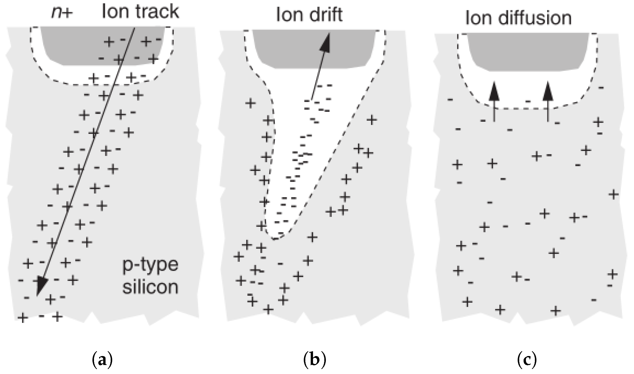
When a charged particle passes through the reversed biased PN junction of a transistor device, an SET fault is generated. The physical phenomena describing the fault can be divided into three main phases [
2], as presented in
Figure 1. Firstly, through the passage of the charged particle, the electrons in covalent bonds of the silicon crystal are ionized, as presented in
Figure 1a. The passage of the charge particle creates new electron–hole pairs, charge carriers, that would usually recombine, and no significant effect would be felt. However, due to the electric field present at the PN junction, the carriers are quickly captured before recombining, generating a drift current, as illustrated in
Figure 1b. Finally, an ion diffusion happens because of the carrier imbalance created on the junction due to the drift current, as presented in
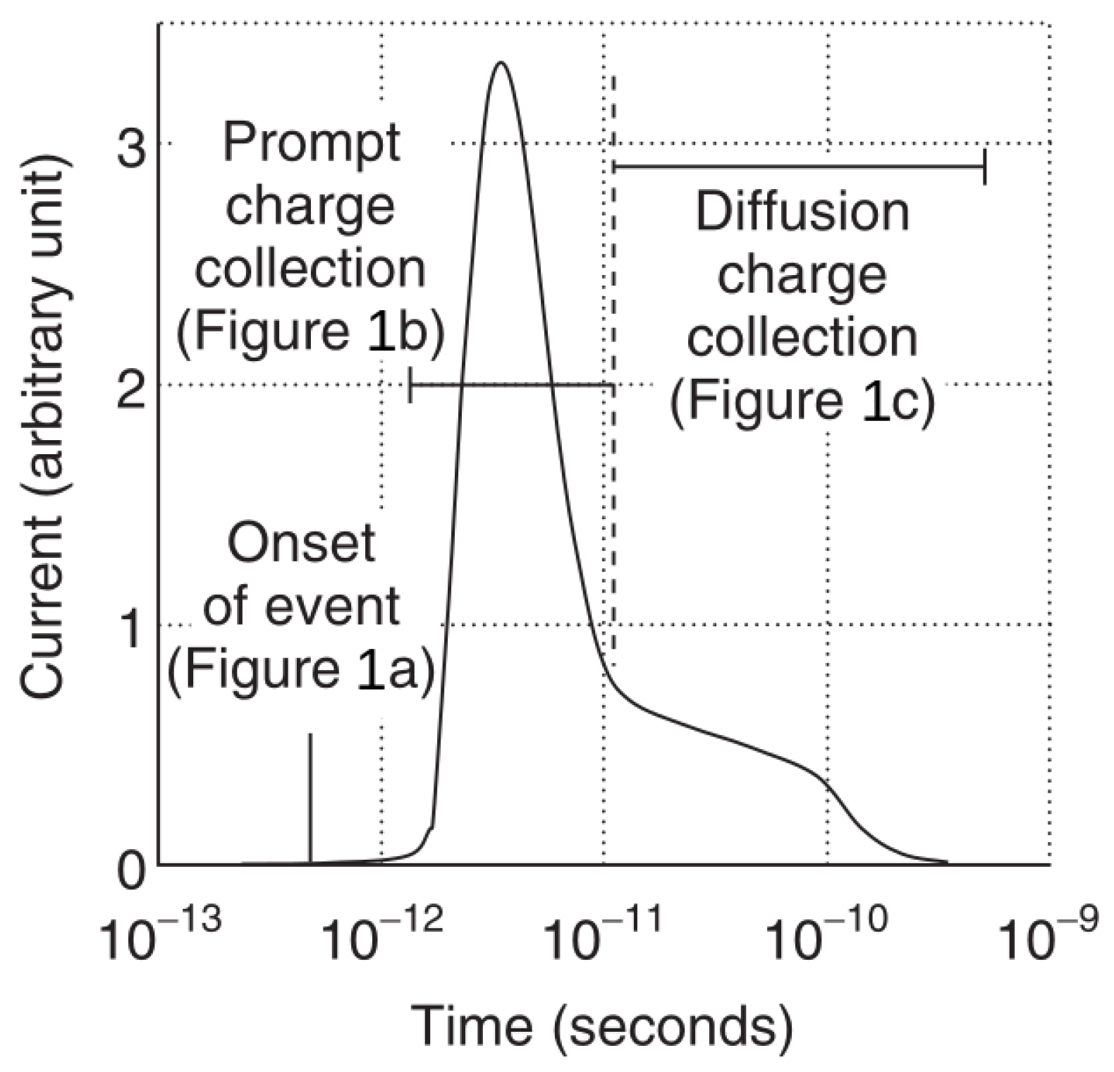
Figure 1c. It promotes the balancing of the charges and restores the device to normal behavior. The generated current is proportional to the charge collected by the transistor as the particle passes.
Figure 2 shows the shape of the generated current. Two distinct features can be observed: a high and ephemeral peak and a long plateau that, although not high in amplitude, persists for a relatively long time.
It is essential to distinguish between the two types of current pulses modeled. A SET fault can occur in both PMOS and NMOS devices, and faults have different behaviors in each. When the particle strikes the sensitive part of a PMOS, if the node is in a low logical state, it generates a low-to-high transition, characterizing a p-hit [
23]. Likewise, if the particle strikes an NMOS while it is in the high state, it generates a high-to-low transition, an n-hit.
There are several ways to simulate an SET [
24]. In this work, the electrical level simulation is used. Although not as precise as TCAD simulations, it can provide good results for circuits up to median size, with better precision and accuracy than RTL simulations.
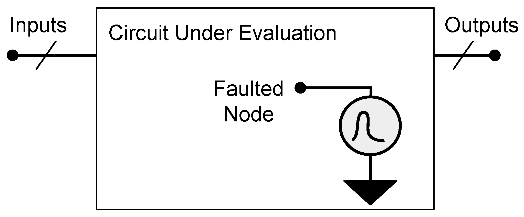
The geometry of the pulse should be configured in Quasar to explore different pulse models. In these approaches, the pulse is modeled as a current source. It is injected into the node to represent the current pulse generated by a fault that occurred in the devices connected to this particular node. This fault model is represented in
Figure 3, which illustrates the circuit under evaluation and the fault node insertion within its internal nodes.
One of the most accessible and straightforward approaches to simulate an SET at the electrical level is Messenger’s model [
25], a macro-model based on a single voltage-independent current source [
24]. The modeling of the transient current is given by Equations (
1)–(
3), where Q
COLL is the collected charge due to a radiation particle strike,
is the collection time constant of the junction, and
is the ion track establishment time constant, and
L is the charge collection depth, which decreases with the technology scaling. The empirical factor of 10.8 fC is derived from observations that, in bulk silicon devices, a typical charge collection depth is 2 μm for every linear energy transfer (LET) of 1 MeV cm
2/mg and an ionizing particle deposits about 10.8 fC charge along each micron of its track [
26,
27]. Equation (
4) presents the LET equation obtained from the previous equations. Equation (
2) shows the relation between the injected current (I(t)) and collected charge (Qcoll). As the default option on the Quasar tool, the collected charge timing constant (
) and timing constant used to establish the ion track (
) are set to 164 ps and 50 ps, respectively, according to [
26]. The charge collection depth (L) depends on the parameters of the technology. Furthermore, in a given simulation, all these parameters are set; both the LET and critical charge are dependent only on the fault current (I(t)).
Due to differences in the charge collection mechanism of FinFET devices [
28], the gate length of the fin should be adopted as the charge collection depth restriction. A comprehensive evaluation of the charge mechanism for FinFET devices is discussed in [
29], presenting various levels of differences in charge collection between NMOS and PMOS, which can influence the n-hit and p-hit of the evaluated circuits. Additionally, other studies indicate that the behavior of the current pulse in some cases resembles a double exponential source, followed by a longer hold period before it decays. In [
30], a TCAD evaluation is presented which obtained low-LET (LET of 1 MeV cm
2/mg) results, where the behavior of the curves is similar to that of the traditional double exponential curve. However, when considering a high LET (LET of 60 MeV cm
2/mg), the curve has a hold period before decay. Thus, it is important that the Quasar tool provides support to the user to define the different pulse geometries according to the particular conditions of each experiment.
Advances in technology have led to the development of new devices that address nanometer-scale effects. Multigate devices, such as FinFET, behave differently to planar CMOS devices due to their 3D structure [
5,
6]. The narrow vertical fin structure results in a smaller sensitive area for each device, changing the charge collection mechanism [
28,
31]. However, increasing the density of parallel fins to allow for discrete transistor sizing can increase the probability of a charged particle striking multiple fins placed closely together on the layout. Individually, a fin on FinFET devices has a lower critical charge than Planar CMOS of similar sizes; thus, multigate devices can have higher critical LETs overall due to their lower charge-collecting volume [
32]. Even with these changes in the charge collection mechanism, multigate devices remain sensitive to various energized particles in aero-spatial and Earth-level applications. Although the multigate devices have attractive properties to control the radiation-induced soft errors, other reliability challenges, such as process variability, can modify the linear energy transfer (LET) threshold to induce a soft error [
7].
3. Process Variability Effects
The scaling of transistors can present challenges for radiation-reliable systems. The impacts of scaling not only affect radiation robustness but also introduce high levels of process variability [
1]. Lithography, the fabrication process of microelectronic chips, faces various limitations as devices scale down. During device manufacturing, light is used to precisely interact with the material. At first, the most minor feature of the fabricated material was larger than the wavelength of the light used. However, this fact has changed, and at present the most minor feature of devices is significantly smaller than the wavelength of light used [
33]. Sub-wavelength lithography introduces greater variability in modern circuits due to the inherent imprecision of fabricating devices smaller than the wavelength of light used in the fabrication process. This variability impacts device behavior, such as on and off currents, and the main parameter this work is concerned with, the threshold voltage (V
th). The threshold voltage oscillation has a significant impact on radiation reliability, as a lower V
th allows a fault to propagate further throughout the circuit. During nanometer manufacturing, the primary sources of process variability are as follows:
Random Discrete Doping (RDD): The electrical properties of the PN junction are one of the most essential elements in the operation of semiconductors. The creation of the junction relies on the doping of other elements within the silicon lattice, changing the body type to either P or N. As transistors are scaled down to nanometric levels, the number of atoms in a transistor channel reaches about 100 or lower [
34], and dopant atoms are still decreasing in number as the transistor continues to scale down. The reduced number of atoms reaches a point where they can be counted as discrete, introducing uncertainty regarding the exact number of doping atoms that were inserted. Thus, the process becomes subject to variability. RDD has a significant impact on modern transistors, as the absence or inclusion of a single atom accounts for a substantial portion of the channel doping. In planar CMOS devices, this is one of the primary factors determining the threshold voltage (V
th) of the transistor channel.
Metal Gate Granularity (MGG): The silicon lattice that composes semiconductors is not always perfect. This crystalline structure can vary, with some instances where a device has a higher granularity than other devices. This factor is especially important in the silicon-to-metal interface on the gate of transistor devices, comprising the MGG.
Figure 4 presents a diagram of the interface and illustrates how the MGG of a real device differs from that of an ideal one. Its variation impacts the work function (WF) of the device, requiring more or less energy to free an electron from the material, which allows for conductance and significantly affects the V
th of a device [
35]. In FinFETs and other multi-gate devices, the MGG, and thus the work–function fluctuation (WFF), is much more impactful than RDD, as these devices have low-doped channels [
36,
37].
The impact of process-induced variability on the electrical behavior of FinFET-based PFET and NFET transistors was comprehensively analyzed for predictive technology nodes ranging from 20 nm to 7 nm [
35]. Among the key parameters affected by process variations, gate length and fin thickness exhibit substantial deviations from nominal values, while fin height presents comparatively low variability. However, the work–function fluctuation (WFF) is shown to be the primary source of variability, impacting both the ON and OFF currents. The WFF alters the expected behavior of the threshold voltage, introducing a significant variation in static power consumption. In standard cells, increased WFF sensitivity results in a wide dispersion of leakage currents. The significance of WFF is also validated through 3D TCAD simulations in 14 nm FinFETs [
38]. These studies demonstrate that reducing the average metal grain size from 10 nm to 5 nm results in a nearly linear decrease in threshold voltage standard deviation, with reductions in variability reaching 45%.
Soft error tolerance, particularly single-event transients (SETs), has also been analyzed in the presence of process variability [
39,
40,
41,
42]. Using the MUSCA SEP3 predictive tool [
39], validated using TCAD-based mixed-mode simulations, accurate evaluations of SET susceptibility were performed for FinFET-based logic gates. The results highlight that process variations can exacerbate the sensitivity of nodes to ionizing particles, potentially increasing soft error rates in critical logic structures.
Radiation and process variability effects present reliability challenges in advanced FinFET technologies [
7]. These effects manifest not only in electrical performance, i.e, as a degradation in delay and power consumption, but also in the resilience of logic cells under environmental and radiation-induced faults. The interaction between process variation and fault mechanisms underscores the need for robust design methodologies that integrate variability-aware analysis and radiation-hardening strategies to ensure reliable operation across nanometer technology challenges [
43].
4. Quasar Tool Concepts and Development
Quasar’s primary objective is to provide a straightforward and user-friendly method for designers to characterize a circuit’s radiation response automatically. It automatically determines how an SET fault can cause an error and determines robustness metrics, such as the minimal LET for every relevant configuration in which a fault can occur. It also fully automates a method for evaluating the impact of variability in the radiation response of a circuit, outputting graphs that plot this relationship.
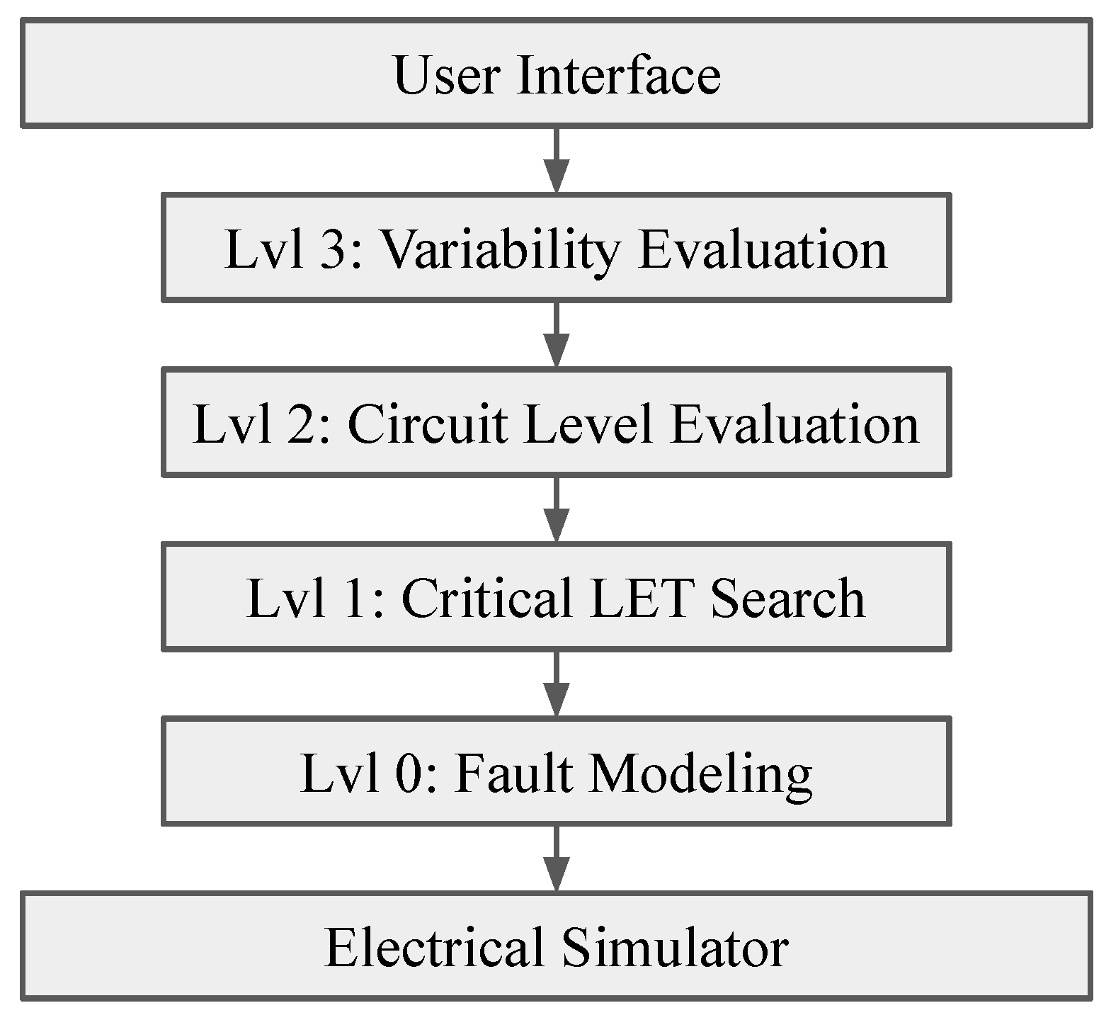
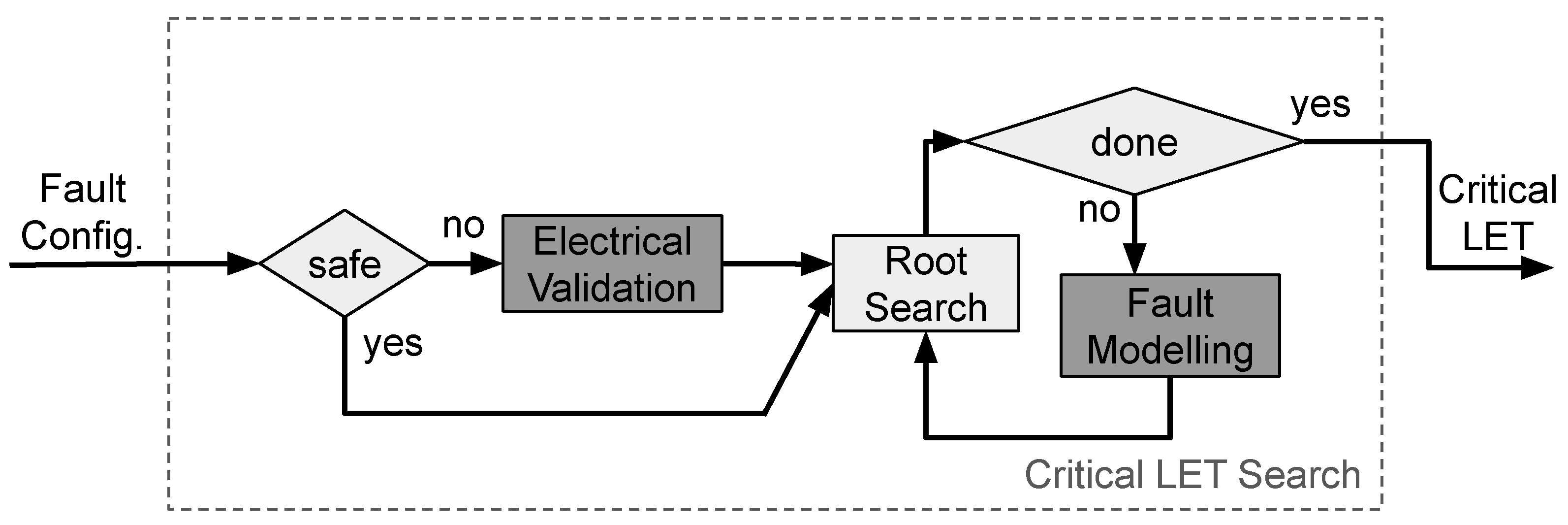
Figure 5 presents an overview of the layer model adopted in the Quasar development. It has four layers of abstraction: Layer 0, Fault Modeling, makes a single call to the electrical simulator and simulates a single SET fault; Layer 1, Critical LET Search, makes multiple serial calls to layer 0 to determine the minimal LET of a given SET configuration; Layer 2, Circuit-Level Evaluation, makes multiple parallel calls to layer 1 to gather all the minimal LETs of all SET configurations of a circuit, thus gathering all minimal LET
th of the circuit; Layer 3, Variability Evaluation, makes multiple parallel calls to layer 2 to determine the LET
th of a given circuit under certain variable parameters and integrates these with a predictor model to speed up the simulations. The development and concepts adopted in each layer are presented in the following sections.
The development of Quasar is integrated with a SPICE simulator to facilitate electrical-level simulation, providing a user interface for comprehensive circuit evaluations. It can currently be integrated with two electrical simulators: NGSPICE version 44, an open-source electrical simulator, and Synopsys HSPICE® version T-2022.06-SP2. In addition, the implementation is independent of a specific transistor model or type. The tool is fully implemented in the Python version 3.8.10 language, using mainly an object-oriented approach.
4.1. Layer 0—SET Modeling
For an SET fault to create an error, the current pulse generated on the faulted node has to propagate with significant amplitude to an output interface. Therefore, the abstraction created by this layer is a function that takes the faulted node, the output interface, the current pulse, and the circuit input vector as the input, and then returns the minimum/maximum voltage in the output interface, depending on whether it was in a high/low logic state, respectively.
The SET fault’s current pulse is generated by a double exponential current source inserted between the faulted node and the ground (gnd) node, as described in
Section 2. This layer provides no guarantee that the fault will not be masked in any way.
One SET fault insertion and propagation is completed within a single electrical simulation. The vast majority of simulator calls in Quasar simulate an SET, and the number of simulations is considered the main bottleneck of performance. Most optimizations aim to reduce the total number of simulations, which can reach hundreds of thousands in some cases. Internally, Quasar works with the value of the pulse’s current, only converting it to the critical charge and LET results at the end of the process.
4.2. Layer 1—Critical LET Search
This layer is responsible for finding the minimal LET an SET needs to create an error at the output; that is, to not be electrically masked. It inputs a fault configuration, which includes the faulted node, output interface, and circuit state as inputs, and outputs the minimal current necessary to cause a bit flip at the output. We define a bit flip to have occurred when the output voltage is halfway between VDD and GND.
4.2.1. Electrical Validation
Before determining the critical LET of a fault configuration, it is important to determine if this configuration is logically masked. During the calling of this layer, it is possible to determine if a fault configuration is safe; that is, not logically masked. If this does not happen, before searching for the critical LET, logical masking is determined electrically. It means two extra simulations have to be carried out: (1) to obtain the logic state of both the faulted node and output, information that is known beforehand in the safe case, and (2) to verify logical masking. Achieving the latter is accomplished by injecting an extremely high current pulse into the faulted node. If no change is detected at the output interface, there is logical masking, the configuration is invalid, and the Critical LET Search stops returning a null LET.
4.2.2. Critical LET Search
With the validity of the configuration confirmed, a search for the critical LET is conducted. The search takes into consideration the output voltage response to transient faults. The search is conducted for a fixed fault configuration. It utilizes the abstraction provided by the Set Modeling layer to represent the entire electrical response simulation as a function that takes a current as input and yields a voltage as output, as presented in Equation (
5).
Figure 6 shows a simplified overview of the Critical LET Search process. Boxes in dark gray represent the calling of a previous layer.
As the objective of the LET Search is to find the current value that makes the output voltage equal to half the supply voltage, this value is subtracted from the output, so the target voltage is 0. This makes the target value the root of the function.
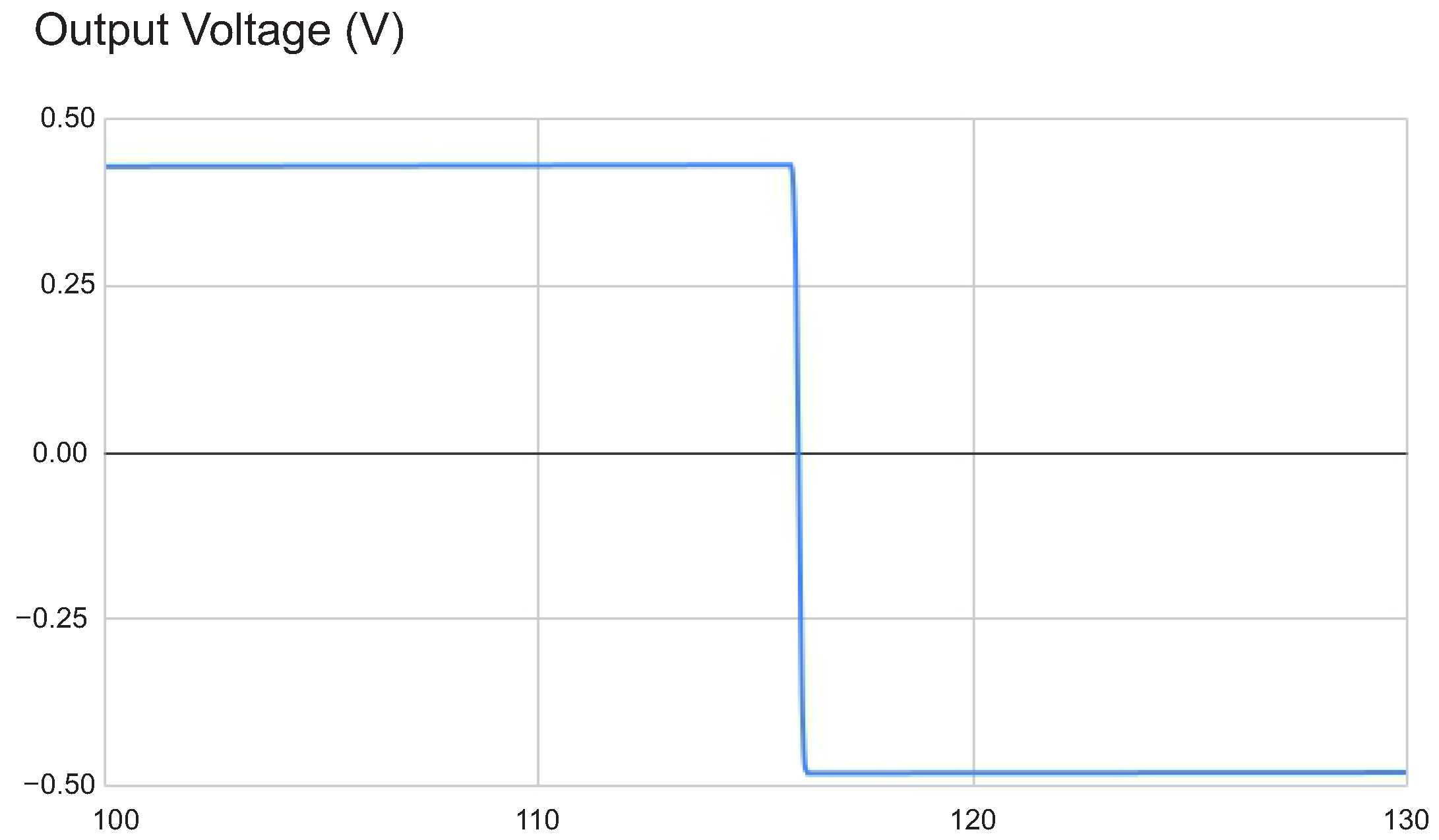
For a valid fault configuration, the shape of this function resembles a step, as shown in
Figure 7. This occurs because, for low current values, the fault is electrically masked, resulting in no change to the nominal output voltage value. For sufficiently high currents, the fault propagates with sufficient intensity and width, causing the output voltage to be completely inverted.
Despite a tiny current fluctuation, the overall function is monotonic, either increasing or decreasing depending on the nominal output voltage.
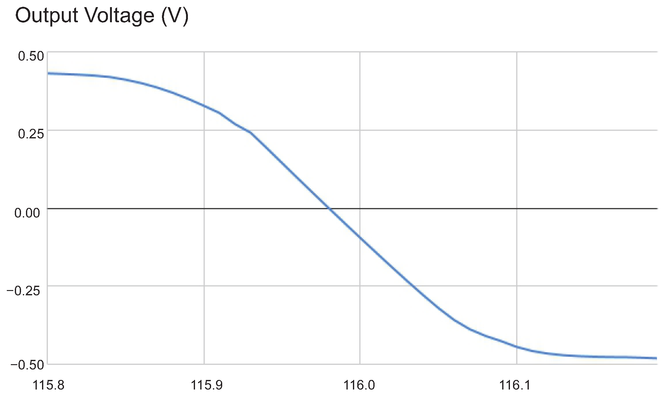
Figure 8 shows a zoom-in on the transition zone of the function of
Figure 7. This sigmoidal shape is favorable for root searching as it approximates a linear function at the root.
Two different root search approaches were investigated. Both the classical Bisection and False Position algorithms were tested. Three circuits were used as benchmarks of performance—the Mirror Full Adder, ISCAS85 C17 [
44], and the NAND2 gate—all implemented with the 7 nm ASAP7 node [
45], adopting three fins in every transistor. The precision of the search demands an output voltage within 1 mv, and the bounds of the search started at 100 and 200 nA, and were expanded if needed.
Table 1 shows the number of simulations per distinct fault configuration. If two fault configurations have the same faulted node, propagated output, and current value, and different input states, they are considered to be the same fault configuration by the tool, and only one of the input states will be simulated; its result will be considered for the others.
False Position consistently gives better results than Bisection. Due to the function shape, both methods behave the same until the search space reaches the transition zone. Once within the transition zone, False Position exploits the linearity of the zone, which Bisection does not, thus making it converge faster.
In the best case, the number of simulations per configuration would be exactly one. If the current value were predicted, only a single simulation would be needed to confirm the value. In the case where the bounds start within the transition zone, two simulations are required to establish the bounds. The algorithm can determine the root, and a third simulation is needed to confirm this.
4.3. Layer 2—Circuit-Level Evaluation
The LETth of a circuit is defined as the minimal LET necessary to cause a bit flip in an output interface in the most sensitive fault configuration. To find the LETth, every valid fault configuration has to be considered. Thus, this layer’s responsibility is to find the LETth. It is possible to generate every combination of factors that comprise the fault configuration and allow the Critical LET Search to determine its validity electrically. However, this is not ideal, as the main performance bottleneck is the number of electrical simulations. In electrical validation, two extra simulations are carried out for every possible fault configuration. As an illustration, a test was run using the default parameters of the search for the minimum LET, with a Mirror Full Adder as a benchmark. It was observed that, with this method, 41% of all simulations were only used for validating fault configurations.
Firstly, there is a simple filter to discard impossible faults. If a node is not connected to a terminal of a PMOS device, it cannot undergo a 0-1-0 fault; likewise, the same is true for NMOS and 1-0-1 [
23]. Thus, every fault configuration with these properties can be discarded before any further consideration. To avoid unneeded electrical validation, a logical validation of all fault configurations is conducted before any electrical simulation.
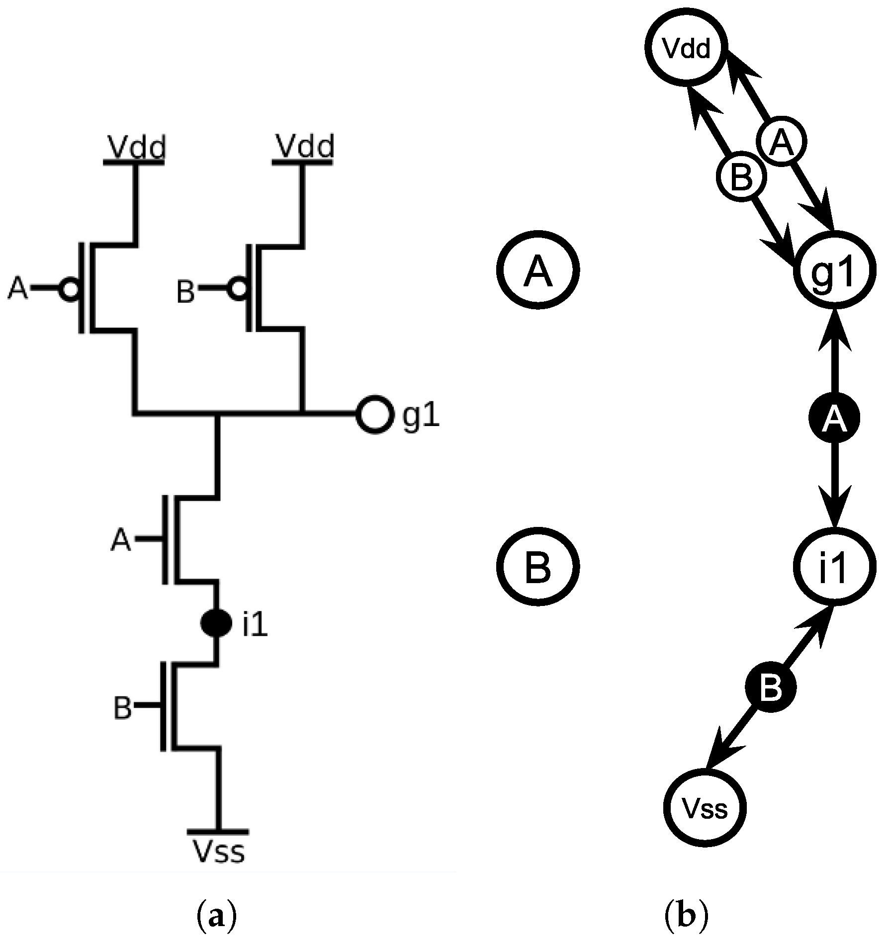
To logically validate an SET fault, the circuit is modeled as a logical graph. Every electrical node is modeled as a Boolean node, and for every transistor, an undirected edge is created between both terminals (source and drain). This edge has a Boolean state that indicates whether it conducts, depending on the control node’s state.
Figure 9 shows the circuit and the graph model for a NAND2 gate. The circle in the middle of each edge indicates which node’s state controls conduction. A white/black circle indicates that it conducts when the control node is in a low/high logic state, but not in the high/low state, respectively.
Figure 10 shows the flow of this layer: it inputs a circuit and outputs all valid configurations along with their respective minimal LETs, which are named the circuit’s radiation profile.
When the graph is built, all possible fault configurations are modeled. In order for the simulation to be correct, it is necessary that, for every transistor, the state of its gate is determined before the states of its terminals. The following model assures this fact.
The first step in the simulation is to split the graph into Electrical Path Groups (EPG). An EPG is defined as a group of nodes that connect through source/drain terminals of a transistor, so there is an electrical path from every node of the group to every other node, even if the path is not conducting. Voltage sources are not considered in this definition and do not belong to any EPG.
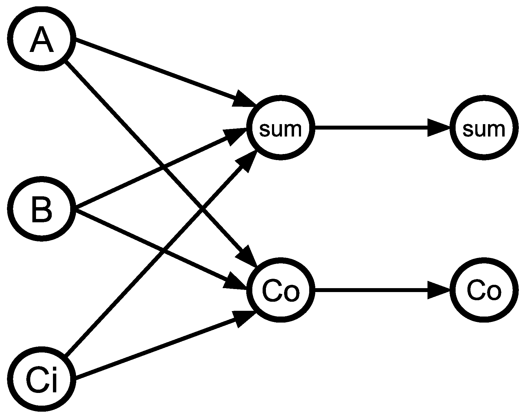
Figure 11 shows the graph model of a classical Mirror Full Adder; some node names were omitted to avoid visual pollution, and voltage source nodes were replicated as they do not belong to any group. In the graph, these EPGs can be visually identified by the seven disjoint subgraphs.
Another graph with a node representing each EPG is created. For every transistor in the circuit, an arc is created, going from the group containing the gate node to the group containing the source and drain nodes. For the Mirror Full Adder example, the results in the graph are shown in
Figure 12, where each EPG is labeled with the name of one node in it. In the EPG graph, a Topological Sorting algorithm is run to provide the order in which the EPGs will be logically simulated. This order is crucial, as it ensures that the logical state of every transistor’s gate is determined before the states of its source and drain are even considered. If sorting cannot be carried out, there will be no logical validation; all fault configurations will be marked as unsafe and electrically validated.
If an order is possible, all fault configurations will be modeled in the original circuit graph. Every node’s logical value is set to undefined, except for voltage supply and input nodes, which are set according to their logical values. Then, for each EPG, the logical signal propagates from these nodes. At the end of the logical simulation, the logical value for every node is known.
Algorithm 1 presents the process used to set all logical values in an EPG. It begins with a list of all nodes that already have a known value and then runs a depth-first search. It takes the node on top of the stack and propagates its signal through every conducting transistor that has a drain/source connected to it, adding this to the search list. By the end, every node in the EPG will have an appropriate logical value.
To simulate a fault, every EPG starting from the faulted one will be simulated again. The faulted EPG will run Algorithm 1 with the faulted node starting on top of the stack with a set value. This ensures that it will propagate its signal to every possible node before other signal sources are considered. This is important because when considering an arbitrarily large fault, its signal will have priority in propagating. When the entire circuit is simulated, if an output has a different logical value than its original, the fault is propagated to this output, indicating that the fault configuration is valid. Every fault configuration is tested in this way. Finally, all valid configurations are cached, so if another circuit-level evaluation is carried out for the same circuit, the configurations are known beforehand. As the Critical LET Search of the fault configuration is independent, this is performed in parallel.
| Algorithm 1 Logical Propagation Through an Electrical Path Group |
| 1: | function SetLogic(EPG, faultedNode) |
| 2: | Input: Electrical Path Group (EPG), faulted node |
| 3: | Output: Logic states propagated through the EPG |
| | // Transistor(node): returns all nodes reachable from ‘node’ via a single transistor
// Conducting(transistor): returns true if transistor’s control node enables conduction
// LogicState(node): returns the logic state of a node |
| 4: | begin |
| 5: | {vdd, gnd, faultedNode} |
| 6: | |
| 7: | while not Empty() do |
| 8: | PopBack() |
| 9: | if then |
| 10: | continue |
| 11: | end if |
| 12: | Add to |
| 13: | for each in Transistor() do |
| 14: | if not Conducting() then |
| 15: | continue |
| 16: | end if |
| 17: | OtherNode(, ) |
| 18: | if then |
| 19: | continue |
| 20: | end if |
| 21: | SetLogicState(, LogicState()) |
| 22: | InsertBack(, ) |
| 23: | end for |
| 24: | end while |
| 25: | end |
4.4. Layer 3—Variability Evaluation
This layer is responsible for characterizing the impact of variability on the radiation robustness of a circuit. Firstly, the variability parameters are defined. One or more physical attributes of a transistor model are selected based on the variability effects in the specific technology. A distribution of these parameters is created, generally a Gaussian. For each point in the distribution, a complete circuit-level evaluation will be done. The final data is gathered, and a simple automatic analysis is generated. A view of the operation of Variability Evaluation is presented in
Figure 13.
The nominal value of this parameter is taken as the mean value of the distribution. A percentage and sigma () values are inserted to generate a standard deviation.
A complete circuit-level evaluation can involve hundreds of simulations. This becomes a problem in variability evaluation, in which thousands of different points can be evaluated [
7,
35,
39]. To accelerate convergence, a prediction algorithm is implemented to enhance the efficiency of the Critical LET Search.
All Critical LET Searches seek the root situated on the transition zone of the fault function. Typically, all searches start from a standard bound; however, with an estimate of where the root of the function is, a narrower bound centered on the estimate can be used to initiate the search. This causes the search to converge in fewer iterations, i.e., fewer simulations are used if the initial estimation is correct.
Quasar implements an estimation tool that builds its model concurrently using the simulations of the Critical LET Search. A separate model is built for each distinct fault configuration. When a Critical Let Search starts, it requests an estimation from the prediction model and uses this as the starting bounds of the search. When the search converges, it sends its result to the model, allowing it to consider that data point and make more accurate estimations for subsequent calls.
The function that the model tries to predict has the physical parameters that are changed in the variability evaluation as input, and returns the minimal current necessary to propagate a fault.
Figure 14 shows the distribution of points one of these functions might have. In the tested cases, a physical parameter, such as the WF, is considered, and its distribution is applied to both NMOS and PMOS devices. The studied functions have insignificant noise, are relatively smooth, and are nearly monotonic. Given these properties, the k-nearest neighbors (k-NN) regression approach was chosen, as this works well with the aforementioned characteristics of the function [
46]. We specifically used the euclidean distance-weighted 3 NN from the Scikit-learn Python module [
47], using the physical parameters that are changed in the variability evaluation as input. Whenever a prediction is called, the three closest points to the desired prediction are gathered. We take a weighted average of the current values of these three points, where the weights are inversely proportional to the distance the point is from the predicted point.
Table 2 shows the average number of simulations per fault configuration on different prediction methods. The same circuits from
Table 1 were used. For each case, a variability analysis was performed using 2000 points. An average method was also compared. Whenever a prediction was requested, the answer was simply the average of all the current values in the model.
The average prediction method starts the Critical Let Search from a more informed value than the arbitrary 150 that is the default. This, on average, reduces the number of simulations per fault configuration by 1. The k-NN method presents a significantly greater gain, reducing the number of simulations by about half, which implies a speed-up of 2 in the complete variability evaluation.
Furthermore, as previously discussed in the critical LET search, the lowest possible number of simulations per fault configuration is one if the prediction is exact. If the prediction misses the exact value, one iteration of the root search is performed, totaling three simulations: one for the initial guess, another to determine the inclination of the transition zone, and a final one to find the root. We observe that for the NAND2 gate, the k-NN algorithm yields a result below this threshold, indicating that, on average, the prediction is accurate.
4.5. Final Remarks
The Quasar Tool was developed following open-source principles, and the current version is available at [
48]. Its modular architecture ensures its easy integration with other electrical simulators and adaptability to different technological requirements. PVT (process, voltage, temperature) analysis is critical for integrated circuit design, as variability directly impacts circuit robustness, especially against radiation-induced faults in bulk CMOS technologies [
3]. For instance, temperature variations alone can increase radiation susceptibility by up to 50%. In this way, Quasar already supports a detailed variability analysis (e.g., by modifying the SPICE descriptions for temperature ranges or voltage points). To further accelerate the PVT variability assessment, a dedicated combined functionality is under development in Quasar.
Machine learning has emerged as a powerful approach to accelerate single-event effect analysis, with several promising methodologies demonstrated in the recent literature. Ref. [
49] developed a neural network-based SET pulse current model that achieves a significant speed-up compared to TCAD simulations while maintaining accuracy in its circuit-level implementation. Similarly, ref. [
50] proposed a learning-based structural regression method that efficiently models SET propagation in both CMOS and Pass Transistor Logic circuits, enabling analysis without the need for exhaustive simulations. For SET identification, ref. [
51] demonstrated an automated approach combining ionizing radiation effects spectroscopy with machine learning (kNN algorithm) to classify transient events based on statistical features. These works collectively demonstrate that ML techniques can substantially reduce computational overhead while maintaining accuracy in their analysis, highlighting their importance for future exploration. In subsequent versions of Quasar, we plan to incorporate dedicated modules to enhance SET analysis by integrating these machine learning approaches.
5. Results
Even during the development stages of the Quasar tool, preliminary versions were adopted to help in gate-level and transistor-level circuit evaluations regarding radiation robustness and process variability impact [
52,
53]. To demonstrate Quasar’s usability and how it can provide further insight to circuit design, four radiation robustness case studies are presented. The first one presents a transistor-level evaluation, demonstrating how the developed tool facilitates an analysis of the impact of pull-up and pull-down networks on radiation robustness. The second case study presents an evaluation of an XOR2 gate under process, voltage, and temperature (PVT) variability, considering statistical evaluations adopting the 32 nm bulk CMOS predictive model [
54]. The third one presents a gate-level evaluation to illustrate how gate-mapping affects radiation robustness, considering process variability [
52]. The process variability in the first and third experiments considers that all circuits were implemented in 7 nm ASAP PDK [
45]. We set up Quasar to run 2000 points for the variability analysis, using WF as the variability parameter with a Gaussian distribution of 3
and a 5% standard deviation [
35]. The results generated by Quasar are presented in table formats and also in scatter plots. Finally, the last case study compares the Quasar methodology with related work [
55], presenting a comparison between the circuit results generated for different technology nodes.
The set of case studies presented here indicates the utility and versatility of Quasar when analyzing radiation robustness. Furthermore, it demonstrates why variability can be a crucial factor in evaluating circuit reliability, underscoring the importance of the tool’s variability feature.
5.1. Restoring Network Case Study
This case study has two main objectives: (1) show how Quasar can provide insight into circuit reliability under radiation at a transistor level; (2) explain the different behaviors of the NAND2 and NOR2 gates under WF fluctuations. For this purpose, an analysis of the Inverter, NOR, and NAND gates was carried out. The functions NOR and NAND were considered, with two to four inputs. All circuits were implemented using a 7 nm model from ASAP PDK [
45] with minimal sizing.
Figure 15 shows the topology for the NAND2, NOR2, and Inverter gates.
Table 3 shows the main statistics for the three logic gates regarding radiation sensitivity, observing the LET
th of the circuits without considering process variability in the Nominal column, and the distribution of the results considering process variability using the Mean (
), standard deviation (
), minimum (Min) and maximum (Max) values. It is possible to observe that the inverter has a restoring structure that elevates the charge collection demand to provoke a failure output. However, the process variability evaluation indicates that there may be situations where the required threshold drops dramatically, to nearly 21 MeVcm
2/mg, about 21% of the expected robustness at nominal conditions, i.e, without process variability. The NOR2 is about 27% less robust to SET than the NAND2. These results suggest that logic function refactoring, exploring more NAND2, could improve circuit robustness, considering the nominal process behavior. However, process variability can affect this NAND2 superiority.
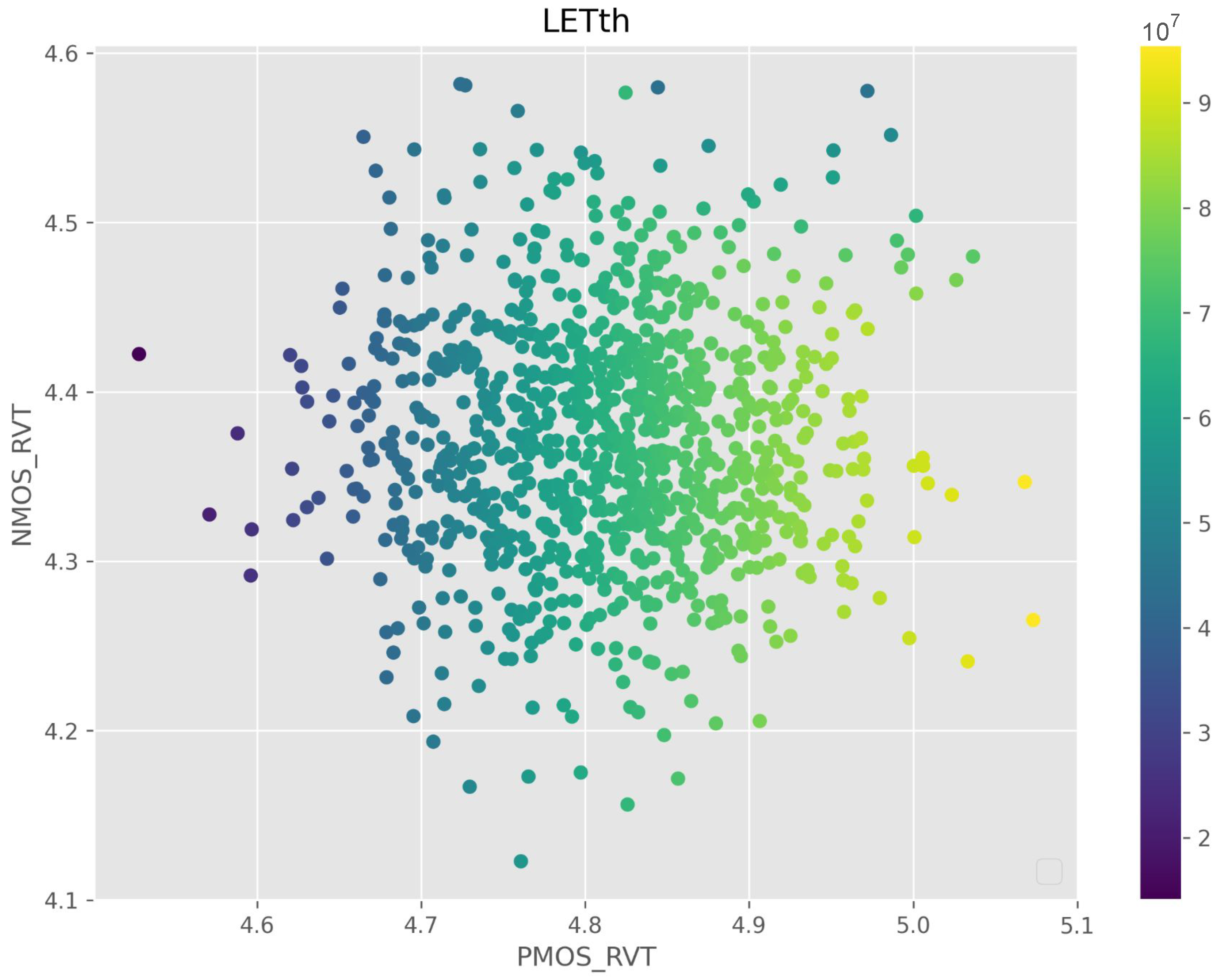
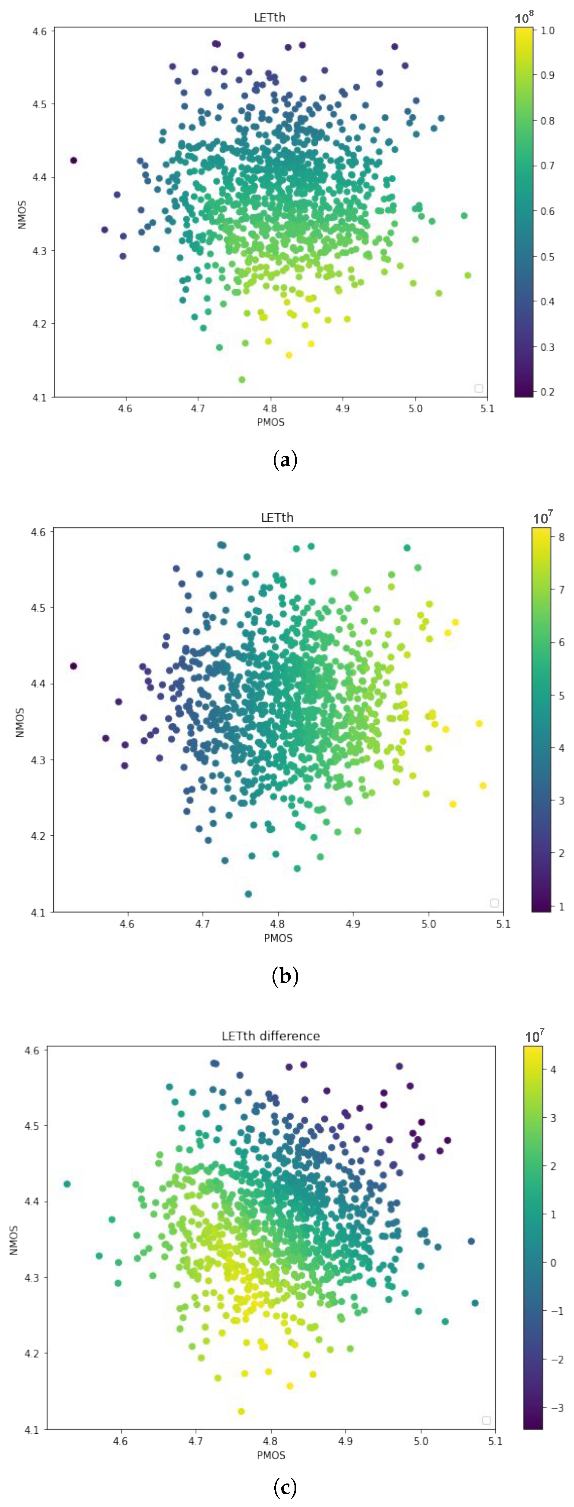
Figure 16a and
Figure 16b detail the LET
th dispersion of both the NAND2 and NOR2 gates under WF fluctuations, respectively. Although, overall, the NAND2 gate is the more robust of the two, they have different responses to each device fluctuation. While the NAND2 robustness responds to variations in both the NMOS and PMOS WF fluctuations, the variation in the former has a greater impact than variations in the latter. For the NOR2, the variations in NMOS are insignificant compared to those in PMOS. Moreover, the most robust WF configuration of both gates is not the same. This motivates a comparison between the two, considering each point.
Figure 16c shows the difference between the LET
th of the NAND2 and NOR2 gates at each point. Notably, the dispersion reached negative values in some configurations of the devices’ WFF, indicating that, in those cases, the NOR2 gate is the most robust version.
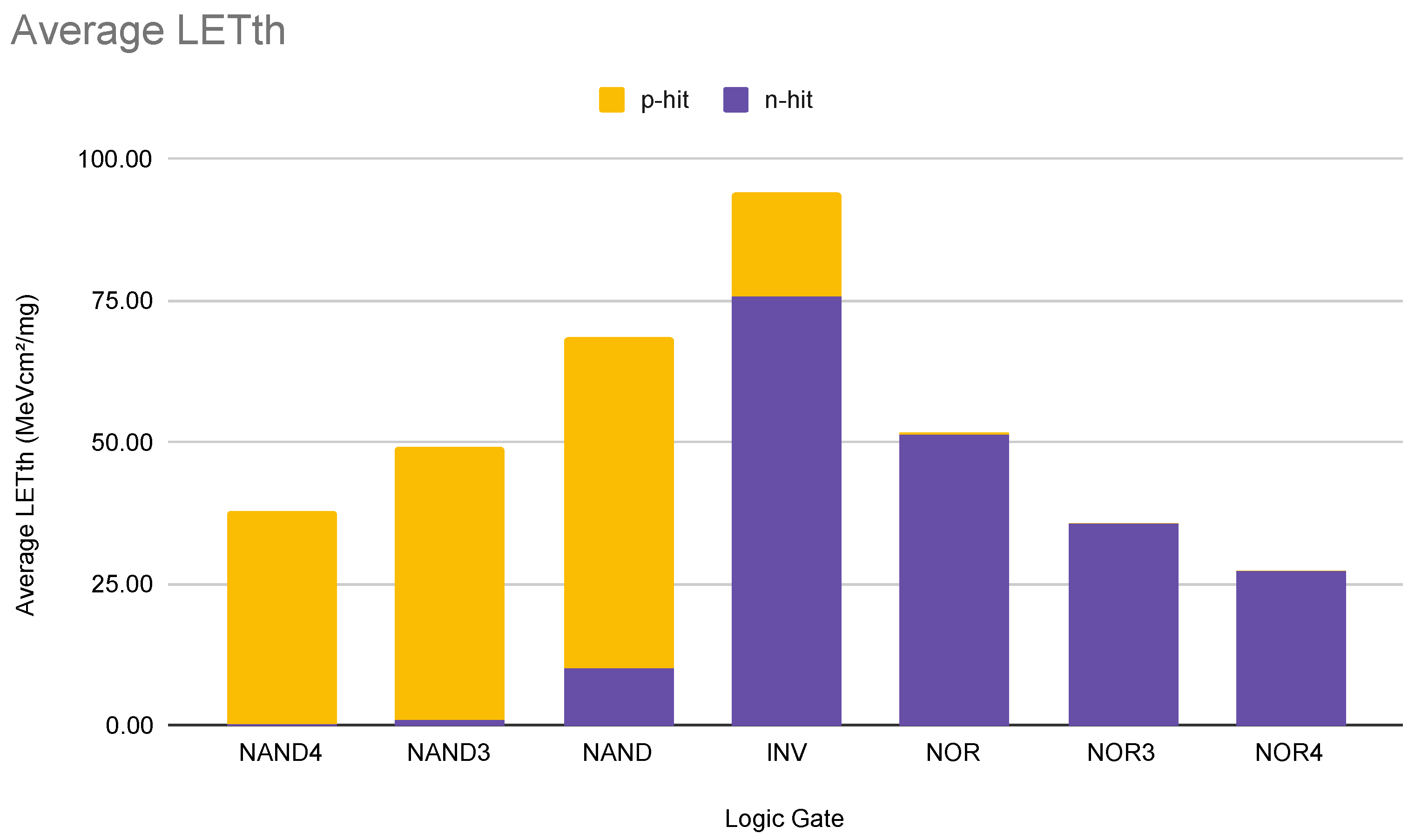
An additional evaluation examines the impact of p-hit and n-hit on the basic gates.
Figure 17 shows a plot of the average LET
th of the gates analyzed. For each gate, the vast majority of the critical nodes in the distribution correspond to the circuit output. Each bar in the graphic shows the proportion of pulse types of the distribution, either p-hit or n-hit. In both the NAND and NOR functions, as the number of inputs increases, the gates become less robust to changes in the input values. It is also observed that for the majority of the NAND cells, the n-hit is the critical pulse while the p-hit is the critical pulse for the NOR function. Both these facts are due to the same reason: the path-restoring currents take in the critical fault configuration.
When charge is collected/depleted during an SET, it needs to be discharged/restored. A current needs to flow between the faulted node and either the ground or the supply node, depending on the charge type. Therefore, in most cases, the critical fault configuration will be the one that causes the restoring current to take the path of most resistance. This means the charge takes longer to be depleted/restored, and hence needs less charge to propagate a fault. In nominal conditions, for every gate of both NAND and NOR functions, this occurs when the restoring current needs to pass through the serial network, e.g., when a NAND2 gate has both inputs at a high level, meaning that a fault at the output gate needs to be restored though a current that passes through the NMOS network.
Furthermore, as the gate input number increases, the number of devices in the serial arrangement also increases, weakening restoring currents and increasing sensitivity. Additionally, the NAND/NOR function is more dependent on NMOS/PMOS variability, respectively, because these are the transistors in its series network. The rare cases where this does not apply occur only in extreme situations, where, due to WF fluctuations, the conductance of the series network transistor is very high. In contrast, the conductance of the parallel network is very low. Thus, the parallel network will present a lower resistance than the series network.
5.2. PVT Evaluation of XOR2
A second experiment was conducted to demonstrate the versatility of Quasar in comparison to other technologies, including process, voltage, and temperature evaluations, as well as the potential for statistical manipulation of the data generated by the Quasar tool used for this analysis.
Devices in this experiment, we adopted a classical CMOS topology of a XOR2 gate, presented in
Figure 18, composed of eight transistors. The inputs and internal nodes were named, and these names were adopted in the further evaluation. This cell requires both the input and complementary input to compute the XOR function. The inverters to compute the complementary input are described together with the cell, but were omitted in the cell evaluation. The technology node used in this experiment is the 32 nm bulk CMOS predictive node [
54]. The devices were sized according to logical effort and the difference in mobility between the PMOS and NMOS bulk devices. The nominal voltage of this technology was 0.9 V. The experiments considered the impact of process, temperature, and voltage variability on the current adopted in the simulation to determine the critical LETth. The fault current is a double exponential that follows the definition in Equations (
1)–(
4). Thus, a lower current is more critical to the robustness of the circuit, and a higher current indicates more robustness. The variability was simulated by considering threshold voltage variability as a Gaussian distribution with a 3
standard deviation and 10% of the standard deviation for NMOS and PMOS devices, using 2000 Monte Carlo runs. The temperature oscillated in the range of 0 °C to 125 °C, in steps of 25 °C. Furthermore, the voltage fluctuations were considered to be within +/− 10% of the nominal voltage. These parameters are usually set in this range for standard cell library characterizations. However, all these parameters can be set by the Quasar user according to the application and experiment requirements.
Based on the log generated by the Quasar tool for process variability evaluation, the data generated for each fault case describe the node, output, n-hit versus p-hit fault, the PMOS threshold voltage, the NMOS threshold voltage, and the fault current (I(t)) that provoke unexpected behavior at the output of the cell, i.e., identify a faulty condition, for each run of the Monte Carlo. These data are passed to a statistical evaluation adopting Python functions. We show the Histogram, boxplot, and density curve in
Figure 19 for the current behavior. It is possible to see that the current follows a bimodal distribution. This bimodality is a key characteristic, indicating that the current values are not uniformly distributed but rather cluster around two different levels. The boxplot further confirms the spread and identifies potential outliers at both ends, which could correspond to extreme values within these two underlying groups. Understanding this bimodal nature is crucial for any further analysis or modeling, as it implies that a single average or standard deviation might not fully capture the behavior of the current variable. The individual evaluation of the SET sensitivity under process variability for each node of the XOR2 cell provides a complementary insight into this bimodal behavior, revealing two distinct clusters of nodes: the most sensitive and the most robust. To discuss this,
Table 4 and
Table 5 present more detailed data about each node’s behavior.
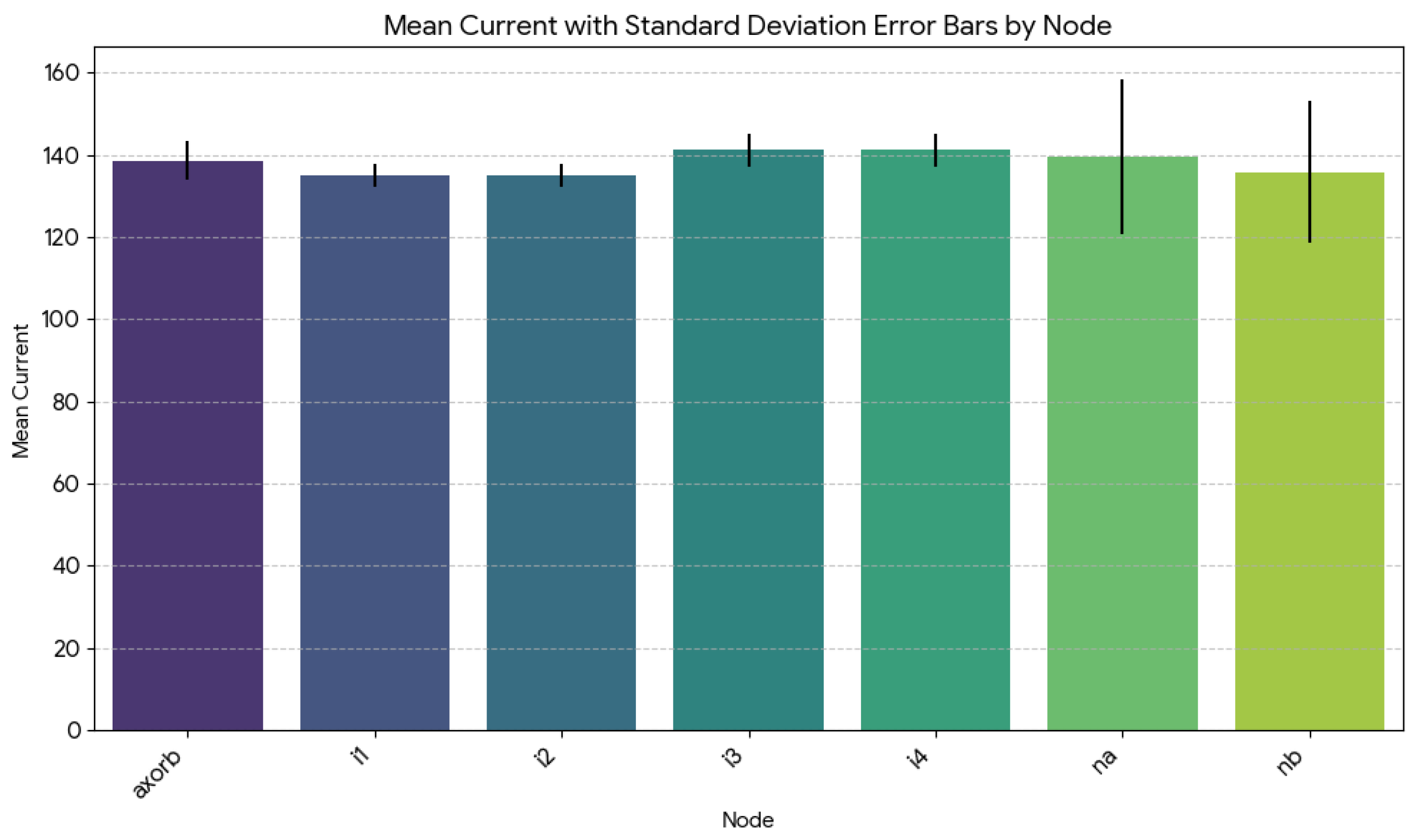
Observing the results for the process variability impact on the robustness of the evaluated XOR2 cell, we will consider, for each node of the circuit, the mean current and its respective 95% confidence intervals (CI), as shown in
Table 5, and discuss the current levels concerning each node.
The nodes with a lower mean and CI are, from the most sensitive to more robust, nodes , , and . Nodes and presented very similar sensitivities, with a mean current and CI in the same order (: mean = 134.95, with a CI from 134.83 to 135.07, : mean = 134.96; CI from 134.85 to 135.08). These two nodes are the critical nodes among all the XOR2-evaluated nodes. The confidence interval is also very tight and on the lower end of the spectrum, suggesting that the current values for and are consistently low. The node (mean: 135.90; CI: 135.36–136.43) is slightly more robust than and ; however, remains in the lower current range. Its confidence interval is wider than and , suggesting more variability, but its mean remains relatively low, indicating it could also be a critical node.
Nodes and show the highest mean current values, with confidence intervals that are relatively narrow and firmly in the higher range, indicating that these nodes consistently exhibit a more robust behavior level.
Node
demands deeper discussion. These node results fall within the higher current range, making them relatively robust. However, it is worth noting that their standard deviation, as presented in
Table 4, was significantly higher than that of the other nodes, suggesting greater dispersion in their robustness.
Figure 20 presents the mean current, with standard deviation error bars for each node of the XOR2 cell evaluated.
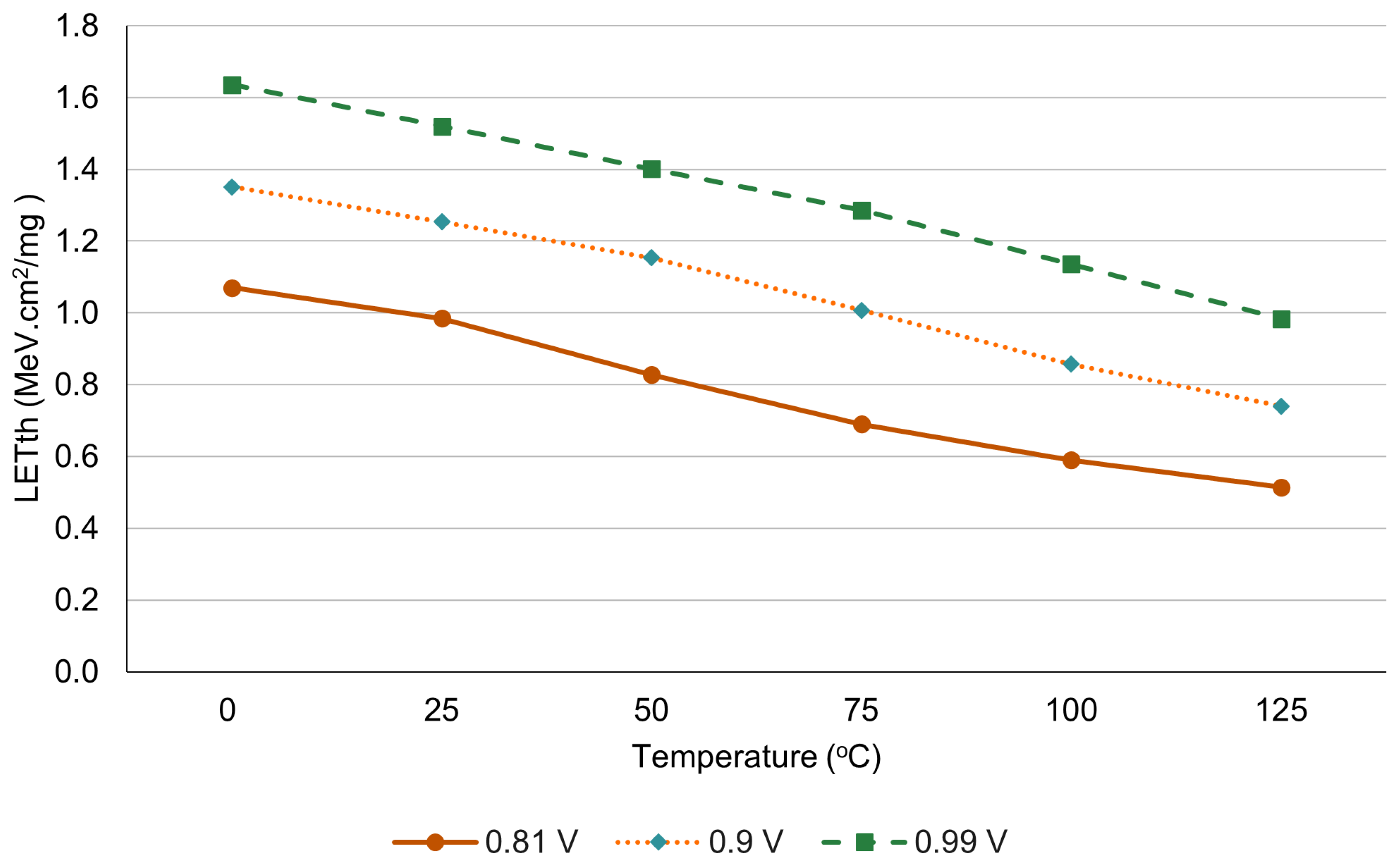
Finally, the impact on the LETth evaluation of temperature and voltage is described in
Figure 21, which shows the expected result that higher temperatures reduce cell robustness, as well as causing a voltage reduction. This behavior is similar to that reported by [
56] for XOR2 gates in other technology nodes.
5.3. Gate Mapping Case Study
During the circuit design, a crucial decision is how to map logical equations to a logical circuit. In this case study, we selected a classical benchmark: the ISCAS 85 C17 benchmark [
44] to explore three different gate mappings. Equation (
6) shows the logic equations for the C17. They are composed of two output functions. There are several ways to implement these equations as a circuit.
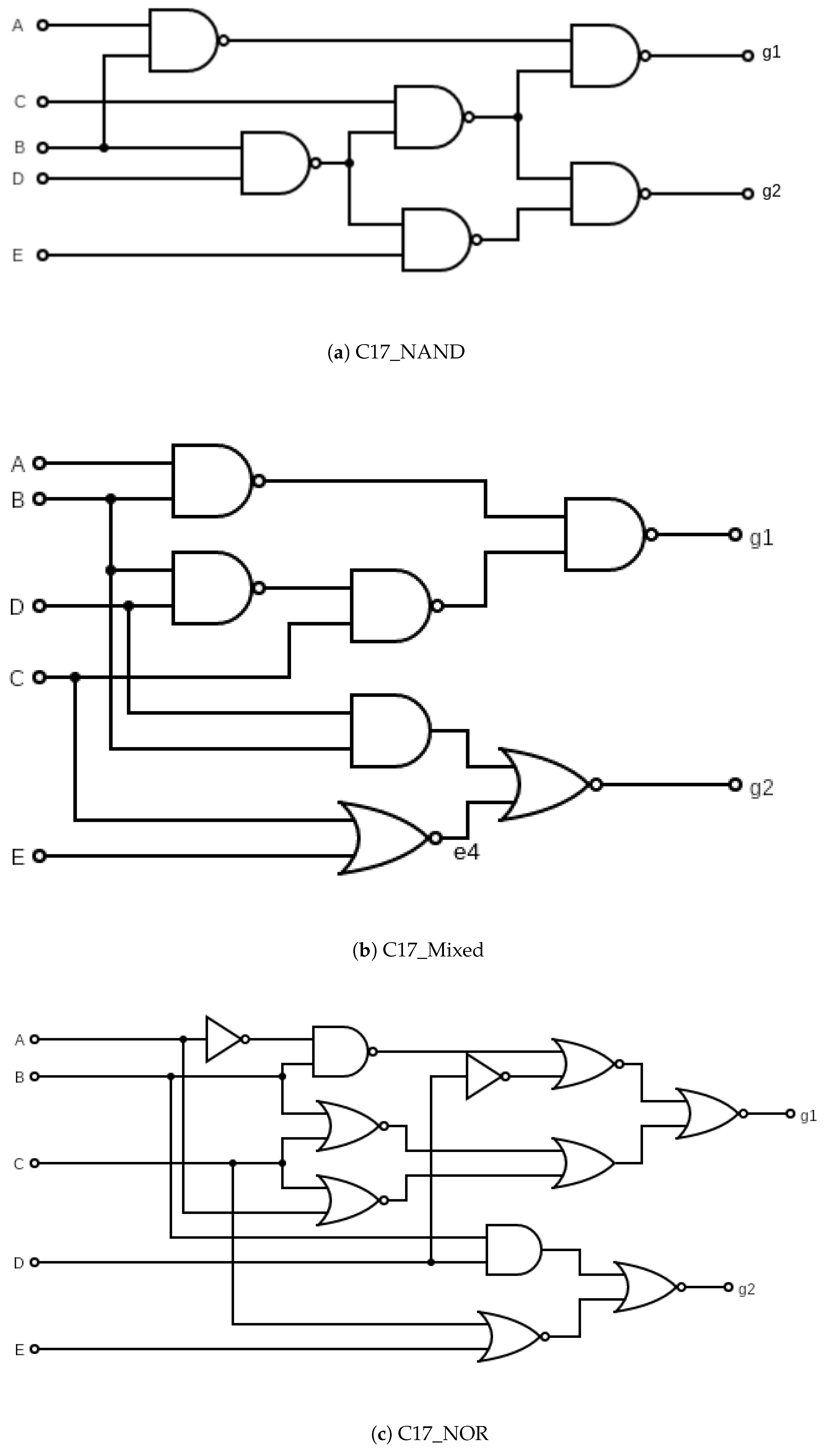
Figure 22 shows the three topologies for the C17 benchmark that were explored in this evaluation [
52]. Circuits are labeled according to the logic gate at their outputs.
Table 6 shows the main statistics for the three topologies regarding radiation sensitivity, observing the LET
th of the circuits without considering process variability in the nominal column, and the distribution of the results considering process variability by the mean (
), standard deviation (
), minimum (Min), and maximum (Max) values. This experiment adopts the 7 nm ASAP PDK model [
45] Considering the robustness, the C17 circuits are divided into two distinct groups. The ones with 70.7 MeVcm
2/mg as their LET
th and the ones with 51.8. This separation can be explained by electrical masking. Typically, the most sensitive fault configuration of a circuit involves an output of the circuit as its faulted node or a node close to the output. This is because the fault propagation from a node far from the output will attenuate the current pulse. As the LET
th only considers the most sensitive fault configuration, a circuit’s nominal robustness will typically be the same as the minimal robustness of its output gates, explaining the separation.
At nominal conditions, C17_NAND appears to be the superior topology in terms of radiation robustness. However, process variability introduces further nuance to the discussion. The previously discussed impact of process variability on the robustness of NAND2 and NOR2 gates affects the C17 topologies, indicating that under certain process variability conditions, the NOR2 can be the most robust, and C17_NOR will outperform C17_NAND. Furthermore, this also explains why C17_Mixed has the lowest average robustness. This is because in every WF configuration, it has the most sensitive gate of the two as one of its outputs.
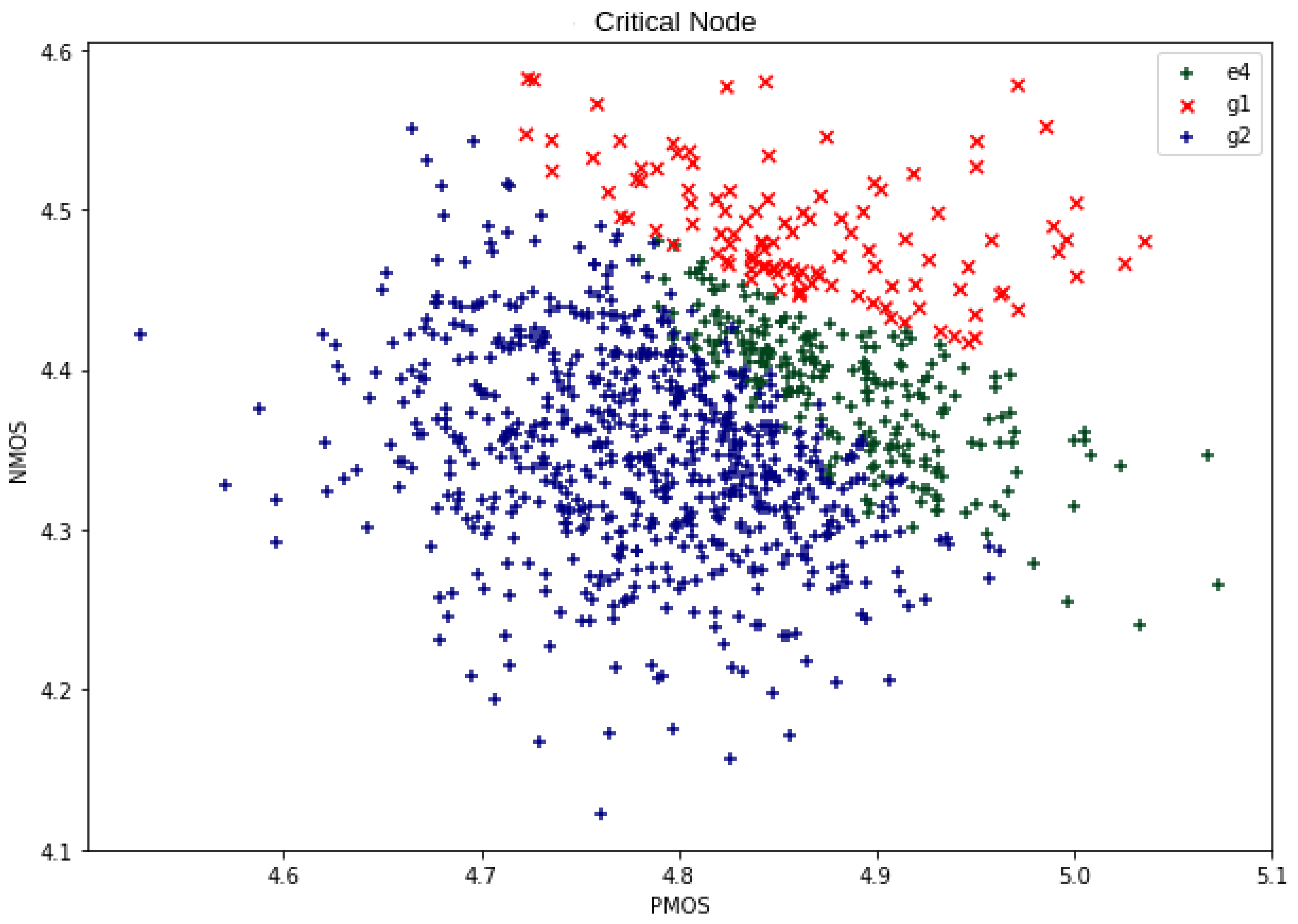
Figure 23 shows the most critical node of C17_Mixed at each point. The points marked with a cross indicate that the output
is the critical case; otherwise,
is the critical case. The proportion between the most sensitive output follows the same trend as the relation between the dominant gate shown in
Figure 16.
5.4. Comparison with Related Work
Finally, to assess Quasar’s correctness as a radiation reliability evaluation tool, the results generated by it were compared to similar results generated with other tools. For this purpose, the related work [
55] was chosen as it presents results related to critical charge, an equivalent metric to the one Quasar uses, and employs a different method of simulation and modeling to Quasar.
The evaluated circuit was NAND3 with a 32 nm bulk CMOS topology; this was compared with the findings reported in [
55] for the IHP 130 nm PDK [
57]. Both cases used the minimal sizing for every transistor. Currently, the transistor model used by [
55] is not supported in Quasar’s implementation, so we opted to conduct a comparison of related work using these two different technologies to observe the relative critical charge. Thus, it was still possible to compare the results by assessing how circuit state impacts robustness. However, the adoption of different technology nodes means that each transistor model had different results due to their different electrical properties. All input states were considered, and only faults originating on the output node were analyzed. The results are presented as critical charge instead of LET, as this is the metric used by [
55].
Table 7 shows the values found using both methodologies. The rows are ordered from the most robust state to the least robust. This is the first notable similarity: the order of robustness is the same in both cases. The grouping of fault configurations for the input vectors is also maintained; i.e., configurations of input vectors with only one input in the high state have similar critical charges in both cases, and the same is observed for input vectors with two high states. This grouping also occurred due to the restoring currents, where, for every n-hit case, every input in the low state represents a transistor to the source in conduction, which helps with charge restoration. More transistors during conduction accelerate the restoration, leading to higher critical charges. The p-hit case is a critical fault configuration due to the restoration being performed by the serial network.
Furthermore, for every case, the critical charge for the 32 nm transistor is lower than that of the 130 nm transistor, which is expected, as larger planar transistors usually require a higher charge to fault. The ratio between the two methodologies also has a low variance. This indicates that, despite being implemented in different technologies, the proportion of faults themselves is remarkably similar. Finally, this comparison not only demonstrates that Quasar can generate equivalent results to those of other technologies, but also shows that, even when different transistor implementations are used, the same circuit topology exhibits a known behavior.
6. Conclusions
This work details the development, features, and resources available in the Quasar tool, which accelerates and facilitates the easy evaluation of radiation effects on circuits at both the transistor and circuit levels, considering process variability effects. The current version of Quasar explores algorithm optimizations that reduce the number of electrical simulations required to search for the critical LET threshold, as well as the k-nearest neighbors regression approach, to further reduce the average number of simulations per fault configuration executed.
The proposed tool is useful for evaluating different types of circuits across various technology nodes and for portability, allowing it to run multiple electrical simulation tools simultaneously. The open code and modularity of the tool enable the easy integration of new resources, support for new technology nodes, and specific electrical simulation requirements. The scalability of the tool is under evaluation. The largest circuit currently evaluated is the C17 benchmark; however, we intend to extend the scalability evaluation to include larger circuits. At this moment, to the best of our knowledge, no software limitation restricts the evaluation of a large combinational circuit from the perspective of Quasar implementation, except for the electrical simulation runtime required. Also, the proposed tool could be expanded, with new modules being developed and included in the open access code to deal with some particular demand of the target CMOS circuits, or integrated in other physically modeled systems, to expand its application to domains where the Finite Element Model (FEM) could be used to simulate the physical environment surrounding the circuit, such as in biomedical or wearable systems. A recent work shows how the integration of FEM with AI-based monitoring enables robust signal processing under variable physical conditions in the real world, which often induces electrical disturbances [
58]. This approach could provide a multidisciplinary validation framework for Quasar, linking physical stress, deformation, or electromagnetic interference to circuit-level fault sensitivity.
