1. Introduction
Static Random-Access Memories (SRAMs) are widely used in modern electronic systems due to their high speed, low latency, and integration density. However, their sensitivity to radiation-induced Single-Event Upsets (SEUs) makes them critical components in environments such as aerospace, automotives, and high-performance computing [
1]. In practical applications, SRAMs are embedded in complex systems, where their reliability is essential. For instance, Chen et al. [
2] present a design of an SEU-tolerant 2D-FFT on SRAM-based FPGAs, highlighting the growing demand for radiation-hardened solutions in reconfigurable architectures. Similarly, De Caro et al. [
3] demonstrate the use of SRAMs in an all-digital spread spectrum clock generator for SoC synchronization, operating at GHz frequencies in 65nm CMOS, an environment where even low-energy particles can trigger bit upsets.
In such contexts, accurate SEU cross-section estimation becomes fundamental for system reliability. The proposed approach facilitates early-stage design optimization by enabling designers to evaluate the SEU vulnerability of different transistor sizing strategies, layout configurations, or technology choices, using only basic technological assumptions. This allows circuit architects to explore trade-offs between performance, area, and radiation robustness, and to implement mitigation techniques (e.g., transistor upsizing, cell redundancy, layout-level hardening) more effectively. In this sense, the methodology acts as a predictive analysis tool that bridges the gap between physical-level effects and circuit-level design decisions, without relying on proprietary process data or long simulation times.
While experimental irradiation is the standard for SEU characterization, it is often costly, time-consuming, and inaccessible during early design stages [
4]. Given these limitations, Technology Computer-Aided Design (TCAD) simulations offer a precise alternative at the device level [
4,
5,
6]. This involves solving Poisson’s equation, which determines the electrostatic potential distribution in the device, and the continuity equations, which compute the spatial and temporal distributions of carriers. Despite the precision offered by TCAD, these simulations are highly complex due to the number of input parameters, in-depth understanding of device structure, and underlying physics needed. TCAD simulations frequently require 3D modeling, which increases the complexity and computational time, making them impractical for large circuit analysis.
In contrast, at the circuit level, the Simulation Program with Integrated Circuit Emphasis (SPICE) offers a simpler and quicker simulation method. Although they lack the detailed physical modeling of TCAD simulations, SPICE are well-suited for evaluating the overall behavior of circuits. However, accurate prediction of radiation effects necessitates meticulous attention to material composition and particle–matter interactions [
7].
Consequently, SPICE simulations are frequently integrated with TCAD through a mixed-modeling technique. This hybrid approach streamlines the simulation process by modeling only the critical parts of the circuit using TCAD, while the remainder of the circuit is represented at a higher level of abstraction in SPICE. Both TCAD and SPICE modeling critically depend on the technology’s Process Design Kit (PDK) for accurate simulations. A PDK encompasses a detailed compilation of files, libraries, and models, encapsulating process parameters, electrical characteristics, and design rules specific to a manufacturing process. However, obtaining the PDK parameters by manufacturers is generally not straightforward [
8], leading to traditional simulations based on limited technological information, which may not achieve the desired accuracy.
In this context, this work proposes a methodology of estimating the SEU cross-section that deals with the disadvantages related to the simulation time, lack of technological information, and high complexity of the TCAD simulations. The standard 6T SRAM cell is the DUT for heavy-ion irradiation in 65 nm and 45 nm planar-bulk CMOS technology. The main objective of this approach is to provide a comprehensive method to estimate the SEU cross-section by using only the basic technological data available in the literature, or to discuss ways to estimate this data when unavailable. Furthermore, this work provides an in-depth analysis of the input parameters that most significantly affect TCAD modeling. The proposed methodology’s accuracy is validated by comparing simulation results with actual experimental data, ensuring a robust and practical alternative for SEU cross-section estimation.
2. Proposed Modeling
Although the SEU cross-section involves three-dimensional (3D) effects, two-dimensional (2D) modeling can be effectively used to simplify the simulation complexity and save calculation time. In this work, we apply mixed modeling using the version 2.28 of ECORCE TCAD tool [
9]. Other commercial TCAD tools can be used, but we chose ECORCE because it features an automatic and dynamic mesh generator that optimizes mesh distribution for all modeling steps, providing a high-quality grid, independent of the TCAD user. This feature was only available within ECORCE in 2015 [
9], and to our knowledge, this is still the case today. Also, ECORCE does not consider a constant Linear Energy Transfer (LET) over the ion track, but it uses the LET variation, including the Bragg peak, which provides a realistic representation of energy deposition. For the SPICE part, we used the open-access Predictive Technology Model (PTM) [
10]. The PTM bridges the process/material development and the circuit simulation through a compact device model, supporting early design analysis. This model was developed at Berkeley University using the BSIM4 as a basis [
10].
2.1. TCAD Modeling and Parameters
In mixed-modeling simulations for SRAMs, the NMOS transistor is typically selected over the PMOS transistor due to its higher vulnerability to SEU effects.
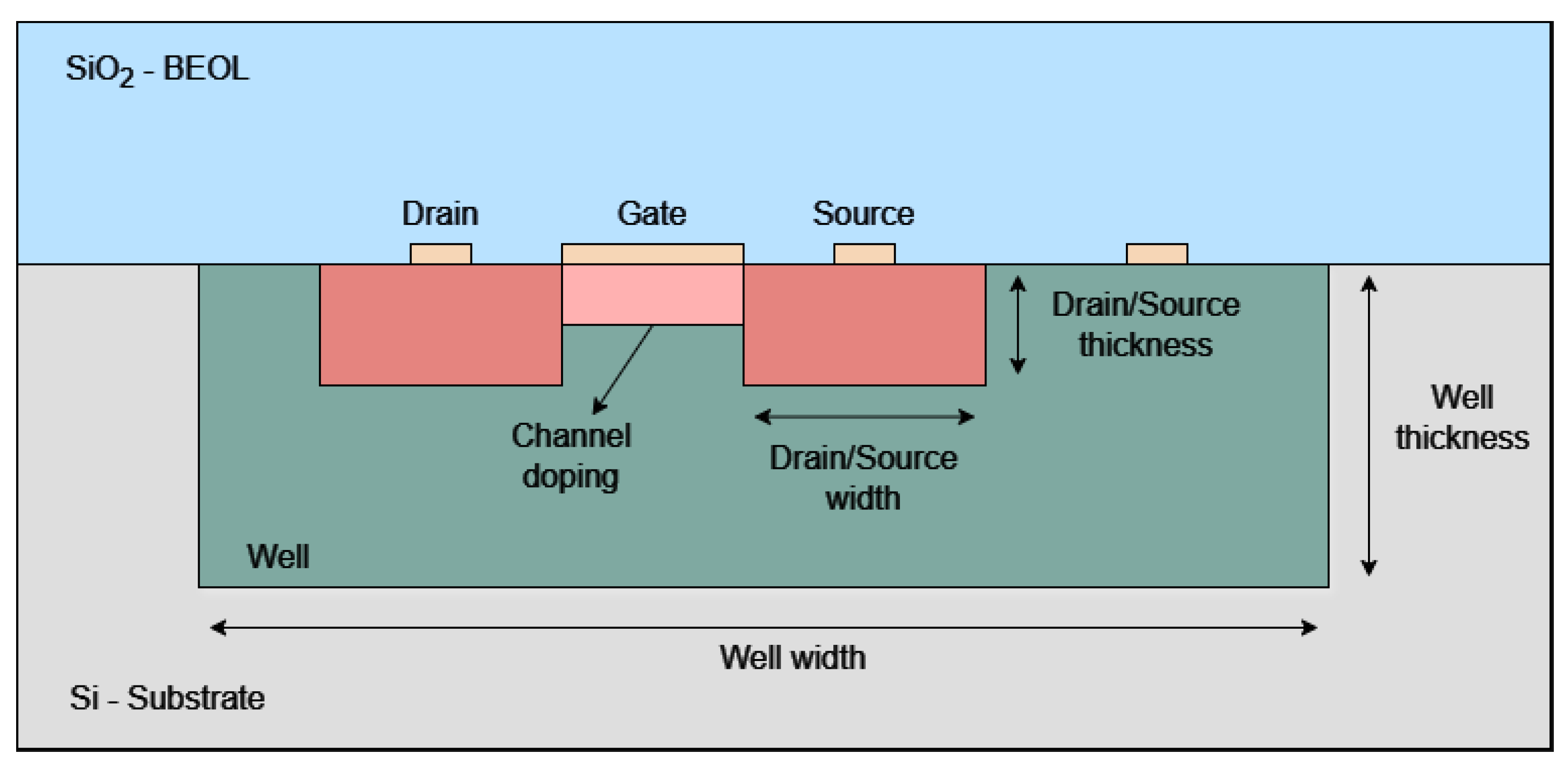
Figure 1 illustrates the simplified NMOS transistor structure implemented in ECORCE.
Table 1 presents the parameters, and their corresponding values are utilized in the simulations.
For planar-bulk CMOS technology, the channel width is generally guided by the transistor technology node. However, this estimation may vary due to differences in manufacturer specifications and design priorities, such as optimization for high performance or low power applications. In this work, we adopt channel width values in accordance with the PTM. Similarly, parameters such as oxide thickness, drain/source doping, and well doping are also sourced from the PTM. The drain/source width is generally ~2.5 times the channel length [
11]. This configuration ensures a general representation of the NMOS device structure for SEU cross-section estimation. Given the typically undisclosed composition of the Back-End-Of-Line (BEOL) layer, the modeling proposed here assumes an 8 μm thick silicon dioxide (SiO
2) layer. Although this approximation is not perfect, it serves as a practical solution for simulating the energy loss of impinging particles. The substrate is modeled using a 20 μm thick bulk silicon (Si) layer. Additionally, the transistor structure includes a 1 μm border width on both sides, which is essential for calculating the SEU cross-section based on the particle impact position. A narrower border could affect the SEU cross-section calculation by potentially overlooking faults occurring near the device’s edges, while increasing the border width would require a higher number of particle injections. This would increase the accuracy, but also the simulation time. After testing border widths ranging from 0.5 μm to 3 μm, we found that 1 μm provided a good trade-off for this analysis. The substrate doping is estimated at 6 × 10
16 cm
3, which optimizes transistor performance.
Conversely, the specification of certain parameters, such as the thicknesses of the doping regions and the channel doping value, poses a more intricate problem. In this study, we chose a set of parameters that provide a transistor characteristic consistent with SPICE simulations. The used values are included in
Table 1, while the details regarding them are further explained in
Section 4.
Both NMOS transistors were simulated on ECORCE with a mesh precision of 3 nm, utilizing approximately 4500 mesh nodes for 65 nm and 3000 nodes for 45 nm. The electrical characterization takes around 8 min, using 4 cores of a standard commercial processor.
Figure 2 illustrates the drain current (I
drain) versus the gate voltage (V
gate) for the transistors in 65 nm and 45 nm technology, comparing the ECORCE transistor with the SPICE one. The V
drain is 1.2 V for the 65 nm and 1.0 for the 45 nm, following the expected node voltage of the SRAM cell. The leakage current, threshold voltage, and saturation current exhibit close correspondence, showing a good calibration between the transistors. However, there are some discrepancies in the curve shape, which can be attributed to different physical laws accounted in the TCAD simulation with respect to the simplified ones of the SPICE predictive model. ECORCE relies on a drift–diffusion TCAD framework that numerically solves Poisson’s equation and the continuity equations for electrons and holes, while accounting for detailed physical mechanisms such as doping-dependent mobility, carrier recombination, velocity saturation, and impact ionization. In contrast, the SPICE model used in this study is based on the BSIM4 compact model from the Predictive Technology Model (PTM), which uses empirical equations calibrated to measured data, and does not resolve spatial charge transport in the same manner.
Additionally, it is important to note that some of the device parameters used in the TCAD model were estimated based on the literature and SPICE model assumptions, given the lack of access to full PDK data. These estimations, especially for doping profiles, can also influence the electrical behavior of the simulated transistor and contribute to the observed differences between the models. Despite these limitations, the calibration remains sufficiently accurate for the purposes of SEU analysis within the proposed methodology.
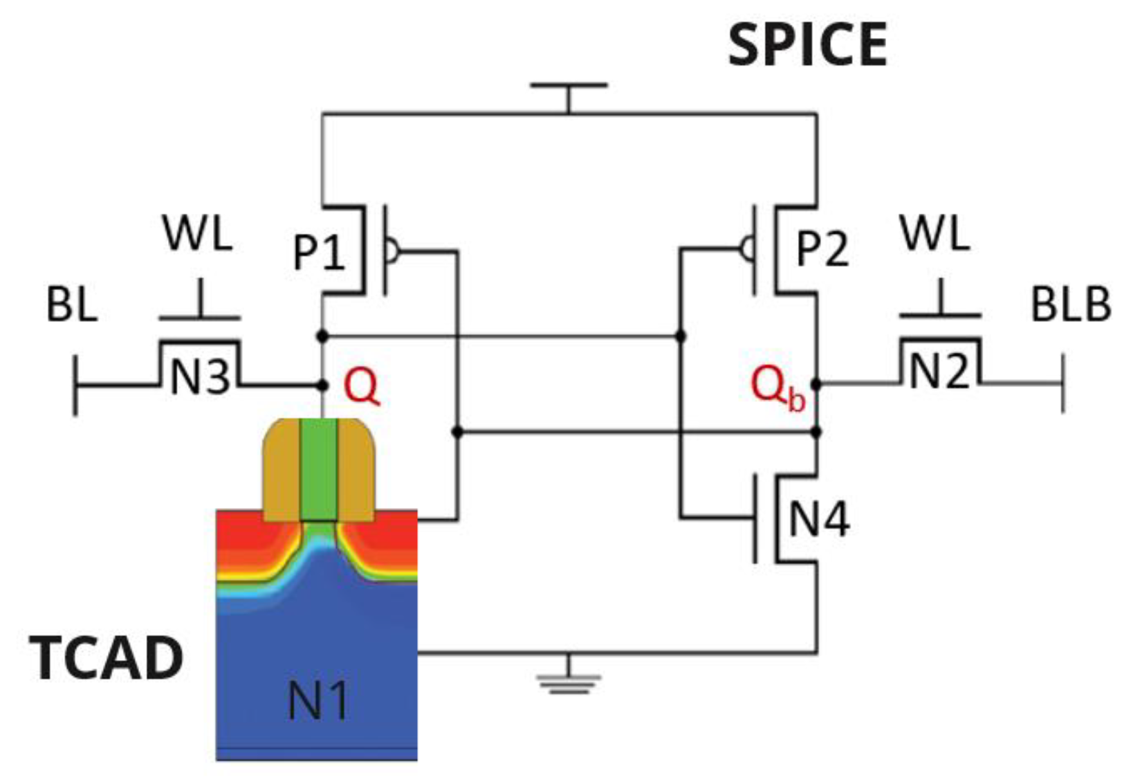
2.2. SPICE Circuit Implementation
The SPICE model will be used to simulate the remaining five transistors of the 6T cells.
Figure 3 illustrates the 6T SRAM cell circuit in detail. For this, it is necessary to define each transistor’s width (
W) to length (
L) ratio. The proper sizing of transistors in the cell is crucial for ensuring reliable read and write operations. To optimize the read operation, the cell ratio (
CR) is expressed as
CR =
(WN1/LN1)/(WN3/LN3) or
(WN4/LN4)/(WN2/LN2), while for the write operation, the pull-up ratio (
PR) is defined as
PR =
(WP1/LP1)/(WN3/LN3) or
(WP2/LP2)/(WN2/LN2) [
12]. In this work, the design choices include a CR = 1.5 and a PR = 1.0. The minimum W/L used for each technology follows an approximate ratio of 2, representing a standard choice that balances cell area and delay time, while providing good static and dynamic noise margins [
13]. However, it is essential to note that other values can be used, depending on specific project requirements.
2.3. SEU Cross-Section Calculation
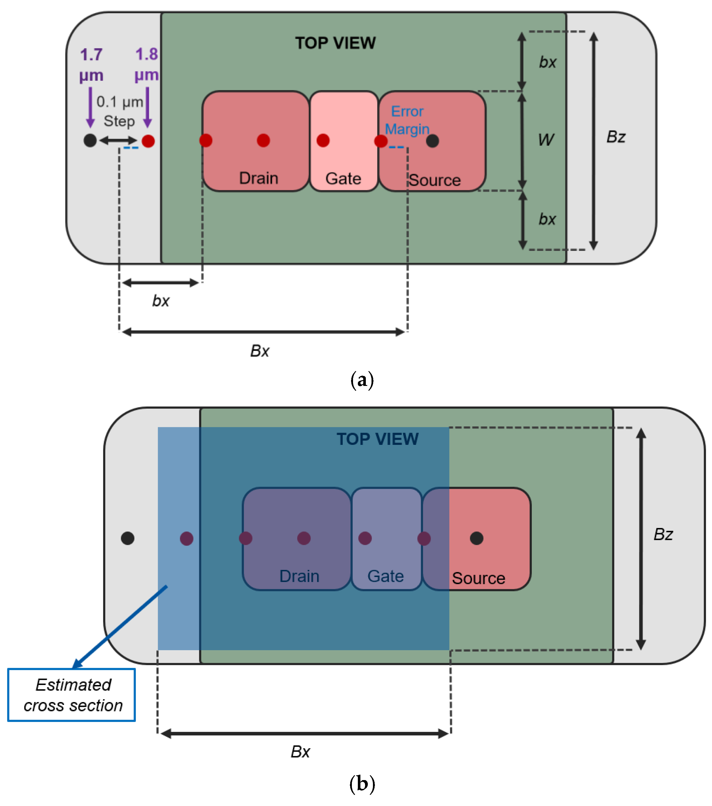
In recent years, numerous simulation approaches have been proposed to evaluate the SEU cross-section. Most of these approaches offer very accurate results but require a large computational cost. In this proposed methodology, the emphasis is on a simplified approach with targeted ion injections along the
x-axis, maintaining a precise 0.1 μm spacing between each injection. Given the dimensions of a 65 nm transistor, for example, this strategy necessitates only 29 injections per ion in order to investigate its effects on the transistor. This analysis encompasses an evaluation of six different ions, drawing data from the RADiation Effects Facility (RADEF) heavy ions 16.3 MeV/u database to ensure a broad spectrum is covered.
Figure 4 shows the method used to calculate the SEU cross-section.
In the first step, for each injection we check the SEU occurrence (red points in
Figure 4a). With this, we can calculate the sensitivity along the
x-axis, denoted as
Bx. It is important to note that, since we chose a 0.1 μm step between each injection, there is some uncertainty in this range. To take this into account, a margin of error of ±0.05 μm (half of the step) was added. Next, we calculate the sensitive region up to the drain, referred to as
bx. By adding the transistor width (
W = 0.18 μm for the 65 nm node and
W = 0.09 μm for the 45 nm node) with twice the value of
bx, we obtain the sensitive region along the
z-axis, denoted as
Bz. Equation (1) shows this calculation. Multiplying
Bx by
Bz yields the SEU cross-section for the NMOS transistor.
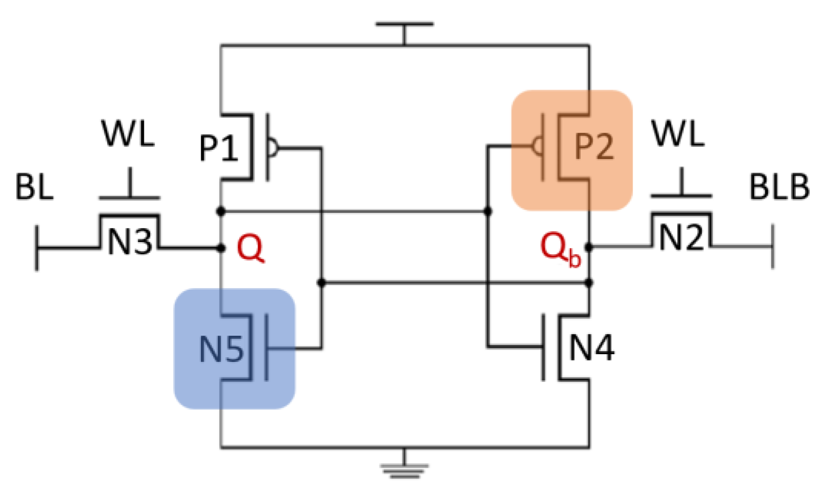
In an SRAM cell, bit storage relies on a pair of inverters in a feedback loop configuration, meaning that one NMOS transistor and one PMOS transistor are always in the OFF-state simultaneously (i.e., both are sensitive at same time).
Figure 5 illustrates this behavior in the SRAM circuit. In this sense, the cross-section of the cell can be expressed by Equation (2):
To incorporate the effect of the PMOS transistor without requiring an additional simulation, we propose to take into account the sizing ratio between the NMOS and PMOS transistors. With a chosen CR = 1.5 and PR = 1.0, the NMOS transistor is 1.5 times larger than the PMOS. Finally, dividing the calculated NMOS cross-section by 1.5 and adding this value to the NMOS cross-section, we can obtain an estimation of the cell cross-section. Equation (3) presents this calculation.
This approximation is proposed to accelerate the analysis by avoiding additional TCAD simulations for the complementary PMOS transistor. However, the methodology remains flexible, and users can model the PMOS separately if higher precision is required.
3. Experimental Validation
In this section, the estimation of the 6T SRAM SEU cross-section under heavy-ion irradiation is compared with experimental data obtained from the literature [
14,
15]. Based on the simulation results, a Weibull curve is generated to fit the calculated points. The error margin is 1 × 10
−10 cm
2/bit.
For the 65 nm SRAM, the results are shown in
Figure 6, which shows a good agreement between simulation and experimental data for medium-high LET values. However, in the threshold LET (LET
th) region, the results present a divergence in comparison with the experimental data. We did not observe upsets in 1.3 MeV·cm
2/mg, and our result for 2.3 MeV·cm
2/mg exhibits an underestimation. This behavior is linked to our simplifications, the assumed SiO
2 thickness in the BEOL layer, the doping value of the well, and the substrate doping. When ions pass through the BEOL, they lose energy, affecting carrier generation. At low LET, the ion generates a voltage peak very close to the threshold voltage of the transistor, and small variations in the carrier generation can affect the cross-section calculation. Another crucial point to note is the high error bar for 2.3 MeV·cm
2/mg, which happens due to the 0.1 μm step used in ion injection.
The 45 nm SEU cross-section estimation presents an even better agreement between simulation and experimental data. The results are shown in
Figure 7. Both LET
th and saturation regions are in good agreement. The predictive SPICE model seems more accurate for this technology node. Consequently, the parameter approximation has greater impact on the simulation behavior. This demonstrates the viability of the proposed methodology, especially when the parameters extracted from the spice model are similar to that of the device tested.
The proposed methodology proved to be an excellent option for predicting the SEU cross-section at medium-high LET values for supply voltage. The simulation accuracy drops slightly in the LET
th region for 65 nm node. However, these results are impressively accurate when considering the number of simplifications made at the circuit and device level. At this point, no input parameter fitting is performed to reach a better SEU cross-section result. Another key point is the reduced simulation time. Normally, simulating the impact of a single ion on a SRAM cell may take days, depending on the TCAD implementation [
16], whereas our approach yields complete results across a range of LET values in approximately 15 h.
5. Conclusions
The proposed methodology for estimating SEU cross-sections shows a strong correlation with experimental irradiation data, despite some deviations in specific regions. Importantly, these results were obtained without relying on proprietary PDK data or complex TCAD configurations, using only academic and predictive models. The simulation results for 65 nm and 45 nm SRAMs under heavy-ion irradiation demonstrate the effectiveness of the method across a wide range of LET values. The 45 nm case exhibited excellent agreement with the measured data, while the 65 nm case showed good correlation in the mid-to-high LET range. The discrepancies observed at lower LET values for 65 nm are attributed to the fixed injection step size, simplifications in the SPICE model, and assumptions made for doping profiles.
Overall, this methodology enables the efficient and practical evaluation of SEU cross-sections even in scenarios where detailed technological data is not available. It also lowers the entry barrier for engineers and researchers without extensive TCAD experience, offering a straightforward path to radiation effect analysis.
Compared to traditional approaches, which may require several days per injection, our approach produced complete SEU cross-section curves in approximately 15 h. These results confirm that the proposed method is both effective and computationally efficient, offering a valuable alternative for early-stage design analysis and SEU sensitivity estimation under heavy-ion irradiation.
Although the methodology has proven effective for planar bulk CMOS technologies, it currently remains constrained to SRAM cells with symmetric layouts, where the sensitive area between transistors can be reasonably estimated using the cell ratio. Extending the methodology to more complex or asymmetric circuits is technically feasible but would significantly increase simulation time due to the need to model multiple individual transistors in TCAD. Furthermore, the method has not yet been validated for more advanced technologies such as Fully Depleted Silicon On Insulator (FDSOI) and Fin Field-Effect Transistor (Fin-FET) structures, which exhibit different charge collection dynamics and may require 3D TCAD modeling for accurate SEU estimation.


 ,
, 


