Article

Total Ionizing Dose Effects on Lifetime of NMOSFETs Due to Hot Carrier-Induced Stress

1
School of Microelectronics, Xidian University, Xi’an 710071, China
2
Science and Technology on Reliability Physics and Application of Electronic Component Laboratory, China Electronic Product Reliability and Environmental Testing Research Institute, Guangzhou 511370, China
3
School of Optoelectronics and Communication Engineering, Xiamen University of Technology, Xiamen 361005, China
*
Author to whom correspondence should be addressed.
Electronics 2025, 14(13), 2563; https://doi.org/10.3390/electronics14132563
Submission received: 8 May 2025 / Revised: 19 June 2025 / Accepted: 24 June 2025 / Published: 25 June 2025

Abstract

This study systematically investigates the mechanism by which total ionizing dose (TID) affects the lifetime degradation of NMOS devices induced by hot-carrier injection (HCI). Experiments involved Cobalt-60 (Co-60) gamma-ray irradiation to a cumulative dose of 500 krad (Si), followed by 168 h annealing at 100 °C to simulate long-term stability. However, under HCI stress conditions (VD = 2.7 V, VG = 1.8 V), irradiated devices show a 6.93% increase in threshold voltage shift (ΔVth) compared to non-irradiated counterparts. According to the IEC 62416 standard, the lifetime degradation of irradiated devices induced by HCI stress is only 65% of that of non-irradiated devices. Conversely, when the saturation drain current (IDsat) degrades by 10%, the lifetime doubles compared to non-irradiated counterparts. Mechanistic analysis demonstrates that partial neutralization of E’ center positive charges at the gate oxide interface by hot electrons weakens the electric field shielding effect, accelerating ΔVth drift, while interface trap charges contribute minimally to degradation due to annealing-induced self-healing. The saturation drain current shift degradation primarily correlates with electron mobility variations. This work elucidates the multi-physics mechanisms through which TID impacts device reliability and provides critical insights for radiation-hardened design optimization.

1. Introduction

The rapid advancement of space science and aerospace technology has transformed deep space exploration from science fiction into an operational reality, with sustained Mars missions now exceeding 1500 sols and lunar base construction underway. While public attention often focuses on spectacular achievements like extraterrestrial landings, the engineering community faces critical reliability challenges in semiconductor devices that power these ambitious missions. Space radiation environments induce total ionizing dose effects that generate oxide trap charges and interface trap charges in MOS devices, causing threshold voltage drift and leakage current increases exceeding several orders of magnitude [1,2]. Concurrently, prolonged operational stresses during active mission phases subject devices to hot-carrier injection mechanisms, where electric fields > 6 MV/cm accelerate charge carriers, creating additional interface traps that degrade transconductance by 18–22% [3,4,5]. These parallel degradation pathways demonstrate striking similarities in their physical manifestations, yet current reliability assessments persist in evaluating them through isolated single-mechanism approaches.
Emerging evidence suggests synergistic interactions between radiation-induced defects and electrothermal stress mechanisms [6,7]. Accelerated aging tests reveal non-linear degradation patterns where combined TID-HCI exposure causes 40% greater threshold voltage shifts than linear superposition predictions, particularly in advanced 14 nm FinFET nodes. This interaction stems from radiation-created defect precursors lowering activation energy for subsequent hot-carrier damage by 0.15 eV, while trapped charges modify local electric fields to enhance carrier injection probabilities sixfold. Such cross-mechanism amplification effects remain unaddressed in current space qualification standards, potentially leading to 55–70% lifetime overestimations for five-year Mars missions.
Some combined studies on space radiation and electrical stress reliability in semiconductor devices have emerged globally [8,9,10,11,12,13,14,15]. References [8,9] conduct preliminary investigations on the combined damage of total ionizing dose radiation and hot-carrier injection in MOS capacitors, concluding that their synergistic damage effect does not follow simple linear superposition, though the underlying causes and mechanisms are not analyzed. Studies [10,11] have investigated the impact of different TID testing methodologies—such as direct HCI testing post-TID irradiation, or TID irradiation followed by high-temperature annealing and subsequent HCI testing—on the interplay between TID effects and HCI-induced degradation. Reference [12] examines TID radiation effects on hot-carrier behavior in 10 nm FinFET devices. Study [13] proposes TID-induced annealing effects in the buried oxide layer of SOI devices under HCI-induced stress, and Reference [14] reveals differential impacts of TID-induced charges on hot-carrier effects in n-channel versus p-channel FinFETs. Additionally, Reference [15] identifies layout-dependent radiation-enhanced hot-carrier degradation in 65 nm MOS devices. However, these studies rarely analyze the impact of the combined stress of total ionizing dose irradiation and hot carriers on device degradation lifetime.
This study investigates the impact of TID irradiation on the hot-carrier lifetime of NMOS devices. Co-60 radiation is employed to irradiate the devices with a total dose of 500 krad (Si), followed by annealing at 100 °C for 168 h. HCI stress tests under three voltage conditions for 5000 s are conducted on both irradiated and non-irradiated devices to analyze their characteristic degradation and defect evolution under combined TID and HCI stress. According to the IEC 62416 standard for device lifetime calculation under hot-carrier injection effects, the lifetime under HCI stress associated with a 10% increase in threshold voltage for irradiated devices is approximately 65% of that for non-irradiated devices. Conversely, when the saturation leakage current decreases by 10% under HCI stress, the lifetime of irradiated devices is approximately twice that of non-irradiated devices.

2. Materials and Methods

The tested devices are Bulk N-Metal-Oxide-Semiconductor (NMOS) transistors fabricated by the Semiconductor Manufacturing International Corporation (SMIC), featuring a gate oxide thickness of 2 nm, a gate length of 130 nm, and a width-to-length ratio (W/L) of 100:1.
The total dose irradiation test is conducted with a dose rate of 50 rad (Si)/s and a total radiation dose of 500 krad (Si), under ON bias conditions (gate voltage VG = 1.2 V, drain voltage, source voltage, and substrate voltage VD = VS = Vsub= 0 V). Irradiation is performed at the Xinjiang Technical Institute of Physics and Chemistry, Chinese Academy of Sciences with a Cobalt-60 source. Following the total dose irradiation, an annealing test is conducted at a high temperature (100 °C) under ON bias for a duration of 168 h. Given that the actual space environment exhibits an extremely low dose rate (0.01 rad (Si)/s), high-temperature annealing tests following total ionizing dose irradiation are adopted to simulate space radiation effects. This approach ensures that the combined TID and HCI stress testing results more accurately reflect realistic space operating conditions.
According to the IEC 62416-2010 standard [16], the drain voltage for hot-carrier testing is determined based on the device’s drain breakdown voltage. The gate voltage is specified by applying the maximum substrate current method at each corresponding drain bias. Both the source and the substrate are connected to the ground. The test conditions for the hot-carrier test are presented in Table 1, and the test is performed under room temperature conditions (25 °C ± 2 °C).
The hot-carrier test conditions for samples subjected to total dose rate irradiation, post-irradiation annealing, and non-irradiated samples are identical. For each sample under each test condition, five devices are subjected to the hot-carrier test, with a test duration of 5000 s. The I-V characteristics of the NMOS devices are measured using the Keysight 1500 A Semiconductor Device Parameter Analyzer (Keysight Technologies, Santa Rosa, CA, USA). The Keysight 1500 A offers voltage measurement accuracy at the 1 μV level and current measurement accuracy at the 1fA level.

3. Results and Discussion

3.1. Irradiation and Annealing Test Results

The transfer characteristic curves (ID-VG curves) before and after total dose irradiation and annealing tests are shown in Figure 1.
Experimental results demonstrated distinct radiation effects and recovery behaviors in NMOS devices: Under a total ionizing dose of 500 krad (Si), the threshold voltage exhibited exceptional stability with a drift of <5 mV, confirming minimal oxide charge trapping influence on gate control. However, off-state leakage current surged from 10−9 A to 10−7 A due to radiation-induced interface traps creating parasitic conduction paths. Subsequent annealing at 100 °C for 168 h fully restored leakage to 10−9 A and recovered the ID-VG curve to its pre-irradiation profile, attributed to hydrogen-mediated passivation of interface defects during thermal treatment. These findings establish that while ionizing radiation primarily degrades off-state leakage through trap-assisted tunneling, standard annealing protocols can completely reverse such damage without compromising threshold voltage integrity, highlighting the robustness of NMOS devices in radiation-aware applications.
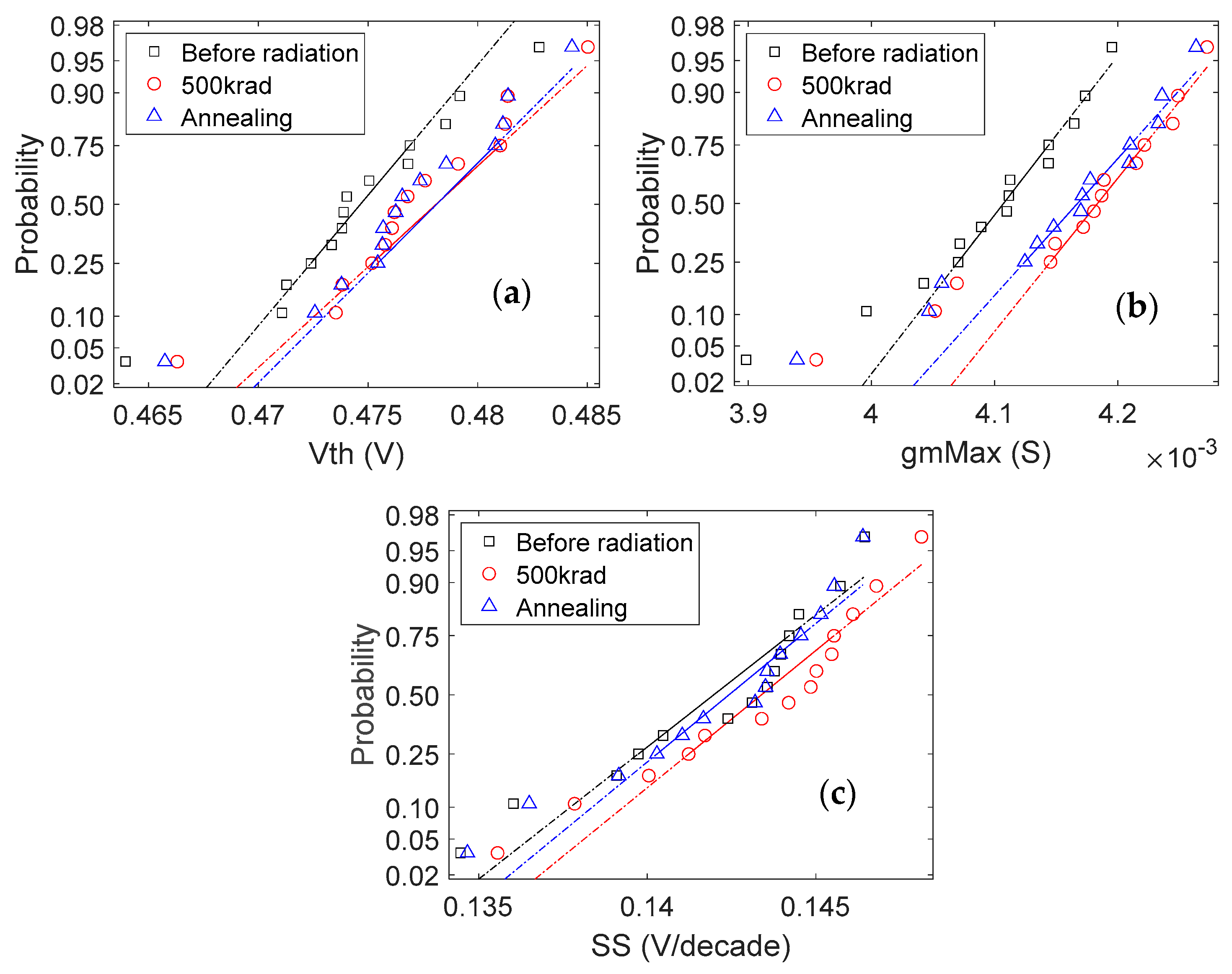
To spread device-to-device variation effects on irradiation and annealing responses, threshold voltage, maximum transconductance (Gm-max), and subthreshold swing (SS) distributions are statistically analyzed across multiple devices, as shown in Figure 2. Notably, the ID range of 10−5 A to 10−4 A is selectively used for SS extraction to eliminate miscalculations caused by radiation-elevated off-state leakage currents. The threshold voltage shifted from 0.4745 V (pre-irradiation) to 0.4771 V after 500 krad irradiation, only resulting in a ΔVth of +2.6 mV. This positive drift dominance indicates that interface trap charges (contributing to Vth increase) outweighed oxide-trapped charges (inducing Vth decrease). Post-annealing Vth remained at 0.4768 V, showing no significant recovery trend. Further analysis of SS demonstrated irradiation-induced degradation from 0.1420 V/decade to 0.1433 V/decade, consistent with interface trap generation, followed by near-complete restoration to 0.1421 V/decade after annealing. The change in the maximum transconductance value is also very small during the total dose irradiation process, and the change in the maximum transconductance value after irradiation is less than 1 mS.
The persistent Vth stability during annealing suggests a balanced recovery mechanism: both oxide-trapped charges and interface traps recovered at comparable rates, with their opposing contributions (negative vs. positive Vth drift) resulting in a net-zero drift. These observations confirm that while interface traps dominate SS degradation and partial Vth shifts, the counteracting recovery dynamics between oxide and interface charges maintain Vth homeostasis during thermal treatment.

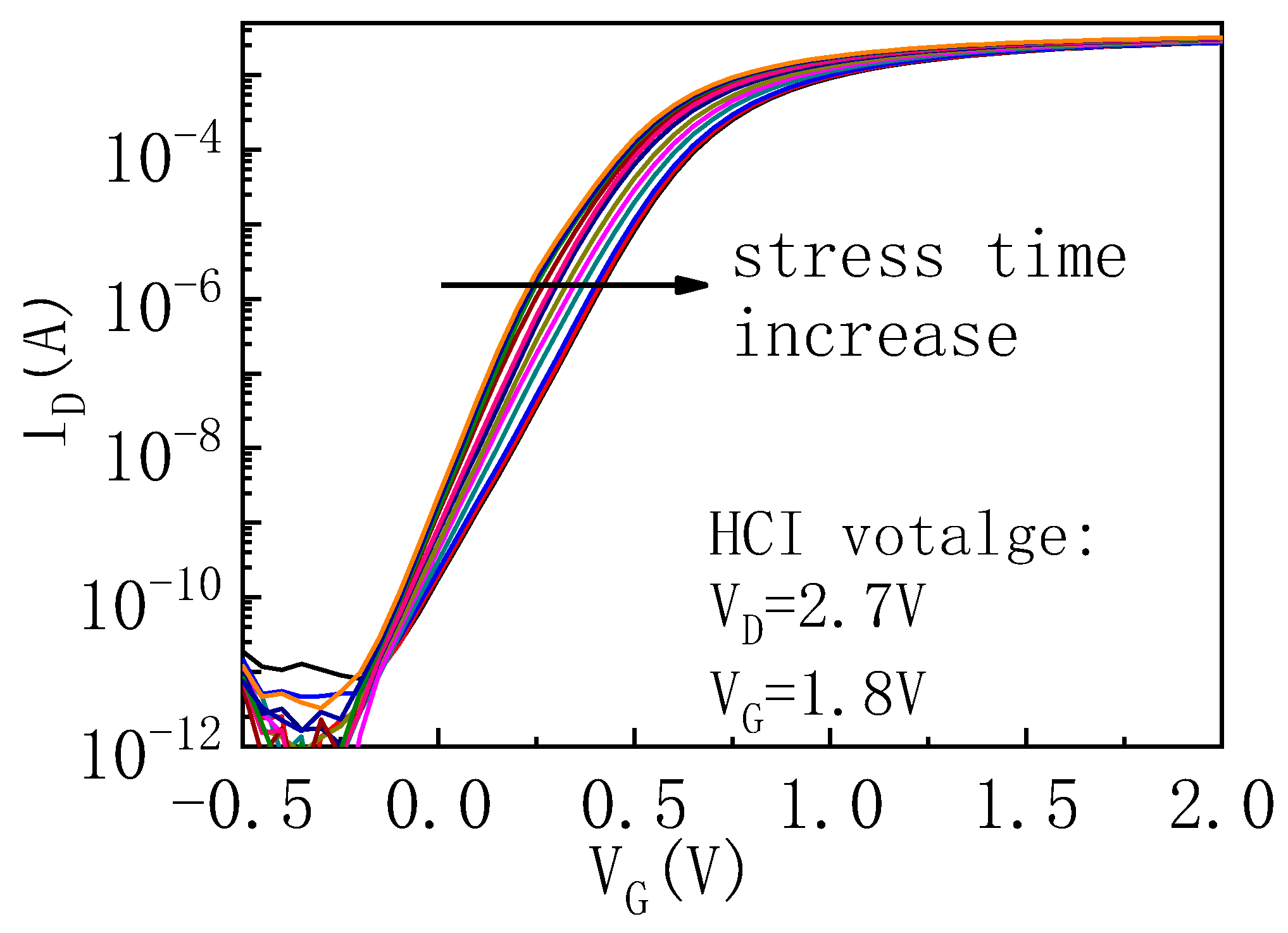
3.2. Hot-Carrier Test Results

After conducting irradiation and annealing tests, hot-carrier tests are performed. The ID-VG curves under different time conditions are shown in Figure 3. The results reveal that during the hot-carrier test, the threshold voltage exhibited a positive shift, and the slope of the subthreshold region decreased, indicating an increase in the subthreshold swing.
The Vth variations during irradiation, annealing, and hot-carrier tests are illustrated in Figure 4. The results show that the Vth of the NMOS device is insensitive to TID irradiation, with minimal changes induced by irradiation (ΔVth ≈ 2.6 mV, as shown in Figure 2a). However, during the hot-carrier test, the threshold voltage increased rapidly. At HCI condition 1, the Vth rose from 0.4771 V to 0.6598 V after 10,000 s of hot-carrier stress, resulting in a ΔVth = 182.7 mV. This shift is significantly higher than the average ΔVth caused by TID irradiation (2.6 mV), highlighting the severe degradation under hot-carrier stress compared to irradiation effects.
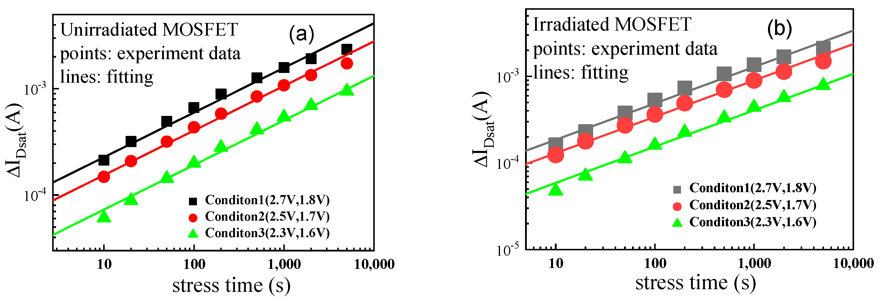
Hot-carrier injection tests are performed on both non-irradiated and irradiated devices under identical conditions. Figure 5 illustrates the average values and variances of threshold voltage shift (ΔVth) and saturation drain current shift (ΔIDsat) for five devices under three stress conditions as functions of testing time under hot-carrier stress. ΔVth represents the change in threshold voltage between before and after HCI testing, while ΔIDsat denotes the change in saturation drain current between before and after HCI testing. Observations from Figure 5 reveal that the degradation rate of ΔVth in total-dose-irradiated NMOS devices under HCI stress is slightly faster than that of non-irradiated devices, whereas the degradation rates of ΔIDsat under HCI stress are slower in irradiated devices compared to non-irradiated ones, exhibiting trends opposite to ΔVth. As shown in Figure 5a, under HCI Stress Condition 1 (VD = 2.7 V, VG = 1.8 V), the ΔVth of irradiated devices increases by 185 mV after 5000 s of HCI stress, while non-irradiated devices show a ΔVth of 173 mV, with a minimal difference of 12 mV. Under HCI Stress Condition 3 (VD = 2.3 V, VG = 1.6 V), the ΔVth values after 5000 s of stress are 71 mV (irradiated) and 68 mV (non-irradiated), differing by only 3 mV. This indicates that the ΔVth difference between irradiated and non-irradiated devices is negligible under low HCI stress but becomes more pronounced as stress intensity increases. In contrast, ΔIDsat exhibits an opposing trend to ΔVth. From Figure 5b, under HCI Stress Condition 1, ΔIDsat reaches −2.11 mA (irradiated) and −2.34 mA (non-irradiated) after 5000 s of stress, with a difference of +0.23 mA. Under HCI Stress Condition 3, ΔIDsat values are −0.79 mA (irradiated) and −0.95 mA (non-irradiated), differing by +0.16 mA. It is evident from Figure 5b that the saturation leakage current decreases with increasing HCI stress time. However, the reduction in saturation leakage current for the unirradiated device is less pronounced compared to the irradiated device, which is contrary to the variation trend of ΔVth. Furthermore, the difference in ΔIDsat between the irradiated and unirradiated devices increases slightly as the hot-carrier stress voltage rises.

3.3. Comparative Analysis of Hot-Carrier Lifetime

To quantitatively evaluate the impact of irradiation on hot-carrier degradation, degradation model parameters extracted before and after irradiation are compared.
According to IEC 62416-2010, the relationship between the degradation amount of MOS device parameters and the degradation time, as well as the stress voltage value, during hot-carrier injection effect testing can be expressed by the following formula:
Δ D = A × exp B / V d , stress × t C
where ∆D represents the degradation amount of the MOS device parameter caused by hot-carrier injection stress, A and B are coefficients determined through the same global fitting procedure, C is the degradation time exponent, and t is time. Based on Formula (1), the threshold voltage shift caused by hot carriers can be expressed by the following equation:
Δ V th = A × exp B / V d , stress × t C
Using the least squares method, a global fitting is performed based on Equation (1) for the degradation data for unirradiated devices under three stress voltages (VD,stress = 2.7 V, 2.5 V, 2.3 V), yielding the degradation time exponent C = 0.42 in Equation (2), as shown in Figure 6a.
By setting the stress time t = 100 s, the threshold voltage shift ΔVth at 1 s corresponds to the value of A × exp (B/VD,stress). Based on the linear relationship ΔVth @100 s~1/VD,stress, the coefficients are determined as A = 8.003 and B = −19.21. The hot-carrier degradation model for non-irradiated devices is expressed as follows:
Δ V th = 8.003 × exp 19.21 / V D , stress × t 0.42
Using the same model parameter extraction methodology, the hot-carrier degradation model for irradiated devices is derived as follows, with the parameter extraction process illustrated in Figure 6b:
Δ V th = 9.455 × exp 19.20 / V D , stress × t 0.42
According to the IEC 62416-2010 standard [16], based on the model Equations (3) and (4), using ΔVth = 50 mV (approximately 10% degradation of the initial Vth) as the failure criterion, the calculated hot-carrier lifetimes for non-irradiated and irradiated devices operating at VD = 1.2 V are 2.018 × 10¹¹ s and 1.330 × 10¹¹ s, respectively. This indicates that the hot-carrier lifetime for 10% threshold voltage degradation in irradiated devices is approximately 65% of that in non-irradiated devices, demonstrating that total ionizing dose radiation effects accelerate the degradation of threshold voltage under hot-carrier stress.
The saturation drain current variation ΔIDsat can be expressed by the following equation:
Δ I D sat = A × exp B / V d , stress × t C
By fitting the average ΔIDsat values of irradiated and non-irradiated devices (as shown in Figure 7), the hot-carrier degradation model for ΔIDsat in non-irradiated devices is derived as follows:
Δ I D sat = 0.0655 × exp 17.776 / V d , stress × t 0.42
Using the same parameter extraction method, the hot-carrier degradation model for ΔIDsat in irradiated devices is obtained as follows:
Δ I D sat = 0.0589 × exp 17.998 / V d , stress × t 0.42
Based on Equations (5) and (6), with ΔIDsat = 0.6 mA (approximately 10% degradation of the initial IDsat as the failure criterion), the calculated hot-carrier lifetimes for 10% saturation drain current degradation in non-irradiated and irradiated devices operating at VD = 1.2 V are 2.917 × 10¹⁰ s and 5.835 × 10¹⁰ s, respectively. This reveals that the hot-carrier lifetime for 10%, IDsat degradation in irradiated devices is approximately twice that of non-irradiated devices, which is completely contrary to the degradation trend observed for the 50 mV threshold voltage criterion. It can be observed that, despite the minimal threshold voltage shift in the device caused by total dose irradiation, the lifetime corresponding to a 10% saturation leakage current degradation is significantly extended due to the total dose effect.

3.4. Analysis of Hot-Carrier Lifetime Differences

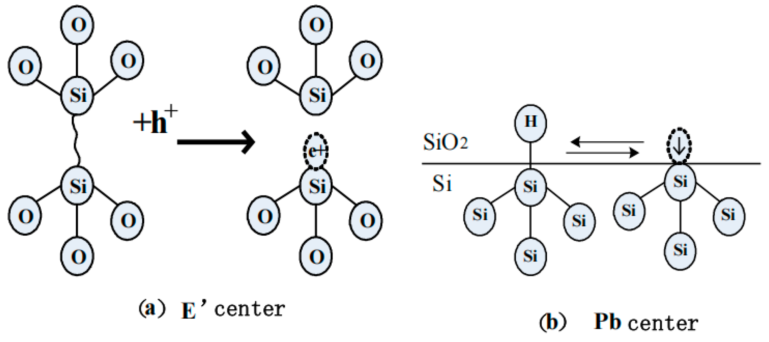
During TID irradiation of NMOS devices, the structural degradation of the gate oxide layer near the Si-SiO2 interface initiated with the dissociation of Si-Si bonds, creating dangling bonds that preferentially trapped holes to form E’ centers (Figure 8a). These E’ centers functioned as stable positive oxide trap charges due to their unpaired electrons localized at oxygen vacancy sites. Subsequent hot-carrier injection testing revealed a dynamic interplay between these trapped holes and injected hot electrons: the energetic electrons neutralized the trapped holes in dangling bonds, leading to a net reduction in positive charge within the oxide layer. This charge imbalance directly contributed to a measurable positive shift in threshold voltage, reflecting the cumulative impact of oxide trap charge modulation on device electrostatics.
Concurrently, TID irradiation triggered the transformation of silicon dangling bonds at the Si-SiO2 interface into Pb centers (Figure 8b), which exhibited amphoteric trapping behavior. These centers preferentially captured electrons under operational bias, generating negative interface trap charges. Intriguingly, the radiation-induced oxide trap charges displayed non-monotonic evolution during HCI testing, characterized by partial annihilation of trapped holes followed by charge inversion to negative polarity. Similarly, the interface trap charge density exhibited a bimodal trajectory: initial reduction due to recombination of electron–hole pairs with oxide traps near the interface during early HCI stages, succeeded by progressive accumulation as source-injected electrons became trapped by interface defects. The synergistic effect induced by TID and HCI stresses led to dual-phase evolution of oxide traps and interface traps, where the negative oxide trap charges and negative interface trap charges collectively amplified the positive threshold voltage shift through electrostatic coupling across the gate dielectric.
To elucidate the distinct contributions of oxide trap charges (Qot) and interface trap charges (Dit), comparative analysis of subthreshold swing (SS) degradation kinetics under hot-carrier stress is conducted on irradiated and non-irradiated devices (Figure 9). The subthreshold current can be expressed by the following [17]:
I D = I D 0 exp q ψ s nk T 1 exp q V D k T
where VG is the gate–source voltage, VD is the drain–source voltage, ID0 is the channel current when VG is equal to Vth, ψs is the surface potential, and n is the body factor which can be expressed by the following:
n = C o x + C d + C i t C o x
where Cox is the gate oxide capacitance per unit area, Cd is the depletion capacitance per unit area, and Cit is the interface trap capacitance per unit area.
So, the subthreshold swing can be expressed by the following:
S S ln 10 d V G d ( ln I D )
By substituting Equations (7) and (8) into Equation (9) for calculation, the subthreshold swing (SS) can be expressed as follows:
S S = k T q ln 10 ( 1 + C d + C i t C o x )
Since Cit = q2 × Dit, where Dit is interface trap density, it can be considered that the SS is a function of the interface trap density according to Equation (11).
However, Figure 9 demonstrates negligible differences in SS degradation patterns between irradiated and pristine devices, accompanied by minimal variations in Dit evolution during HCI testing. This critical observation conclusively demonstrates that the pronounced hot-carrier lifetime reduction caused by TID radiation predominantly stems from oxide trap charge dynamics (Qot) rather than interface trap charge accumulation. The mechanistic dominance of Qot is further corroborated by the charge inversion phenomena and sustained negative charge buildup in the oxide layer, which directly modulates carrier transport and enhances local electric fields, thereby accelerating device degradation under hot-carrier stress conditions.
The calculation formula for the saturation drain current is as follows [17]:
I D sat = 1 2 μ n C ox W L ( V G V th ) 2
where μn is electron mobility; W/L is the width-to-length ratio.
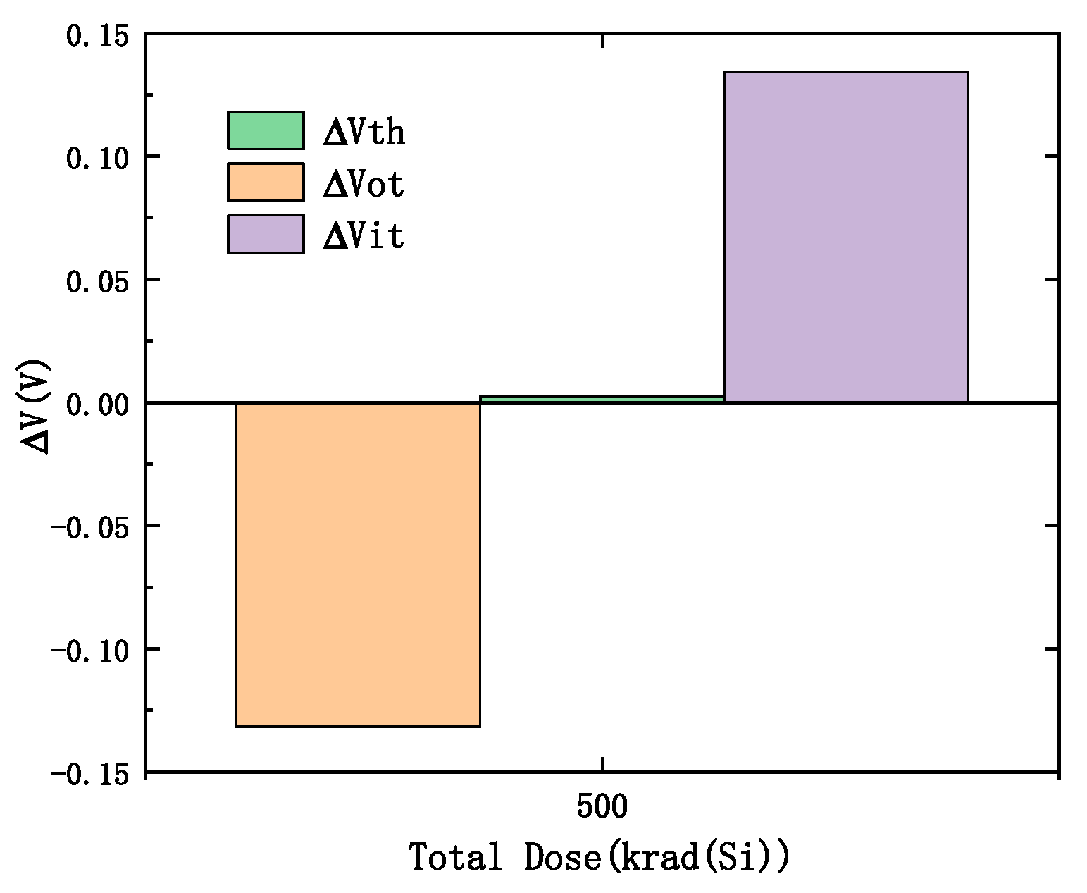
Although the total dose irradiation causes only a minor threshold voltage shift, radiation induces positive oxide trap charge and negative interface trap charge. To separate these two effects, the flat band voltage method [18] was employed. The threshold voltage shift (ΔVot) caused by the oxide trap charge and the threshold voltage shift (ΔVit) caused by the interface trap charge are presented in Figure 10. As can be observed from the figure, despite the total dose irradiation resulting in a small threshold voltage shift of 2.6 mV, ΔVot is −0.131 V and ΔVit is 0.134 V. This indicates that the induced oxide trap charge and interface trap charge counteract each other in terms of voltage.
The formation of oxide trap charges within the gate dielectric layer under total ionizing dose irradiation enhances Coulomb scattering events between charge carriers and lattice defects, significantly increasing the collision probability and degrading electron mobility through two mechanisms: (1) direct momentum transfer via charged defect scattering and (2) modification of the inversion layer charge density. However, during prolonged HCI testing, the injected high-energy electrons penetrate the oxide layer and undergo recombination with trapped holes in radiation-induced defects, partially neutralizing the positive oxide trap charges and even inducing charge inversion at certain defect sites where trapped holes are replaced by electrons. This dynamic charge compensation process reduces the net positive oxide trap charge density in irradiated devices to levels marginally below those observed in pristine devices under identical stress conditions, paradoxically resulting in less severe electron mobility degradation within the irradiated oxide layer.
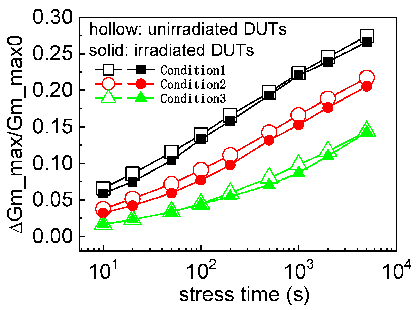
Since electron mobility varies less in irradiated devices compared to unirradiated devices, this also results in a similar pattern for the maximum transconductance (Gm-max). Figure 11 shows the variation in the ratio between the change in subthreshold maximum transconductance (ΔGm-max) and the pre-stress maximum transconductance (Gm-max0) with stress time under three hot-carrier injection stress conditions. It can be seen from the figure that all three HCI stress conditions exhibit a consistent trend: the ΔGm-max/Gm-max0 value for irradiated devices is smaller than that for unirradiated devices.
The maximum transconductance in the subthreshold region is expressed as follows [17]:
G m max = I D V G μ n C OX W L V D
As shown in Equation (13), when VD is fixed, Gm-max depends linearly on electron mobility. Due to mobility degradation in irradiated devices, unirradiated devices exhibit lower ΔIDsat values compared to irradiated ones. This behavior contrasts with the ΔVth trend, ultimately leading to a significantly extended lifetime of irradiated devices in hot-carrier stress tests compared to unirradiated counterparts.
Consequently, irradiated NMOS devices exhibit smaller electron mobility variations (Δμn) in the gate oxide region compared to non-irradiated devices during HCI stress, as the radiation-modified defect population provides both trap sites for charge neutralization and recombination centers that mitigate scattering effects. This counterintuitive behavior directly correlates with the observed degradation patterns in ΔIDsat, confirming that IDsat degradation kinetics are predominantly governed by electron mobility changes rather than threshold voltage shifts under these coupled radiation–HCI stress conditions. The experimental validation of this mechanism through parameter extraction and defect spectroscopy aligns with theoretical models describing defect–charge interaction dynamics in irradiated MOS systems, establishing a comprehensive framework for understanding reliability degradation in radiation-hardened devices subjected to combined environmental stresses.

4. Conclusions

This study reveals the dual-effect mechanism of total ionizing dose (TID) radiation on HCI reliability in NMOS devices. Experimental data demonstrate accelerated threshold voltage shift in irradiated devices under specific HCI stress conditions, while the degradation of saturation drain current shows a deceleration trend. Quantification using the IEC 62416-2010-based degradation model indicates that when ΔVth = 50 mV is set as the failure criterion, the HCI lifetime of irradiated devices (1.330 × 10¹¹ s) decreases to 65% of non-irradiated counterparts. Conversely, with ΔIDsat = 0.6 mA as the criterion, the HCI lifetime of irradiated devices (5.835 × 10¹⁰ s) doubles compared to non-irradiated ones.
This paradoxical behavior stems from fundamentally distinct physical mechanisms activated by total ionizing dose (TID) radiation: During hot-carrier injection (HCI) stress, the partial neutralization (30–40% recombination efficiency) of positive charges trapped in E’ centers—created by radiation-induced rupture of strained Si-Si bonds at the oxide interface—disrupts the localized electric field screening previously maintained by these trapped holes. The resultant electric field intensification near the gate edge accelerates high-energy carrier injection into the oxide, forming positive feedback that amplifies threshold voltage drift through two interrelated pathways—enhanced trap-assisted tunneling and increased charge trapping probability at radiation-modified defect sites. Conversely, interface traps exhibit diminished contributions to degradation due to thermally activated self-recovery mechanisms during HCI stress, where elevated temperatures facilitate defect annealing and recombination of trapped charges, effectively “healing” a portion of radiation-induced interface states. This annealing-driven recovery suppresses interface trap charge accumulation, decoupling ΔIDsat degradation from threshold voltage shifts and instead tethering saturation current reduction primarily to electron mobility degradation governed by scattering dynamics. Crucially, the mobility degradation demonstrates an inverse proportionality to oxide trap charge neutralization efficiency—as trapped holes in E’ centers are progressively neutralized by hot electrons, the resultant reduction in Coulomb scattering centers temporarily mitigates electron mobility loss despite the ongoing ΔVth drift. These dual mechanisms collectively reveal a competitive interplay between oxide trap charge modulation and electron mobility driven transport degradation, establishing a predictive model where ΔVth scales with trapped charge neutralization kinetics while ΔIDsat correlates with defect scattering cross-section evolution. The identification of this decoupled degradation paradigm provides critical insights for radiation-hardened circuit co-design, enabling simultaneous optimization of threshold voltage stability and drain current retention through strategic balancing of oxide defect passivation techniques and electron mobility-enhancing channel engineering, ultimately advancing the development of dual stress-tolerant integrated circuits for extreme radiation environments.

Author Contributions

Conceptualization, R.G.; validation, T.M.; formal analysis, X.Z. (Xiaowen Zhang); data curation, X.Z. (Xianyu Zhang); writing—original draft, Y.H.; writing—review and editing, Y.Y. All authors have read and agreed to the published version of the manuscript.

Funding

This research was funded by Guangdong S&T Program (grant No. 2022B0701180002) and Young Scientists Fund of the National Natural Science Foundation of China (Grant No. 62204061).

Data Availability Statement

The original contributions presented in this study are included in the article. Further inquiries can be directed to the corresponding author.

Conflicts of Interest

Authors Yujuan He, Rui Gao, Teng Ma, Xiaowen Zhang, and Xianyu Zhang were employed by the company Science and Technology on Reliability Physics and Application of Electronic Component Laboratory, China Electronic Product Reliability and Environmental Testing Research Institute. The remaining authors declare that the research was conducted in the absence of any commercial or financial relationships that could be construed as a potential conflict of interest. We declare that we have no known competing financial interests or personal relationships that could have appeared to influence the work reported in this paper entitled “Total Ionizing Dose Effects on Lifetime of NMOSFETs Due to Hot-Carrier-Induced Stress”.

References

  1. Oldham, T.R.; McLean, F.B. Total ionizing dose effects in MOS oxides and devices. IEEE Trans. Nucl. Sci. 2003, 50, 483–499. [Google Scholar] [CrossRef]
  2. Zheng, Z.; Zhao, X.; Zhao, K.; Gao, J.; Li, B.; Yu, F.; Li, B.; Luo, J.; Han, Z.; Liu, X. Comparison of the Total Dose Responses of Fully Depleted SOI nMOSFETs With Different Geometries for the Worst Case Bias Conditions. IEEE Trans. Nucl. Sci. 2019, 66, 2207–2214. [Google Scholar] [CrossRef]
  3. Fleetwood, D.M.; Xiong, H.D.; Lu, Z.Y.; Nicklaw, C.J.; Felix, J.A.; Schrimpf, R.D.; Pantelides, S.T. Unified model of hole trapping, 1/f noise, and thermally stimulated current in MOS devices. IEEE Trans. Nucl. Sci. 2002, 49, 2674–2683. [Google Scholar] [CrossRef]
  4. Chenming, H.; Simon, C.T.; Fu-Chieh, H.; Ping-Keung, K.; Tung-Yi, C.; Terrill, K.W. Hot-electron-induced MOSFET degradation—Model, monitor, and improvement. IEEE Trans. Electron Devices 1985, 32, 375–385. [Google Scholar] [CrossRef]
  5. Heremans, P.; Bellens, R.; Groeseneken, G.; Maes, H.E. Consistent model for the hot-carrier degradation in n-channel and p-channel MOSFETs. IEEE Trans. Electron Devices 1988, 35, 2194–2209. [Google Scholar] [CrossRef]
  6. Cui, J.-W.; Yu, X.-F.; Ren, D.-Y.; Lu, J. The influence of channel size on total dose irradiation and hot-carrier effects of sub-micro NMOSFET. Acta Phys. Sin. 2012, 61, 026102. [Google Scholar] [CrossRef]
  7. Silvestri, M.; Gerardin, S.; Paccagnella, A.; Faccio, F. Degradation Induced by X-Ray Irradiation and Channel Hot Carrier Stresses in 130-nm NMOSFETs With Enclosed Layout. IEEE Trans. Nucl. Sci. 2008, 55, 3216–3223. [Google Scholar] [CrossRef]
  8. Arora, R.; Fleetwood, Z.E.; Zhang, E.X.; Lourenco, N.E.; Cressler, J.D.; Fleetwood, D.M.; Schrimpf, R.D.; Sutton, A.K.; Freeman, G.; Greene, B. Impact of Technology Scaling in sub-100 nm nMOSFETs on Total-Dose Radiation Response and Hot-Carrier Reliability. IEEE Trans. Nucl. Sci. 2014, 61, 1426–1432. [Google Scholar] [CrossRef]
  9. Ren, D.-Y.; Yu, X.-F.; Erkin. The relationship between hot-carrier damage and ionizing radiation damage in MOS capacitors. Res. Prog. SSE. 2001, 21, 103–108. (In Chinese) [Google Scholar]
  10. He, Y.-J.; Zhang, X.-W.; Liu, Y. Total Dose Dependence of Hot Carrier Injection Effect in the NMOS Devices. Acta Phys. Sin. 2016, 65, 246101. (In Chinese) [Google Scholar] [CrossRef]
  11. Xie, R.; Qiao, M.; Zhou, X.; Ge, C.; Xu, S.; Hong, G. The Correlation of Total Dose Effect and Hot Carrier Injection for Radiation Hardened MOS. In Proceedings of the 2022 10th International Symposium on Next-Generation Electronics (ISNE), Wuxi, China, 22–23 October 2022. [Google Scholar] [CrossRef]
  12. Yogi, P.; Kumar, M.; Aditya, K.; Gupta, C.; Dixit, A. Impact of Hot Carrier Injection on Total Ionizing Dose Effect of 10-nm N-channel Bulk FinFETs. In Proceedings of the 2020 5th IEEE International Conference on Emerging Electronics (ICEE), New Delhi, India, 26–28 November 2020; pp. 1–4. [Google Scholar]
  13. Zheng, Q.; Cui, J.; Yu, X.; Li, Y.; Guo, Q. Anneal Behavior of Total Ionizing Dose Irradiated UTBB FD-SOI n-MOSFETs Activated by Hot Carrier Stress. IEEE Trans. Nucl. Sci. 2023, 70, 37–43. [Google Scholar] [CrossRef]
  14. Yao, R.; Lu, H.; Zhang, Y.; Zhang, Y.; Qiao, J.; Sun, J.; Xun, M.; Yu, G. Influence of Hot Carrier Degradation on Total Ionizing Dose in Bulk I/O-FinFETs. IEEE Trans. Device Mater. Reliab. 2024, 24, 456–462. [Google Scholar] [CrossRef]
  15. Ren, Z.; An, X.; Li, G.; Liu, J.; Xun, M.; Guo, Q.; Zhang, X.; Huang, R. TID Response and Radiation-Enhanced Hot-Carrier Degradation in 65-nm nMOSFETs: Concerns on the Layout-Dependent Effects. IEEE Trans. Nucl. Sci. 2021, 68, 1565–1570. [Google Scholar] [CrossRef]
  16. BS EN 62416:2010; IEC 62416-2010 Standard: Semiconductor Devices-Hot Carrier Test on MOS Transistors. International Electrotechnical Commission (IEC): Geneva, Switzerland, 2010.
  17. Sze, S.M.; Kwok, K.N. Physics of Semiconductor Devices; A JOHN WILEY & SONS, JNC. PUBLICATION: Hoboken, NJ, USA, 2006; pp. 293–373. [Google Scholar] [CrossRef]
  18. McWhorter, P.J.; Winokur, P.S. Simple technique for separating the effects of interface traps and trapped-oxide charge in metal-oxide-semiconductor transistors. Appl. Phys. Lett. 1986, 48, 133–135. [Google Scholar] [CrossRef]
Figure 1. Transfer characteristic curves (ID-VG curves) before and after irradiation and annealing.
Electronics 14 02563 g001
Figure 2. (a) Vth, (b) Gm-max (c) SS distribution of DUTs before radiation, after 500 krad radiation and after annealing.
Electronics 14 02563 g002
Figure 3. ID-VG curves of sample with HCI test.
Electronics 14 02563 g003
Figure 4. Threshold voltage during irradiation, annealing, and HCI tests.
Electronics 14 02563 g004
Figure 5. Variations in NMOSFET parameter drift under three hot-carrier injection stress conditions with stress duration: (a) threshold voltage shift and (b) saturation drain current shift.
Electronics 14 02563 g005
Figure 6. Threshold voltage shifts in the NMOSFET devices measured and predicted from the power law model (a) before and (b) after irradiation.
Electronics 14 02563 g006
Figure 7. Saturation drain current shifts in the NMOSFET devices measured and predicted from the power law model (a) before and (b) after irradiation.
Electronics 14 02563 g007
Figure 8. The trap centers: (a) E’ center; (b) Pb center.
Electronics 14 02563 g008
Figure 9. ΔSS/SS0 of HCI tests between irradiated and unirradiated NMOSFET.
Electronics 14 02563 g009
Figure 10. The values of ΔVth, ΔVot, and ΔVit after irradiation with a total dose of 500 krad (Si).
Electronics 14 02563 g010
Figure 11. ΔGm-max/Gm-max0 of HCI tests between irradiated and unirradiated NMOSFET.
Electronics 14 02563 g011
Table 1. The test condition of samples.
HCI Stress ConditionVD/VVG/VVS/VVsub/V
Condition 12.71.800
Condition 22.51.700
Condition 32.31.600
Disclaimer/Publisher’s Note: The statements, opinions and data contained in all publications are solely those of the individual author(s) and contributor(s) and not of MDPI and/or the editor(s). MDPI and/or the editor(s) disclaim responsibility for any injury to people or property resulting from any ideas, methods, instructions or products referred to in the content.

