Article

A Novel Two-Stage Power Conversion Method Suitable for 1MHz-LDC of Electric Vehicles †

School of Electrical Engineering, Soongsil University, Seoul 06978, Republic of Korea
*
Author to whom correspondence should be addressed.
This paper is an extended version of our paper published in the Proceedings of the 2019 ICPE-ECCE Asia Conference, Busan, 27–31 May 2019.
Electronics 2025, 14(12), 2403; https://doi.org/10.3390/electronics14122403
Submission received: 7 May 2025 / Revised: 9 June 2025 / Accepted: 10 June 2025 / Published: 12 June 2025

Abstract

:
Low-Voltage DC-DC converters (LDCs) in electric vehicles require high power density and high efficiency operation over the wide range of load and input voltage variations. This paper introduces a novel topology which combines three 1 MHz half-bridge (HB) LLC resonant converters and an inverting buck–boost (IBB) converter to adjust the output voltage without frequency modulation. The switching frequency of the proposed converter is fixed at 1 MHz to achieve a constant frequency operation for the resonant converter. In the proposed topology, Gallium Nitride (GaN) devices and planar transformers are employed to optimize the converter operation at high frequency. A 1-MHz/1.8 kW-400/14 V prototype converter is built to verify the feasibility and the validity of the proposed LDC topology.

1. Introduction

As the automotive industry moves toward EVs, there is an increasing demand for systems that combine high efficiency and strong power density. The LDC in an EV’s standard power system is important because it helps move power from the high-voltage (HV) DC bus to the low-voltage (LV) DC bus. This means it supplies electricity for lights, control units and extra equipment, as represented in Figure 1 [1,2,3,4,5]. Because these converters are integrated into vehicles, modern LDCs must deliver compact size alongside high performance. One prevalent approach to reducing converter size involves increasing the switching frequency. However, this introduces a trade-off, as higher switching frequencies typically lead to increased switching losses, thereby lowering efficiency. Consequently, designing high-frequency LDCs presents several challenges, particularly in balancing compactness and energy efficiency while still achieving critical performance metrics such as wide input voltage range, significant step-up/down capability, and stable load regulation. Due to its high-frequency operation, the LLC resonant DC-DC converter is considered unique among other types of converters. The ability to use soft-switching for both the primary and secondary switches enables the system to adapt to different load conditions [6,7,8,9].
As the LLC converter uses the transformer’s leakage inductance, it is possible to reduce the need for magnetic items in the circuit. Despite its many favorable features, the LLC converter has a notable drawback: it struggles to maintain resonant operation under varying input voltages and load conditions. This undermines its key strength: operating at high efficiency. For the converter to be suitable for demanding automotive applications like LDCs, several challenges must be addressed. These include handling a wide range of input voltage fluctuations, achieving a high step-down voltage gain to support extremely high output currents, managing frequency variations, and ensuring reliable synchronous rectification. Addressing these issues adds significant complexity to both the control strategy and the circuit design.
This paper presents a novel two-stage power conversion architecture tailored for Low-Voltage DC-DC (LDC) applications in electric vehicles. To overcome the major limitations of conventional LLC converters, a cascoded front-end inverting buck–boost (IBB) converter is introduced to stabilize the input voltage to the LLC stage. In the second stage, three LLC series resonant converters (LLC-SRCs) are connected in parallel to ensure constant output voltage regulation and to support high output current demand. Unlike traditional two-stage DC-DC topologies, where the entire input power is processed through both stages, the proposed design directs most of the power directly to the LLC stage. Only a small portion of the power passes through the IBB converter, just enough to regulate the LLC input, which significantly reduces power conversion losses. The LLC converter operates at a constant switching frequency of 1 MHz, eliminating the need for complex control methods or extra circuitry to drive the synchronous rectifiers (SRs) [10,11,12].
In typical LDC systems, the output current is high due to the substantial step-down voltage ratio. In this design, the rated output current is 130 A at an output power of 1.8 kW. To mitigate the current stress on the rectifier MOSFETs, the three LLC converters are configured in parallel so that each one delivers approximately 600 W. Current balancing on the secondary side is achieved using a passive common capacitor approach [13], removing the need for intricate current sensing and control algorithms [14,15,16]. Gallium Nitride (GaN) MOSFETs are employed as primary switches in the LLC stage owing to their superior static and dynamic characteristics, which enable high-frequency operation with minimal switching loss. Their low output capacitance and low gate charge make them especially suitable for MHz-range applications [17,18,19,20]. To verify the proposed topology, a 1.8 kW (400 V/14 V) prototype DC-DC converter is developed and validated through both simulations and experimental results.

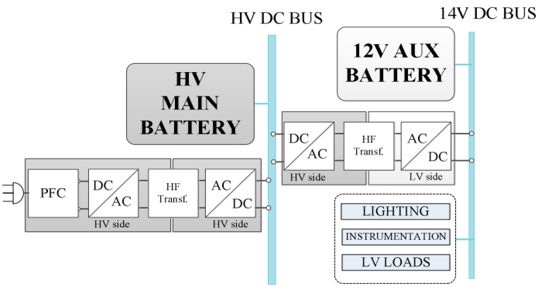
2. Operating Principle of the Proposed Converter

2.1. Brief Introduction of Operating Principle

The schematic of the proposed converter is shown in Figure 2. The system contains an inverting buck–boost stage, and three LLC stages laid out in parallel. The synchronous IBB converter works in a loop to include regulation of the output voltage. Three half-bridge LLC converters are organized in parallel to ensure equal distribution of the 1.8 kW output power. To efficiently manage the high output current, synchronous rectifiers (SRs) are employed, which help to minimize conduction losses and thermal stress.
However, if the switching frequency changes dynamically based on variations in input voltage or load conditions, it becomes difficult to generate proper PWM signals for the SRs. This is because the PWM signals on the secondary side may no longer align in phase with those on the primary side, requiring complex circuitry and control algorithms. On the other hand, by fixing the switching frequency of the LLC converters, a simpler PWM generation method can be utilized to drive both primary and secondary side switches, as demonstrated in Figure 3. Additionally, to counteract the effects of component tolerance within each resonant tank, a passive impedance matching technique is incorporated [13].
Figure 3 illustrates the main waveforms of the proposed LDC converter throughout a full switching cycle. The signals VS1, VS3, and VS5 (from top to bottom) correspond to the gate–source voltages of the high-side MOSFETs, while VS2, VS4, and VS6 denote those of the low-side MOSFETs in each of the three parallel LLC converter stages. The waveforms Vds_S2, Vds_S4, and Vds_S6 depict the drain-to-source voltages of the low-side switches, which also serve as the input voltages to the respective resonant tanks. The resonant currents (iPri1, iPri2, iPri3) and magnetizing currents (iLm1, iLm2, iLm3) are shown next, representing the behavior within each resonant stage.
The currents flowing through the synchronous rectifiers, denoted as ids_Q1 through ids_Q6, indicate the drain–source currents of the SR MOSFETs. At the bottom of the waveform set, the gate–source voltages (VQ1 to VQ6) are shown, corresponding to the control signals driving the SRs. As previously discussed, there is no phase shift between the control signals of the primary and secondary switches. This alignment greatly simplifies the PWM signal generation, thereby reducing both the overall control complexity and the associated system cost.

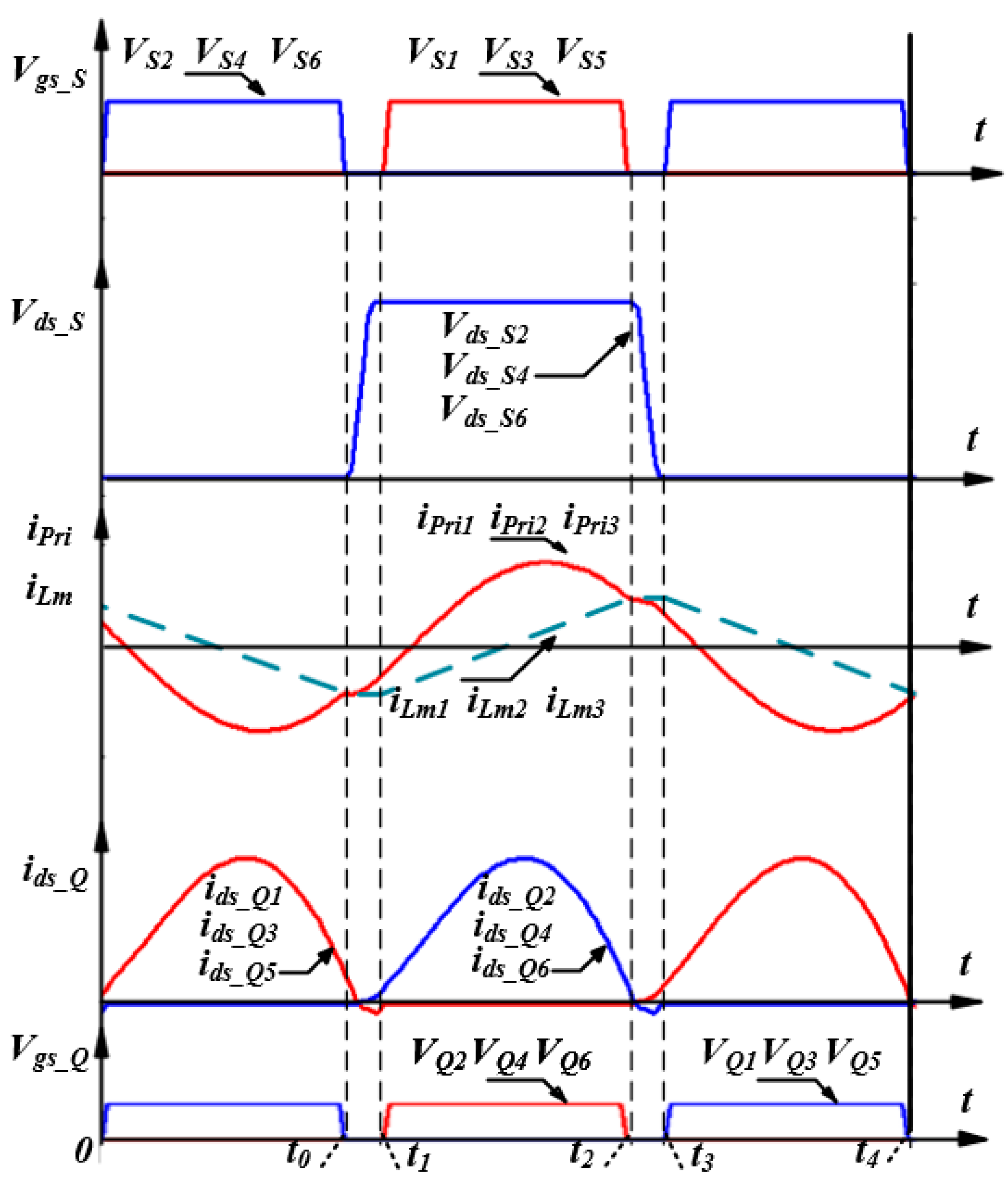
2.2. Operating Principle

The proposed converter architecture can be represented in a simplified form, as shown in Figure 2b. In this configuration, the main high-voltage (HV) battery is connected in a cascoded arrangement with the conventional IBB circuit to enable efficient energy transfer.
V i n = V B a t V I b b = V B a t ( 1 + D 1 D )
The input voltage to the LLC converter in the suggested topology is calculated by adding the HV battery voltage and the output voltage from the IBB converter, following Equation (1). Here, V Bat is the voltage of the high-voltage battery, V IBB is the result we get from the IBB stage, and D helps us define the IBB converter’s duty cycle. To study the DC gain features of the LLC stage, the FHA approach is used, and the model is given in Figure 4.
With leakage inductance considered, the voltage conversion ratio of the LLC stage is calculated using Equation (2).
M f r = 1 + L l k 2 L m 1 + j f n 2 Q k b 1 f n 2 1 f n 2 k a 1 + f n 2 1 1 f n 2 k a
Here, M denotes the voltage conversion ratio; L r is the resonant inductance; f n represents the normalized switching frequency; L m and L s are the magnetizing and secondary leakage inductances, respectively, used to define the inductance ratios L m L r and L s L r ; Q is the quality factor; Z c is the characteristic impedance; f r is the resonant frequency; and f s is the switching frequency. The equivalent load resistance reflected from the secondary to the primary side is denoted as R e q and can be calculated using the given relationship.
In the proposed converter topology, the switching frequency is set equal to the resonant frequency of the L r C r tank, and under this condition, the voltage gain of the LLC converter becomes M = 1. It is evident that at the resonant frequency, the gain remains constant regardless of load conditions. At lower switching frequencies, since the magnetizing inductance L m is significantly greater than the reflected secondary leakage inductance L s , the voltage gain M tends to be nearly unity. However, at higher switching frequencies such as 1 MHz, the impact of secondary-side leakage inductance becomes non-negligible, thereby affecting the DC gain characteristics of the LLC converter.
Using Equations (1) and (2), the overall voltage gain of the proposed converter can be derived and is presented in Equation (3).
G c = V 0 V b = 1 2 n 1 + L l k 2 L m 1 + D 1 D
As indicated in Equation (3), the voltage conversion gain of the proposed converter is primarily governed by the duty cycle of the PWM-controlled IBB converter. The output voltage is regulated through a closed-loop voltage control implemented on the IBB stage. Furthermore, as shown in Equation (3), the voltage conversion gain is also affected by the ratio between the secondary leakage inductance L l k 2 and the magnetizing inductance L m .

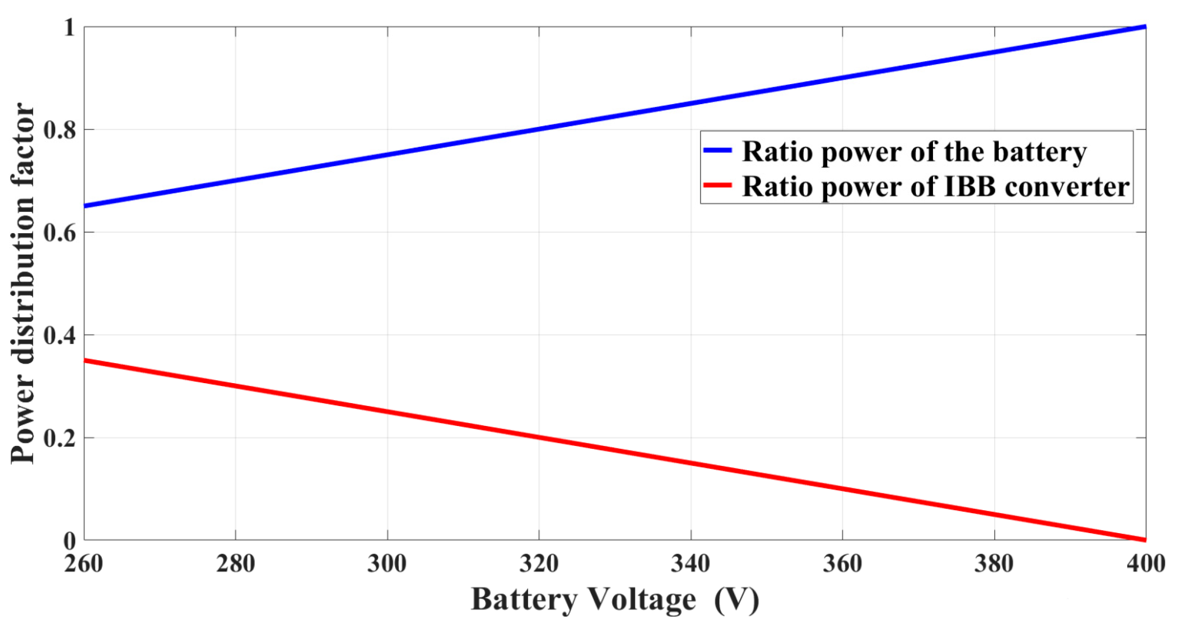
2.3. Power Flow Analysis

The block diagram of the suggested two-stage cascoded power-conversion architecture, along with its power flow and power distribution representations, is illustrated in Figure 5. In this configuration, an inverting buck–boost (IBB) converter is connected in series with the high-voltage (HV) battery to supply a constant input voltage to the LLC converters. Consequently, the IBB stage is responsible for providing only the voltage difference between the HV battery and the desired output voltage. Since the IBB converter processes only this differential voltage, its voltage and power ratings can be substantially lower. As previously discussed, the IBB converter operates such that the combined voltage of its output and the HV battery remains constant, ensuring a steady input for the LLC stages. The output voltage of the LLC converters is thus regulated indirectly by the closed-loop control applied to the IBB converter. Overall efficiency of the proposed topology is enhanced, as only a small portion of power—the differential power—is processed by the IBB converter, thereby reducing conversion losses.
As illustrated in Figure 5a, the efficiency E f of the cascoded system can be determined using the following equation:
E f = P O P B a t = I 0 × V B a t + I 0 × V I b b I 0 × V B a t + V I b b × I 0 E f _ i b b = 1 + V I b b / V B a t 1 + V I b b / V B a t E f _ i b b E f _ i b b
Here, V B a t and V I b b represent the output voltages of the battery and the IBB converter, respectively, while I o denotes the output current of the cascoded structure, and E E f _ i b b is the efficiency of the IBB converter. As evident from Equation (3), the overall efficiency E f of the proposed topology is theoretically higher than the efficiency of the IBB stage E f _ i b b . Moreover, a smaller voltage ratio V I b b / V B a t leads to an increase in the total system efficiency E f .
β 1 = P B a t P O V B a t V B a t + V I B B β 2 = P I B B P O V I B B V B a t + V I B B
The proportion of power supplied by the battery and the IBB is determined using Equation (5) and depicted in Figure 6. In this context, β1 and β2 represent the power contribution ratios of the battery and the IBB, respectively. Here, P B a t denotes the power delivered to the LLC stage by the high-voltage battery, while P I B B refers to the power provided to the same stage by the IBB DC-DC converter.

2.4. Load Current Balancing in Multiphase Parallel LLC Converters

A multiphase parallel LLC converter helps mitigate current stress by distributing the load power evenly across each phase. However, the resonant current in LLC converters is highly sensitive to changes in the switching frequency. Any deviation or mismatch in the resonant components across phases can result in current imbalance among the converters. To address this, a passive impedance matching approach, as introduced in [13], employs either common inductors or common capacitors. This method enables automatic current sharing among the phases without relying on complex control strategies, sensing circuits, or frequency modulation techniques.
I p r i 1 = I p r i 01 e j α ; I p r i 2 = I p r i 02 e j β ; I p r i 3 = I p r i 03 e j θ
V c = I p r i 1 R s 1 + I p r i 1 / ( j ω C r 1 ) = I p r i 2 R s 2 + I p r i 2 / ( j ω C r 2 ) = I p r i 3 R s 3 + I p r i 3 / ( j ω C r 3 )
I C = I p r i 1 + I p r i 2 + I p r i 3
Due to mismatches in component values, the resonant currents in each phase may become unequal, as illustrated in Figure 7a and Equation (6). To address this issue, capacitors C r 1 , C r 2 ,   a n d   C r 3 are introduced, as shown in Figure 2, to equalize the current distribution across the phases. These capacitors function similarly to virtual resistors, ensuring the condition in Equation (7) is met. The effective impedance introduced by these virtual resistors can be either positive or negative, compensating for the resonant current imbalance, as demonstrated in Figure 7b–d. Consequently, the output current on the secondary side becomes fully balanced.

3. Design Considerations

This section outlines a simplified design methodology for the prototype LDC, based on the following specifications (Table 1):

3.1. IBB Stage Parameter Design

As illustrated in Figure 4 and derived from Equation (6), the power contribution from the HV battery remains consistently higher than that of the IBB stage across the battery voltage range of 260–400 V. Consequently, the power rating of the IBB stage is determined using Equation (9):
P I B B = β 2 m a x × P O     650   W
The output voltage range of the IBB stage is governed by the variation in the HV battery input voltage and can be determined using Equation (6):
V I B B = β 2 × V B a t 1 β 2
To ensure continuous conduction mode (CCM) operation at a light load of 10%, the IBB stage is designed accordingly. The maximum allowable inductance L 1 is derived from Equation (7) to guarantee that the inductor current remains above zero under 10% load conditions.
L 1 = ( 1 D ) 2 × V I B B × 10 % 2 × f S W × I O _ I B B
Table 2 summarizes the essential design parameters of the IBB stage.

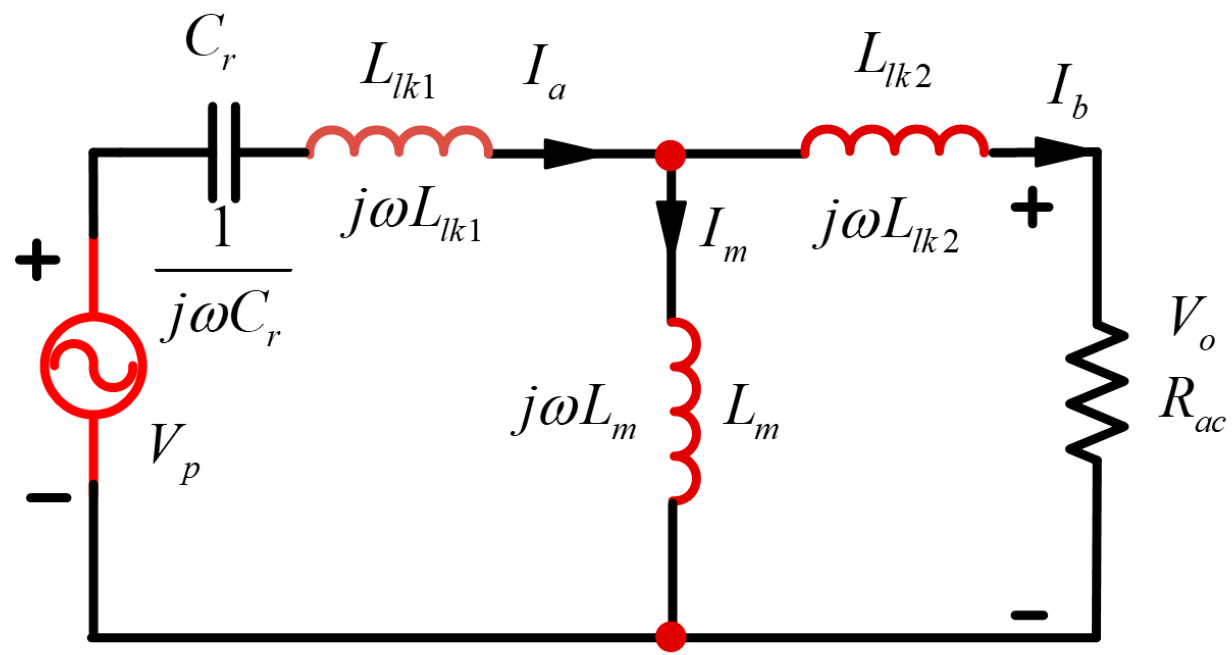
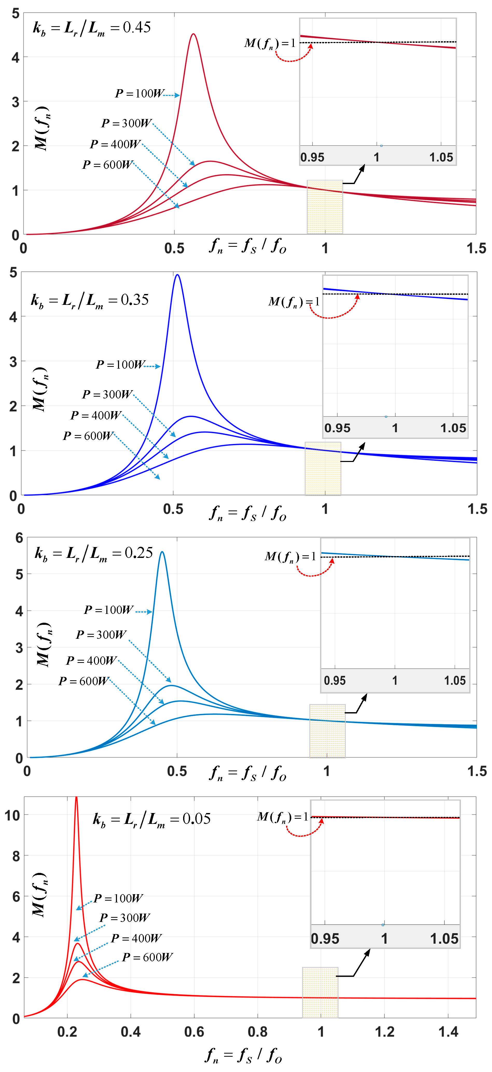
3.2. LLC Parameters Design

Usually, a conventional approach to using low input voltage in LLC converters reduces the magnetizing inductance. However, even a little magnetizing inductance brings up several difficulties:
  • As the magnetizing current constitutes a substantial portion of the total resonant current, the reactive power increases, thereby deteriorating the power factor.
  • Elevated magnetizing current results in higher turn-off current through the primary switches, which in turn increases the switching losses.
Consequently, the efficiency of the LLC converter is seriously compromised. In the proposed LDC converter, output voltage regulation is taken away from the LLC stage. Thus, it becomes unnecessary to use a large magnetizing current. The magnetizing inductance L m can therefore be designed with a higher value to reduce the magnetizing current, while still ensuring that it remains sufficiently large to maintain zero-voltage switching (ZVS) for the primary switches during the dead-time interval. For low output voltage, high output current in LDC design, parallel synchronous rectifiers are mandatory to reduce secondary side conduction loss. As a result, magnetizing current need discharge not only intrinsic capacitance on primary switches but also reflected intrinsic capacitance from secondary side switches, as well as transformer winding capacitances. Therefore, ZVS condition can be given in (12).
Q m a g 2 . C p r i _ o s s V i n + C w i n d . V i n + 1 n 2 . 2 N C sec _ o s s . 2 V o
where Cpri_oss and Csec_oss are the output capacitance of primary switches and secondary switches, respectively, Cwind is the winding capacitance of the transformer, N is the number of parallel SRs, n is the ratio between the number of turns in the windings, and Qmag is the total charge generated by magnetizing energy stored in Lm, which can be calculated by (13):
Q m a g = i L m _ m a x t d e a d
where iLm_max is the peak magnetizing current, which can be calculated as
i L m _ m a x = n V o ( T s t d ) 2 . L m
Required magnetizing inductance Lm can be derived in (15) by substituting (13) and (14) into (12):
L m = t d e a d ( T s / 2 t d e a d ) 4 ( 2 . C p r i _ o s s + ( 1 / n 2 ) .2 N . C sec _ o s s + C w i n d )
where TS is the switching time period, tdead is the needed dead time. According to (15), the optimal magnetizing inductance depends on the dead time, then Lm can be determined with the selected dead time value. The selection of L m and the dead time t dead involves a trade-off to optimize efficiency. Once L m is chosen, the corresponding resonant inductance L r must be carefully determined.
The relationship between voltage gain and operating switching frequency under various load conditions, with different values of the coefficient k b (0.45, 0.35, 0.25, and 0.05), is illustrated in Figure 8. In the proposed converter topology, the quality factor Q e is not a critical design consideration, as the switching frequency is fixed at the resonant frequency f 0 . It is important to ensure that the voltage gain remains close to unity around the resonant frequency f 0 , irrespective of variations in load or resonant frequency. This design approach reduces the sensitivity of the output voltage of each LLC converter phase to component mismatches.
As demonstrated in Figure 8, minimizing the coefficient k b results in a lower leakage inductance value, assuming L r L l k 1 (neglecting the influence of L l k 2 ). By designing a transformer with minimal leakage inductance, load current sharing among the parallel LLC converter phases is enhanced. Any remaining minor current imbalance can be effectively corrected using the passive current sharing technique.
The next section addresses the transformer design strategy aimed at achieving a low leakage inductance. Given that the leakage inductance functions as the resonant inductance L r , the corresponding resonant capacitor can be calculated accordingly.
C r = 1 ( 2 π . f r ) 2 L r = 1 ( 2 π . f r ) 2 L l k 1
Here, f r represents the selected resonant frequency, and C r denotes the resonant capacitance.

3.3. Planar Transformer Design Consideration

The benefits of planar transformers include a low design height, reduced leakage, extra cooling and consistent operation. That is why planar transformers are perfect for low profile uses such as in electric vehicles. Consequently, the use of a planar transformer is incorporated in the proposed LDC converter. The transformer is the central element for high frequency, high step-down, and high output current LLC resonant converters. The way the transformer works determines the converter’s running and efficiency, since the transformer usually accounts for the highest percentage of converter loss. In the proposed LDC converter, 1.8 kW power is transferred to the output through three planar transformers as the following specifications (Table 3).
The conventional planar transformer structure exposes many drawbacks in high power, high-frequency applications as applied in the proposed LDC converter. Two serious problems of conventional PL are easily realized:
(1)
Planar transformers suffer from high parasitic capacitance; the effects of parasitic capacitance have been discussed in several studies [21,22,23,24]. Overlapping PCB trace and high voltage gradient is the main reason which creates the parallel plate capacitors. Equation (16) shows that the higher parasitic winding capacitance requires higher magnetizing current at the transformer input, resulting in a higher loss. In addition, high intra-winding capacitance of planar transformer distorts the waveforms and impacts the voltage conversion ratio and light load regulation [23,24].
(2)
When using a traditional planar transformer with low frequency and low output, the copper poles of the main PCB are generally used to connect the added-side windings. But, this arrangement suffers greatly from termination losses because of proximity effect and skin effect, which leads to most of the current being near the edges. This results in high heat and more losses around the edge terminals. The key reason behind this problem is that it leads to noticeable power loss in the high-power, high-frequency planar transformer [25].
An improvement on traditional design is seen in [26], since PCB layers act as secondary windings and both the SRs and the output capacitors are connected on the same PCB layer to reduce power loss at the terminals. On the other hand, this structure carries previous parasitic winding capacitance. The use of the matrix transformer has the benefit of boosting the output current power by distributing secondary winding current over several cores [27,28,29]. Also, this design eliminates loss from AC cutoff due to including the secondary RC part into the secondary winding. While it delivers strong performance and uses less space, this electric motor often requires multiple magnetic cores or special cores and multi-layer PCB winding which makes the structure complex and pricey.
In proposed LDC converter, the PL-TRs are designed to be able to address two earlier mentioned problems of conventional PL-TR and compromise among the complexity, cost and efficiency. The structure of the proposed transformer is described as in Figure 9. For low-voltage and high-current LLC converter, the center-tapped transformer structure is usually chosen. Because the secondary-side winding conducts for only half of the switching period, the center-tapped winding must be designed as symmetrically as possible to prevent any circuit imbalance.
As mentioned in Section 2.3, interleaving primary and secondary windings is the most effective method to reduce the leakage inductance for enhancing passive current sharing capability. As depicted in Figure 9a, the interleaving structure can be achieved, but a large overlapping winding layout induces a large amount of parasitic capacitance [24]. In Figure 9b, a minimized-overlapping winding layout is proposed by winding 16 turns of primary clockwise for the first set of interleaving structure and anticlockwise for the second set, and finally stacking both sets to form the winding structure. The number of sets can be extended to entirely fill the window core. For the secondary side, a number of parallel SRs are a must to reduce the current conduction loss. As a result, attaching the SRs and output filter capacitors to each secondary winding eliminates high-frequency AC current at the connections with the power board. There is no issue of parallel multiple SRs because each SR attached in secondary side conducts the current independently. Compared to placing SRs on the power board, the large loop of secondary side is significantly minimized. As a result, the oscillating on secondary side switches and the effects of secondary winding leakage can be further suppressed. The number of SRs used in one planar transformer are decided by compromising between conduction loss and driving loss. A higher number of SRs results in lower conduction loss but higher driving loss. The number of SRs used in the proposed design is 8.

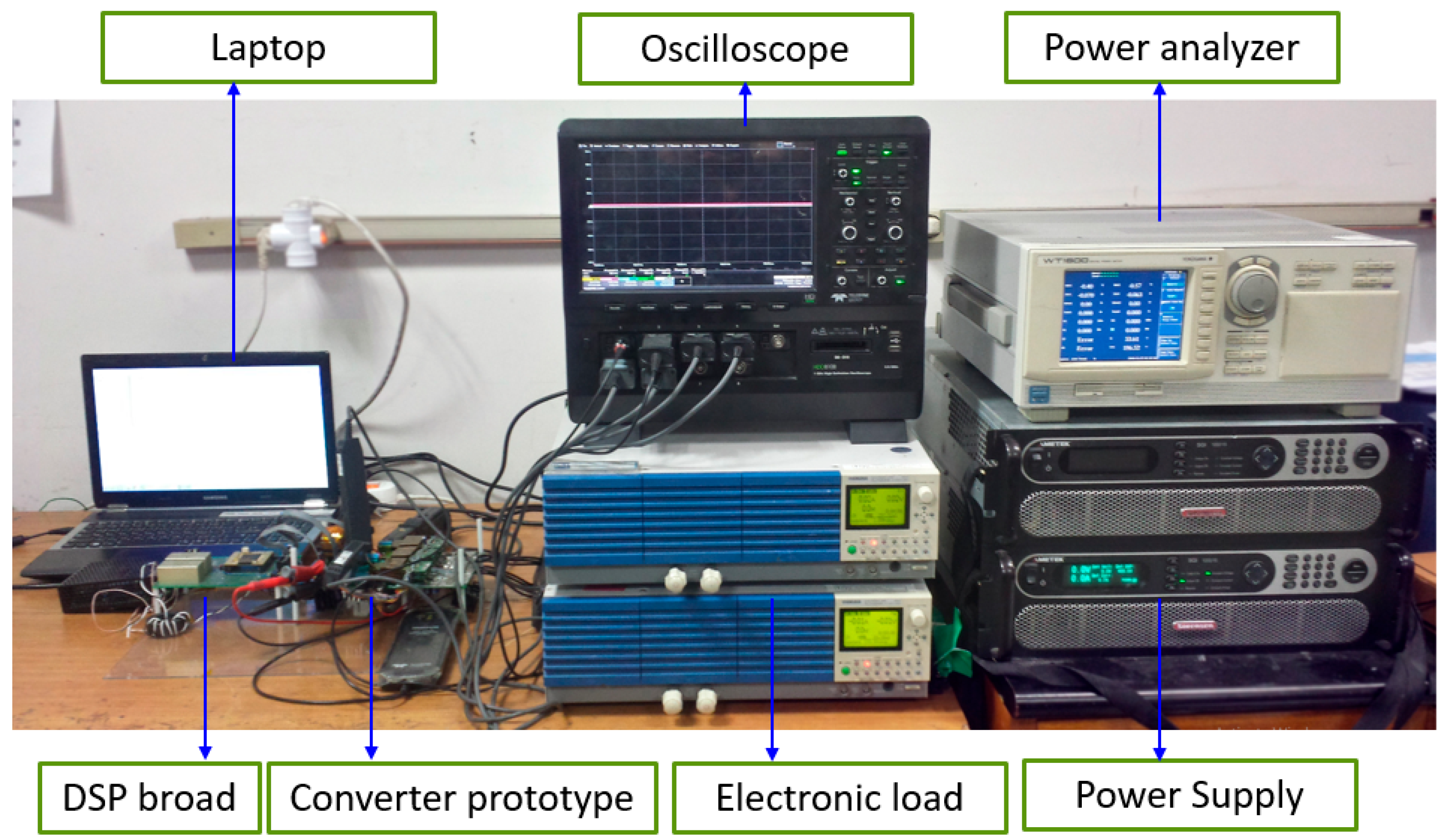
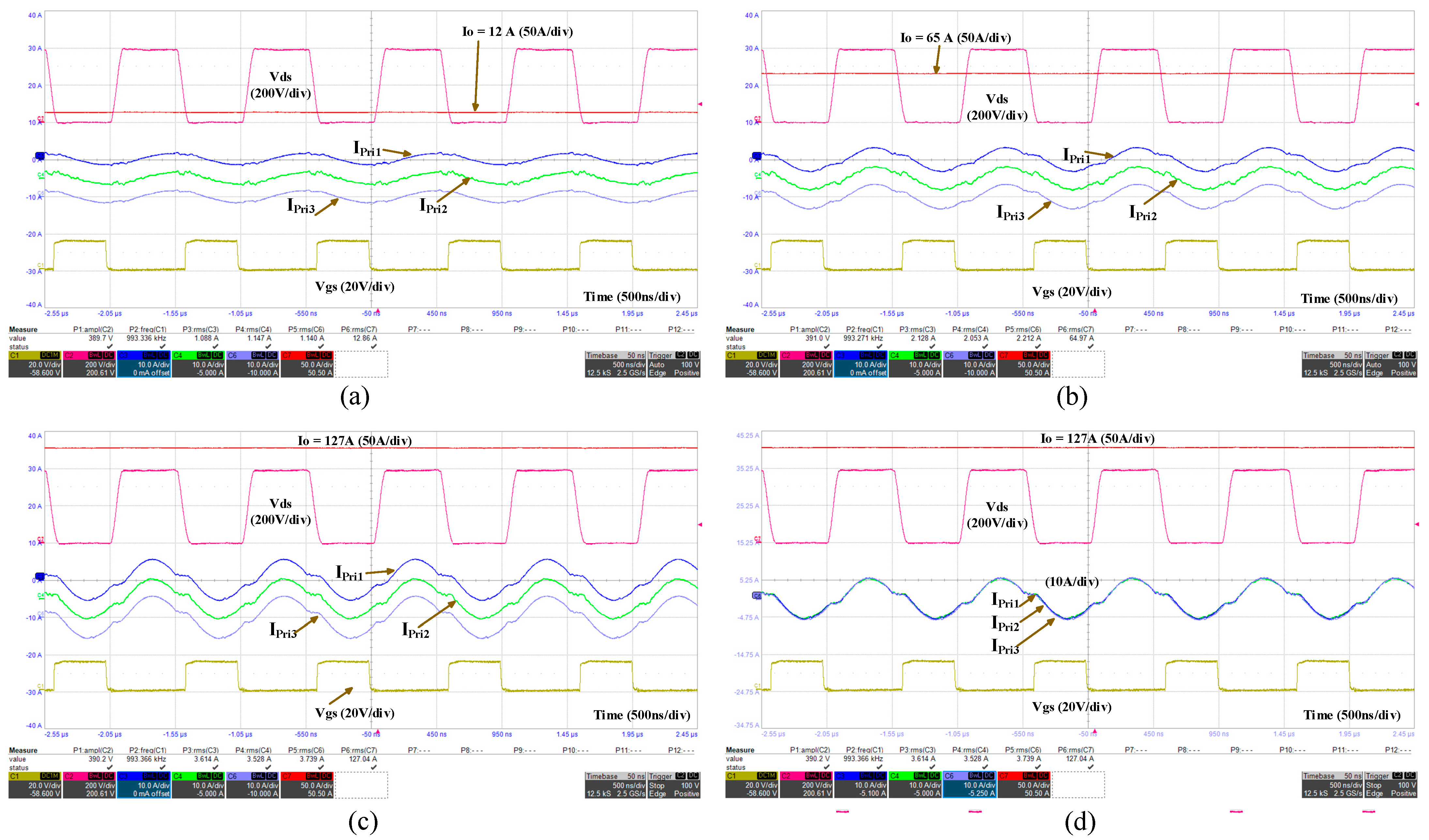
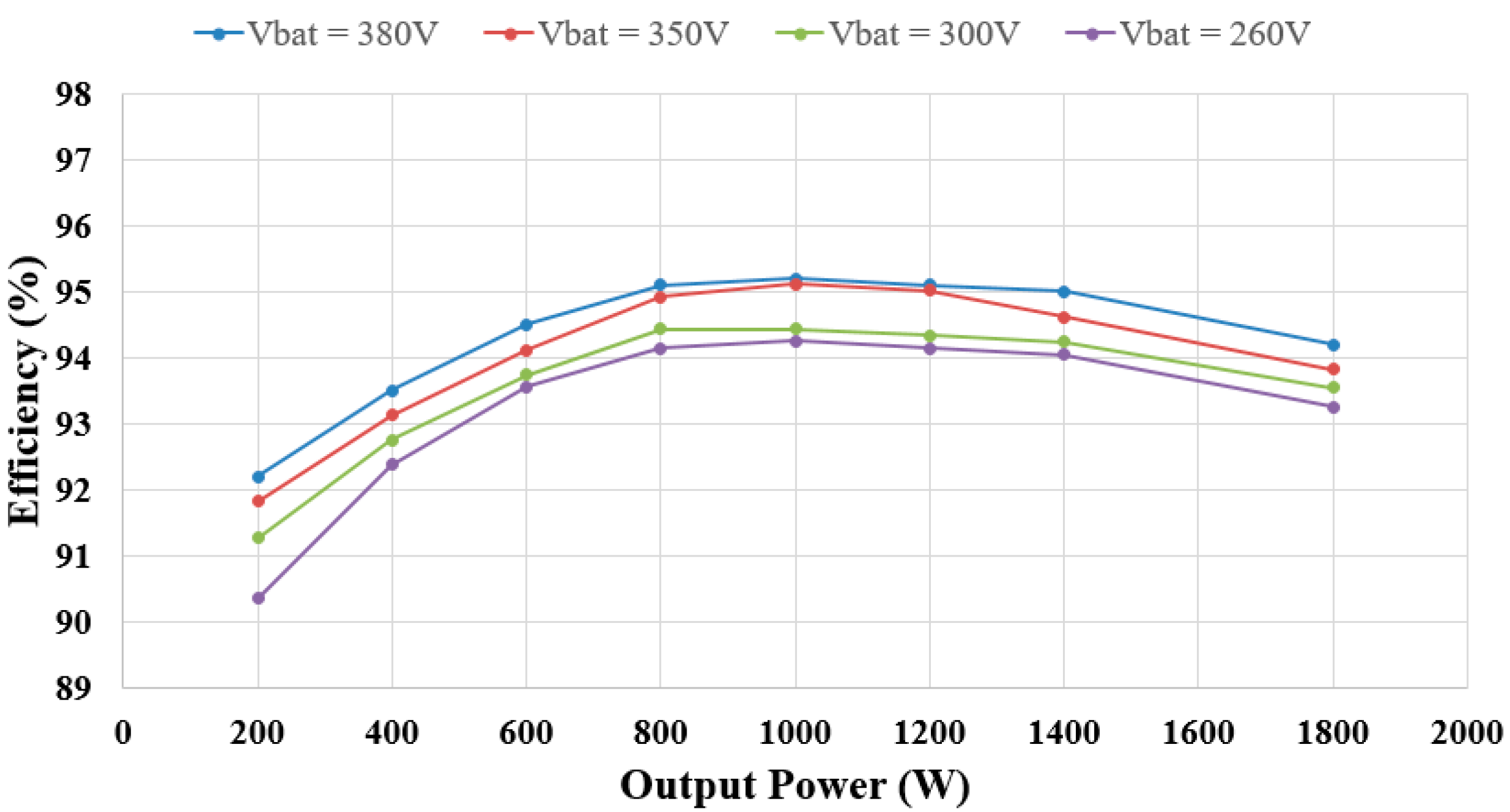
4. Experimental Results

In this section, a 1 MHz, 400 V/12 V, 1.8 kW prototype converter was developed to experimentally validate the performance of the proposed converter. The design incorporates a 600 W planar transformer, and its key parameters are summarized in Table 4.
By implementing the proposed interleaved transformer structure, a low leakage inductance of 1.4 µH was achieved and utilized as the series resonant inductance. The resonant capacitance was calculated using (16) to establish the resonant frequency at 1 MHz. L m was chosen so that (15) holds and ensures zero-voltage switching. As a result, a practical air gap of 25 µH was inserted between the two magnetic cores. It was found that k b is equal to 0.056 through the ratio of leakage inductance to magnetizing inductance. Experimentally, we found the actual voltage gain of the proposed converter and present it in Figure 10. The frequency of on-and-off use, or switching frequency, was kept at 1 MHz. We learned in the previous section that the voltage gain should stay level at the resonant frequency. Therefore, the variations in the output voltages among the parallel LLC converters are relatively insensitive to differences in the resonant elements.
Table 5 shows the main components of the LDC converter proposed in this study.
(1)
Cascode GaN HEMT has a much smaller Qg, which not only reduces the driving loss but also increases efficiency.
(2)
Achieving very low junction capacitance may incur higher cost, but it enables shorter deadtime or reduced magnetizing current to realize soft-switching ZVS both of which significantly improve converter efficiency at a 1 MHz operating frequency.
For IBB stage, silicon MOSFETs are selected and used at a 100 kHz switching frequency. At the LLC stage, GaN power transistors are designed in to ensure the device can switch quickly with maintained efficiency. We chose Transphorm’s TPH3206 cascode GaN HEMTs for the prototype in the lab due to their remarkable characteristics:
Careful consideration of special gate drivers and the complex design of the PCB is necessary for fast GaN operations. The Si8273 gate drivers from Silab are the best option to control high current primary switches. BSC010N27LSI was chosen due to its tiny R d s o n value, slim height, and tiny package, making it perfect to set directly on the secondary of the transformer. For this reason, the transformer is made using a commercial EE38/8/25 ferrite core with 3F4 core material due to its low magnetic power losses. Low ESR 1206-X7R 4.7 µF Multilayer Ceramic Capacitors are employed for absorbing the ripple voltage coming out of power supplies. A 3D software prototype for LDC application with 1.8 kW hardware power has been made which is 200 mm × 100 mm in size and contains an IBB stage combined with three parallel LLC stages, presented in Figure 11.
To evaluate the performance of the proposed LDC converter, the experimental hardware was set up as shown in Figure 12. The converter was supplied by 1000 V/15 A power supply. All waveforms were probed and displayed by TELEDYNE LECroy Oscilloscope. The efficiency was measured by a YOKOGAWA-WT1600 power analyzer. Two 1 kW-KiKusui PLZ1004W power electronic loads were connected in parallel to absorb 1.8 kW power and an external DSP TMS320F28335 board was used to control power converter board.
To validate the converter’s performance, three main waveforms were analyzed under load levels of 10%, 50%, and 100%, as shown in Figure 13. This diagram shows that V d s indicates the drain–source voltage on the low-side primary switch within a phase, and I o is the total current that comes out from the three parallel LLC stages. At resonance, the tank currents are IPri1, IPri2, and IPri3, and VGS is the signal driving the gate from the unpowered gate driver IC at the bottom. ZVS is maintained with primary-side switches across a wide variety of currents, including 12 A, 50 A, and 127 A, which is impressive at a high frequency of 1 MHz (Figure 13). Low levels of ringing on the drain-to-source voltage ( V D S ) show soft-switching is occurring as expected. Wiggles in dead time at low loads are caused by the engagement of transformer leakage inductance with the capacitance of the secondary rectifier switches.
The converter shares the current equally among all the switches in the complete range of loads, mainly due to its kb tuning and the use of a common resonant capacitor. As shown in Figure 13d, the difference between the resonant currents per phase does not exceed 5% at the full-load point of 1.8 kW.
The thermal images shown in Figure 14 further demonstrate power sharing among the individual phases of the LLC converter at both 20% and 100% load conditions.
The proposed converter is compared in Table 6 with other existing topologies to highlight that it has higher efficiency than any other topology with less complexity and simpler control mechanism. The proposed converter delivers 5.29 W/cm3, far above others at an estimated cost of USD 270.
When input voltage is higher (380 V), the IBB stage only processes a small differential power, allowing most power to flow directly through the more efficient LLC stages. The IBB stage has lower efficiency than the LLC stages. At lower input voltages, more power processing through the IBB stage leads to lower system efficiency overall.
Figure 15 illustrates the efficiency curves at different input voltage levels. The proposed converter reaches a peak efficiency of 95.2% at an output power of 1000 W with a battery voltage ( V bat ) of 380 V.

5. Conclusions

This paper has presented a novel LDC converter structure that integrates multiple advanced design strategies to achieve high power density and efficiency. The proposed topology is based on a cascoded two-stage structure, incorporating a low-parasitic planar transformer, Gallium Nitride (GaN) power transistors, and a passive current-sharing technique to address the challenges of high-frequency, high-power applications. A 1 MHz, 1.8 kW, 400 V/14 V LDC module intended for electric vehicle applications was successfully developed and tested. Comprehensive theoretical analysis, detailed operational principles, and experimental validation confirm the effectiveness of the proposed design. The results demonstrate that the converter achieves superior performance in terms of both efficiency and power density, making it a promising solution for next-generation electric vehicle power conversion systems.

Author Contributions

Conceptualization, T.M.T. and W.C.; Methodology, T.M.T.; Software, T.M.T.; Validation, T.M.T.; Formal analysis, A.S.A. and W.C.; Resources, W.C.; Writing—review & editing, A.S.A.; Visualization, A.S.A. and W.C.; Supervision, W.C. All authors have read and agreed to the published version of the manuscript.

Funding

This research received no external funding.

Data Availability Statement

The original contributions presented in this study are included in the article. Further inquiries can be directed to the corresponding author.

Conflicts of Interest

The authors declare no conflicts of interest.

References

  1. Rong, R.; Zeljkovic, S. A 2kW, 100kHz high speed IGBT based HV-LV DC/DC converter for electric vehicle. In Proceedings of the 2014 IEEE Conference and Expo Transportation Electrification Asia-Pacific (ITEC Asia-Pacific), Beijing, China, 31 August–3 September 2014. [Google Scholar]
  2. Hasan, S.M.N.; Anwar, M.N.; Teimorzadeh, M.; Tasky, D.P. Features and challenges for Auxiliary Power Module (APM) design for hybrid/electric vehicle applications. In Proceedings of the 2011 IEEE Vehicle Power and Propulsion Conference, Chicago, IL, USA, 6–9 September 2011; pp. 1–6. [Google Scholar] [CrossRef]
  3. Galek, M.; Mondal, G. Modular DC/DC converter with improved efficiency for electric vehicles applications. In Proceedings of the 2014 IEEE Applied Power Electronics Conference and Exposition—APEC 2014, Fort Worth, TX, USA, 16–20 March 2014; pp. 1958–1965. [Google Scholar]
  4. Tuan, T.M.; Choi, W. A novel two-stage power conversion method suitable for LDCs of the electric vehicles. In Proceedings of the 2019 10th International Conference on Power Electronics and ECCE Asia (ICPE 2019-ECCE Asia), Busan, Republic of Korea, 27–30 May 2019; pp. 1–7. [Google Scholar]
  5. Pang, Z.; Ren, X.; Xiang, J.; Chen, Q.; Ruan, X.; Chen, W. High-frequency DC-DC converter in electric vehicle based on GaN transistors. In Proceedings of the 2016 IEEE Energy Conversion Congress and Exposition (ECCE), Milwaukee, WI, USA, 18–22 September 2016; pp. 1–7. [Google Scholar] [CrossRef]
  6. Lu, B.; Liu, W.; Liang, Y.; Lee, F.C.; van Wyk, J.D. Optimal design methodology for LLC resonant converter. In Proceedings of the Twenty-First Annual IEEE Applied Power Electronics Conference and Exposition, 2006. APEC ‘06., Dallas, TX, USA, 19–23 March 2006. [Google Scholar]
  7. Fu, D.; Lu, B.; Lee, F.C. 1MHz High Efficiency LLC Resonant Converters with Synchronous Rectifier. In Proceedings of the 2007 IEEE Power Electronics Specialists Conference, Orlando, FL, USA, 17–21 June 2007; pp. 2404–2410. [Google Scholar]
  8. Wu, X.; Chen, H.; Qian, Z. 1-MHz LLC Resonant DC Transformer (DCX) With Regulating Capability. IEEE Trans. Ind. Electron. 2016, 63, 2904–2912. [Google Scholar] [CrossRef]
  9. Park, H.; Jung, J. PWM and PFM Hybrid Control Method for LLC Resonant Converters in High Switching Frequency Operation. IEEE Trans. Ind. Electron. 2017, 64, 253–263. [Google Scholar] [CrossRef]
  10. Fu, D.; Liu, Y.; Lee, F.C.; Xu, M. A novel driving scheme for synchronous rectifiers in LLC resonant converters. IEEE Trans. Power Electron. 2009, 24, 1321–1329. [Google Scholar] [CrossRef]
  11. Feng, W.; Lee, F.C.; Mattavelli, P.; Huang, D. A universal adaptive driving scheme for synchronous rectification in LLC resonant converters. IEEE Trans. Power Electron. 2012, 27, 3775–3781. [Google Scholar] [CrossRef]
  12. Kim, K.W.; Youn, H.S.; Baek, J.I.; Jeong, Y.; Moon, G.W. Analysis on Synchronous Rectifier Control to Improve Regulation Capability of High-Frequency LLC Resonant Converter. IEEE Trans. Power Electron. 2017, 33, 1–10. [Google Scholar] [CrossRef]
  13. Wang, H.; Chen, Y.; Qiu, Y.J.; Fang, P.; Zhang, Y.; Wang, L.L. Common Capacitor Multiphase LLC Converter With Passive Current Sharing Ability. IEEE Trans. Power Electron. 2018, 33, 370–387. [Google Scholar] [CrossRef]
  14. Hu, Z.; Qiu, Y.; Wang, L.; Liu, Y.-F. An interleaved LLC resonant converter operating at constant switching frequency. In Proceedings of the 2012 IEEE Energy Conversion Congress and Exposition (ECCE), Raleigh, NC, USA, 15–20 September 2012; pp. 3541–3548. [Google Scholar]
  15. Wu, H.; Zhan, X.; Xing, Y. Interleaved LLC resonant converter with hybrid rectifier and variable-frequency plus phase-shift control for wide output voltage range applications. IEEE Trans. Power Electron. 2017, 32, 4246–4257. [Google Scholar] [CrossRef]
  16. Figge, H.; Grote, T.; Froehleke, N.; Boecker, J.; Ide, P. Paralleling of LLC resonant converters using frequency controlled current balancing. In Proceedings of the 2008 IEEE Power Electronics Specialists Conference, Rhodes, Greece, 15–19 June 2008; pp. 1080–1085. [Google Scholar]
  17. Huang, X.; Liu, Z.; Li, Q.; Lee, F.C. Evaluation and Application of 600 V GaN HEMT in Cascode Structure. IEEE Trans. Power Electron. 2014, 29, 2453–2461. [Google Scholar] [CrossRef]
  18. Hariya, A.; Yanagi, H.; Ishizuka, Y.; Matsuura, K.; Tomioka, S.; Ninomiya, T. 5MHz PWM-controlled current-mode resonant DC–DC converter with GaN-FETs. In Proceedings of the 2014 IEEE Applied Power Electronics Conference and Exposition—APEC 2014, Fort Worth, TX, USA, 16–20 March 2014; pp. 1426–1432. [Google Scholar]
  19. Reusch, D.; Strydom, J. Evaluation of Gallium Nitride Transistors in High Frequency Resonant and Soft-Switching DC–DC Converters. IEEE Trans. Power Electron. 2015, 30, 5151–5158. [Google Scholar] [CrossRef]
  20. Zhang, W.; Wang, F.; Costinett, D.J.; Tolbert, L.M.; Blalock, B.J. Investigation of Gallium Nitride Devices in High-Frequency LLC Resonant Converters. IEEE Trans. Power Electron. 2017, 32, 571–583. [Google Scholar] [CrossRef]
  21. Lu, J.; Dawson, F. Characterizations of High Frequency Planar Transformer With a Novel Comb-Shaped Shield. IEEE Trans. Magn. 2011, 47, 4493–4496. [Google Scholar] [CrossRef]
  22. Ouyang, Z.; Thomsen, O.C.; Andersen, M.A.E. Optimal Design and Tradeoff Analysis of Planar Transformer in High-Power DC–DC Converters. IEEE Trans. Ind. Electron. 2012, 59, 2800–2810. [Google Scholar] [CrossRef]
  23. Pahlevaninezhad, M.; Hamza, D.; Jain, P.K. An Improved Layout Strategy for Common-Mode EMI Suppression Applicable to High-Frequency Planar Transformers in High-Power DC/DC Converters Used for Electric Vehicles. IEEE Trans. Power Electron. 2014, 29, 1211–1228. [Google Scholar] [CrossRef]
  24. Saket, M.A.; Shafiei, N.; Ordonez, M. LLC Converters With Planar Transformers: Issues and Mitigation. IEEE Trans. Power Electron. 2017, 32, 4524–4542. [Google Scholar] [CrossRef]
  25. Fu, D.; Lee, F.C.; Wang, S. Investigation on transformer design of high frequency high efficiency dc-dc converters. In Proceedings of the 2010 Twenty-Fifth Annual IEEE Applied Power Electronics Conference and Exposition (APEC), Palm Springs, CA, USA, 21–25 February 2010; pp. 940–947. [Google Scholar]
  26. Yan, C.; Li, F.; Zeng, J.; Liu, T.; Ying, J. A Novel Transformer Structure for High power, High Frequency converter. In Proceedings of the 2007 IEEE Power Electronics Specialists Conference, Orlando, FL, USA, 17–21 June 2007; pp. 214–218. [Google Scholar]
  27. Huang, D.; Ji, S.; Lee, F.C. LLC Resonant Converter With Matrix Transformer. IEEE Trans. Power Electron. 2014, 29, 4339–4347. [Google Scholar] [CrossRef]
  28. Mu, M.; Lee, F.C. Design and Optimization of a 380–12 V High-Frequency, High-Current LLC Converter With GaN Devices and Planar Matrix Transformers. IEEE J. Emerg. Sel. Top. Power Electron. 2016, 4, 854–862. [Google Scholar]
  29. Fei, C.; Lee, F.C.; Li, Q. High-Efficiency High-Power-Density LLC Converter With an Integrated Planar Matrix Transformer for High-Output Current Applications. IEEE Trans. Ind. Electron. 2017, 64, 9072–9082. [Google Scholar] [CrossRef]
  30. Singh, A.R.; Suresh, K.; Parimalasundar, E.; Kumer, B.H.; Bajaj, M.; Tuka, M.B. Design and performance evaluation of a multi-load and multi-source DC-DC converter for efficient electric vehicle power systems. Sci. Rep. 2024, 14, 25718. [Google Scholar] [CrossRef] [PubMed]
  31. Yang, G.; Dubus, P.; Sadarnac, D. Double-phase high-efficiency, wide load range high-voltage/low-voltage LLC DC/DC converter for electric/hybrid vehicles. IEEE Trans. Power Electron. 2015, 30, 1876–1886. [Google Scholar] [CrossRef]
  32. Guan, Q.; Rubino, L.; Wang, Z.; Bozhko, S. Design and implementation of GaN-based dual-active-bridge DC/DC converters. IEEE Trans. Ind. Electron. 2020, 67, 9982–9992. [Google Scholar]
Figure 1. Block diagram of HV/LV between vehicle batteries.
Electronics 14 02403 g001
Figure 2. (a) Complete architecture of proposed LDC topology; (b) simplified equivalent using a single LLC converter.
Electronics 14 02403 g002
Figure 3. Key waveforms of proposed converter at fSW = f0.
Electronics 14 02403 g003
Figure 4. Simplified equivalent model and its corresponding fundamental harmonic representation for LLC stage.
Electronics 14 02403 g004
Figure 5. (a) Cascoded two stage converter block diagram structure; (b) power flow illustration of proposed converter.
Electronics 14 02403 g005
Figure 6. Power flow distribution from battery and IBB to LLC stage.
Electronics 14 02403 g006
Figure 7. Phasor diagrams illustrating capacitor voltages and resonant currents Ipri1, Ipri2, and Ipri3: Without common capacitor technique (a) and with application of common capacitor technique (bd).
Electronics 14 02403 g007
Figure 8. Variation of voltage gain with switching frequency for multiple leakage-to-magnetizing inductance ratios kb = Lr/Lm.
Electronics 14 02403 g008
Figure 9. Cross view of transformer structure. (a) Interleaving–overlap primary winding structure; (b) interleaving–minimized-overlap winding structure.
Electronics 14 02403 g009
Figure 10. Voltage conversion gain profile of three parallel LLC converter in proposed LDC design.
Electronics 14 02403 g010
Figure 11. (a) 3D prototype designed by software; (b) real hardware of proposed converter.
Electronics 14 02403 g011
Figure 12. Photograph of hardware experimental setup.
Electronics 14 02403 g012
Figure 13. Three phase LLC stage waveforms of at (a) 10%, (b) 50%, (c) 100% load; (d) current sharing capacity at 100% load.
Electronics 14 02403 g013
Figure 14. Converter thermal images at 20% load and 100% load.
Electronics 14 02403 g014
Figure 15. Measured efficiency of proposed LDC converter.
Electronics 14 02403 g015
Table 1. Design specifications of LDC converters.
ParametersSymbolsValues
Maximum output power P o , m a x 1.8 [kW]
Input voltage V i n 260–400 [V]
Output voltage V o 14 [V]
Switching frequency f S w 1 [MHz]
Table 2. Design and operating parameters of IBB stage.
ParametersSymbolsValues
InductorL1350 [µH]
Output capacitorC1100 [µF]
Input voltageVin260–400 [V]
Output voltageVdc,min~Vdc,max0–140 [V]
Switching frequencyfsw_ibb100 [kHz]
Maximum output powerPIBB650 [W]
Table 3. Design specifications of single-phase LLC circuit.
ParametersSymbolsValues
Maximum power P O 600 [W]
Input voltage V i n 400 [V]
Output voltage V o 14 [V]
Switching frequency f S w 1 [MHz]
Turn ration16:1
Table 4. Electrical and structural characteristics of 600 W planar transformer.
ParametersSymbolsValues
Resonant capacitorCr 18   [ nF ]
Leakage inductanceLlk = Lr 1.4   [ μ H ]
Magnetizing inductanceLm 25   [ μ H ]
Core type EE38/8/25
Core material 3F4
PCB layer material FR-4
Insulator Kapton tape
Primary side copper width 1.2 mm
Primary side copper thickness 2 oz
Secondary side copper width 1.2 mm
Secondary side copper thickness 2 oz
Turn ration16:1:1
Table 5. Components list for prototype of proposed converter.
ComponentsManufacturersParts
IBB stage MOSFETs
IBB stage inductance core
IXYZIXFB110N60P3
Primary MOSFETsTransphormTPH3206 (GaN)
Primary gate drive ICSilabSi8273
Secondary rectifiersInfineonBSC010N27LSI
Magnetic ferrite core of TRFerroxcubeEE38/8/25-3F4
Resonant film capacitorsEPCOSB32912B3334M
Output capacitorsKEMET4.7 µF/MCLL
Table 6. Comparison between proposed and existing topologies.
ReferenceNumber of Components
(S, I, C, TF) *
Switching FrequencyVoltage GainEfficiencyControl ComplexityCurrent StressVoltage StressPower Density (W/cm3)Cost (USD)
Proposed14, 4, 5, 31 MHzEquation (3)95.2% peakMedium (fixed freq.) I s t r e s s = P o u t 3 η V i n 1 1 D 1 V s w = V i n   I B B V s w =   V i n   2 L L C 5.29270
[30]5, 2, 2, 010 kHzLower90–93%Simplified Δ I L 1 =   1 A v 1 V 1 D 11 L 1 V s w =   V a   1 D N/A100
[31]4, 2, 2, 1125 kHz–1 MHzMedium90–93%High (freq. modulation) I p k = π P o u t 2 V i n f s L m V s w = V i n   1200
[13]8, 1, 2, 170–100 kHzLimited range92–94%Medium (phase shift) I p k = V i n 4 f s L V s w = V i n   N/A100
[32]12, 3, 4, 3500 kHz–1 MHzLimited range93–95%Very High (Interleaving control) I p h a s e = P o u t η p h a s e η V i n V s w = V i n   2 N/A250
* Number of components (switches, inductors, capacitors, and transformers).
Disclaimer/Publisher’s Note: The statements, opinions and data contained in all publications are solely those of the individual author(s) and contributor(s) and not of MDPI and/or the editor(s). MDPI and/or the editor(s) disclaim responsibility for any injury to people or property resulting from any ideas, methods, instructions or products referred to in the content.

