Article

Ion-Induced Charge and Single-Event Burnout in Silicon Power UMOSFETs

by
Saulo G. Alberton
1,2,*,
Vitor A. P. Aguiar
1,
Nemitala Added
1,
Alexis C. Vilas-Bôas
3,
Marcilei A. Guazzelli
3,
Jeffery Wyss
4,5,
Luca Silvestrin
5,6,
Serena Mattiazzo
5,6,
Matheus S. Pereira
1,
Saulo Finco
7,
Alessandro Paccagnella
2 and
Nilberto H. Medina
1
1
Instituto de Física, Universidade de São Paulo, São Paulo 05508-090, Brazil
2
Dipartimento di Ingegneria Dell’Informazione, Università degli Studi di Padova, 35131 Padova, Italy
3
Centro Universitário FEI, São Bernardo do Campo 09850-901, Brazil
4
Dipartimento di Ingegneria Civile e Meccanica, Università degli Studi di Cassino e del Lazio Meridionale, 03043 Cassino, Italy
5
Istituto Nazionale di Fisica Nucleare–Sezione di Padova, 35131 Padova, Italy
6
Dipartimento di Fisica e Astronomia “Galileo Galilei”, Università degli Studi di Padova, 35131 Padova, Italy
7
Centro de Tecnologia da Informação Renato Archer, Campinas 13069-901, Brazil
*
Author to whom correspondence should be addressed.
Electronics 2025, 14(11), 2288; https://doi.org/10.3390/electronics14112288
Submission received: 18 April 2025 / Revised: 24 May 2025 / Accepted: 29 May 2025 / Published: 4 June 2025

Abstract

:
The U-shaped Metal-Oxide-Semiconductor Field-Effect Transistor (UMOS or trench FET) is one of the most widely used semiconductor power devices worldwide, increasingly replacing the traditional vertical double-diffused MOSFET (DMOSFET) in various applications due to its superior electrical performance. However, a detailed experimental comparison of ion-induced Single-Event Burnout (SEB) in similarly rated silicon (Si) UMOS and DMOS devices remains lacking. This study presents a comprehensive experimental comparison of ion-induced charge collection mechanisms and SEB susceptibility in similarly rated Si UMOS and DMOS devices. Charge collection mechanisms due to alpha particles from 241Am radiation source are analyzed, and SEB cross sections induced by heavy ions from particle accelerators are directly compared. The implications of the unique gate structure of Si UMOSFETs on their reliability in harsh radiation environments are discussed based on technology computer-aided design (TCAD) simulations.

1. Introduction

It is estimated that at least 50% of the global electricity consumption is controlled by power devices, which are primarily characterized by their ability to withstand high voltages [1]. When operating in radiation environments, power devices are susceptible to Single-Event Effects (SEEs) [2], which can disrupt their normal operation or even cause permanent damage. Due to their intense internal electric fields, power electronic devices are particularly susceptible to destructive SEEs [3]. Among the widely used power devices, Metal-Oxide-Semiconductor Field-Effect Transistors (MOSFETs) are predominant and are susceptible to Single-Event Burnout (SEB) destructive failure mode due to heavy ions [4], as present in an outer space environment, or neutrons [5], as present in a terrestrial atmospheric environment.
Figure 1 illustrates key MOSFET technologies relevant to this study. The vertical double-diffused MOSFET (DMOSFET) represents the most traditional technology in the power electronics industry, whereas the U-groove MOSFET (UMOSFET), also known as trench FET, is a more modern technology with notable advantages. For instance, UMOSFET fabrication processes enable significantly higher transistor cell densities on semiconductor wafers compared to DMOSFETs [6,7]. Additionally, UMOSFETs exhibit lower power dissipation than similarly rated DMOSFETs [7]. In recent years, DMOSFET technology has been gradually replaced by UMOSFET technology, establishing UMOSFETs as one of the most widely used semiconductor devices globally [7]. Although UMOSFETs generally exhibit superior electrical characteristics, their structural differences relative to DMOSFETs can lead to significantly different responses under radiation exposure. Therefore, it is essential to evaluate the reliability of UMOS technology and improve its radiation hardness before integrating it into high-reliability applications, such as space missions, terrestrial autonomous vehicles, and avionic systems operating at flight altitudes.
In the past decade, the absence of detailed experimental comparisons of SEB responses between similarly rated UMOS and DMOS devices has been emphasized in the literature [8]. An early computational study on heavy ion-induced SEB in a 70 V -rated silicon (Si) UMOSFET concluded that these devices are less sensitive to SEB than Si DMOSFETs [9]. However, this conclusion was not supported by experimental validation. Recent experimental research on atmospheric neutron-induced SEB in silicon-carbide (SiC)-based UMOS and DMOS power FETs concluded superior robustness of SiC UMOS architectures [10,11]. In contrast, a very recent systematic investigation of Si-based UMOS and DMOS devices demonstrated that Si UMOSFETs are more vulnerable to atmospheric neutron-induced SEB than their DMOSFET counterparts [5]. This apparent contradiction underscores fundamental differences in SEB mechanisms between Si and SiC technologies and highlights the need for a deeper investigation into charge collection dynamics in UMOSFET structures. Such understanding is essential for improving the reliability of next-generation UMOS devices.
In the context of space applications, this study investigates the SEE response of similarly rated Si-based N-type UMOS and DMOS power FETs under energetic ion irradiation. Charge collection mechanisms are analyzed by using alpha particles from a 241Am radiation source, whereas the SEB susceptibility of UMOS and DMOS devices is directly compared by using heavy ion beams provided by particle accelerators. Technology computer-aided design (TCAD) simulations are conducted to support analysis of experimental findings.

2. Materials and Methods

The SEEs induced by alpha particles and heavy ions were detected using techniques based on charge collection spectroscopy and transient current analysis, respectively.

2.1. Devices Under Test

Prior to electric characterization and irradiation, the encapsulation layers of the devices under test (DUTs) were removed through chemical etching, enabling the exposition of the device’s die area to impinging radiation. The DUTs were the IXFA220N06T3 UMOSFET and the IRLZ34NPbF DMOSFET parts, with rated drain-source breakdown voltages ( B V rated ) of 60 V and 55 V , respectively. Although their B V rated values differ slightly, these parts were specifically chosen for accurate comparisons of charge collection and SEE responses due to their nearly equivalent actual drain-source breakdown voltages ( B V DS ), as confirmed by precision measurements.
Figure 2 shows representative breakdown voltage curves, with both UMOS and DMOS devices exhibiting equivalent breakdown voltages of B V DS 70 V . The B V DS measurements were performed using high-precision SMUs (HP 41420A Source/Monitor Unit, 40 µ V 200 V / 20 fA 1 A ) connected to a high-performance modular system (HP 4142B Modular DC Source/Monitor) controlled by a computer. During these measurements, the DUTs were placed inside a Faraday cage to minimize electronic noise. They were configured in the non-negative gate off-state regime, with gate and source grounded ( V GS = 0 V ), while V DS was gradually increased until the drain-source leakage current ( I DSS ) reached a predefined limit. Following standard practice, the B V DS was defined as the condition where I DSS = 250 µ A at V DS = B V DS .

2.2. Alpha Particle Irradiation

The alpha particles were provided by a 241Am radioactive source, with a measured activity of 3.42 ( 10 ) × 10 5 particles . s 1 over a 4 π solid angle. The decapsulated DUTs were mounted under vacuum for frontal irradiation at room temperature, configured in the non-negative gate off-state ( V GS = 0 V and V DS 0 V ). Charge collection spectroscopy of SEEs induced by alpha particles was performed by using the acquisition system of the SAFIIRA facility [12], Brazil, which utilizes Nuclear Instrumentation Module (NIM) electronics. The system was calibrated with a high-precision charge signal generator (Ortec 419 Precision Pulse Generator). The charge collection spectra of the DUTs were recorded as a function of V DS . Since the UMOSFET and DMOSFET devices studied have similar breakdown voltages, this approach allows for a direct comparison of the main charge collection mechanisms between these FET technologies.

2.3. Heavy Ion Irradiation
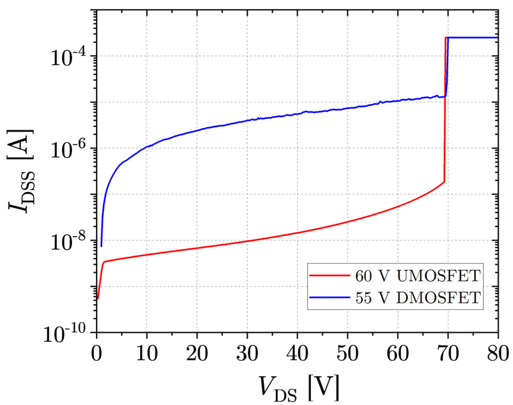
Since extensive studies on the ion-induced SEB response of the IRLZ34NPbF DMOSFET have already been published [4], the IXFA220N06T3 UMOSFET was irradiated with heavy ions in order to enable a direct comparison between SEB cross section measurements. Although a single MOSFET part was tested, SEB response is not expected to vary significantly among devices from the same production batch. The heavy ion irradiations were conducted in two campaigns using the 8 MV São Paulo Pelletron accelerator at the Laboratório Aberto de Física Nuclear (LAFN–USP), Brazil, and the 14 MV Tandem-XTU accelerator at the Istituto Nazionale di Fisica Nucleare—Laboratori Nazionali di Legnaro (INFN–LNL), Italy. The accelerators were used complementarily to cover a wide range of ion energies: low-energy experiments were performed at LAFN–USP using the SAFIIRA facility [12], and high-energy experiments were conducted at INFN–LNL using the SIRAD facility [13].
Figure 3 shows the schematic diagram of the experimental setup, which is based on the current-limiting technique [14], a standard non-destructive method for protective SEB measurements in power MOSFETs [15,16,17]. Using this setup, potential SEBs are detected and recorded as current pulse signals by an oscilloscope. At the LAFN–USP, a Rohde & Schwarz RTE 1104 oscilloscope ( 5 GSa / s , 1 GHz ) and a Cemipro ESHV 1500-010 power supply ( + 1500 V DC, 10.00 mA DC) were used. At the INFN–LNL, a LeCroy WaveRunner 640Zi oscilloscope ( 40 GSa / s , 4 GHz ) and a Keithley 248 power supply ( ± 5000 V DC, 5.000 mA DC) were utilized. In both setups, the input impedance of oscilloscopes were set to 50 Ω to avoid signal reflections, and an Agilent 355D VHF logarithmic attenuator ( 1 GHz , 50 Ω ) prevented them from overcurrent.
Heavy ion irradiation experiments were performed using 28 Si beams ( 50.2 to 120.0 MeV ) and 58 Ni beams ( 100.0 to 198.0 MeV ). Table 1 summarizes the characteristic parameters of the distinct ion beams used in this study. The particle fluence rates were maintained between 5 × 10 3 and 1 × 10 4 ions . s 1 . cm 2 , adjusted for each test run to avoid dead time losses. Frontal irradiation was performed at room temperature under high vacuum 10 5 Torr , with devices biased at V GS = 0 V and V DS > 0 V . For each V DS , irradiation continued until the typical beam fluence of Φ = 10 6 ions . cm 2 was reached [15,17]. The SEB cross section was calculated as the number of recorded SEB signals per unit fluence. This procedure was repeated at progressively higher V DS values, covering all ion-energy combinations.

3. Results

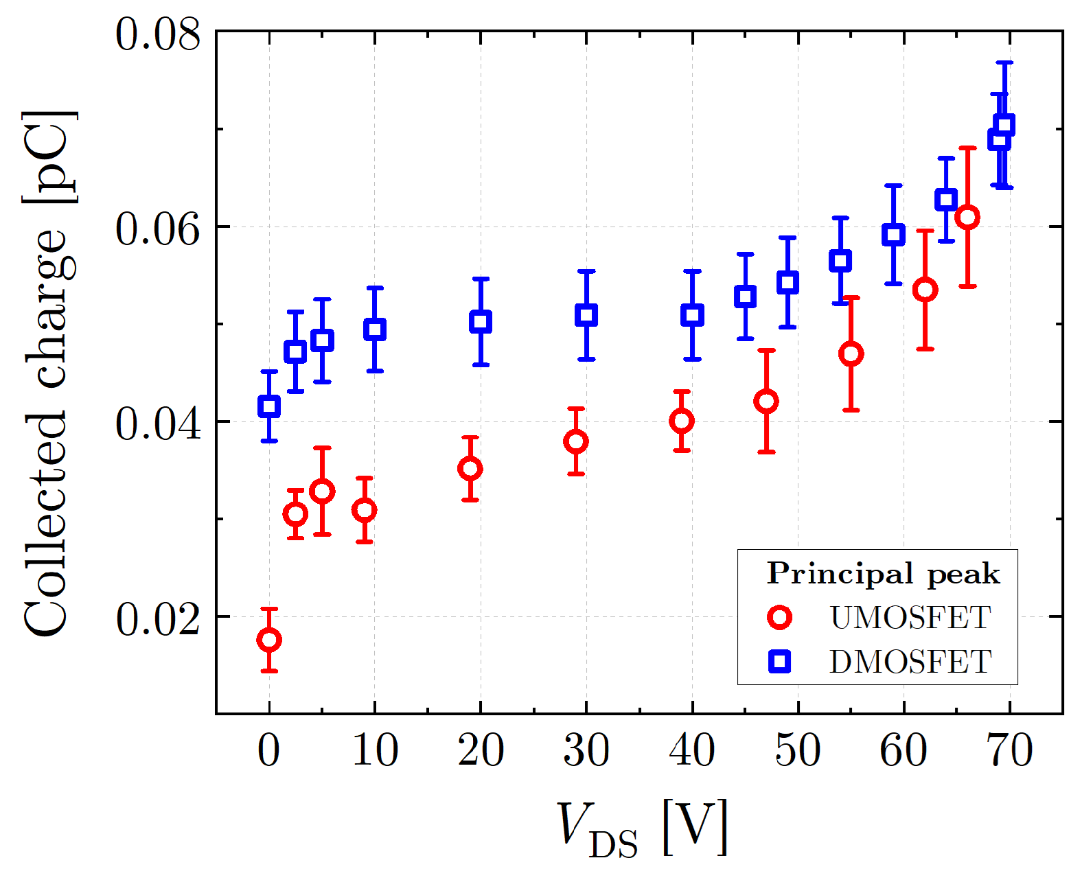
3.1. Alpha Particle Irradiation

Only non-destructive SEEs of the Single-Event Transient (SET) type were detected during alpha particle irradiation experiments in similarly rated DMOS and UMOS transistors with B V DS 70 V .
Figure 4 exhibits their charge collection spectra at different V DS levels. The charge collection spectra induced by alpha particles in the DUTs can be categorized into three main components: (i) a low-charge collection tail, (ii) a principal collection peak, and (iii) a high-charge collection tail. The dependence of the principal charge collection peaks on V DS is shown in Figure 5.
Regarding the charge collection mechanisms in the DMOSFET, it is first noted that the low-charge collection tail remains nearly independent on V DS . A previous study has reported detailed temporal analysis of ion-induced charge spectroscopy in a P-channel MOSFET, identifying similar low-collection tail and principal peak as due to diffusion and drift/funneling mechanisms, respectively [18]. These facts confirm that the observed low-charge collection tail results from a diffusion mechanism, where charge carriers are generated by the impinging ions in field-free regions of the device. In the absence of electric field, these carriers diffuse into the sensitive volume of the DMOSFET, where they are partially collected, thereby triggering a SEE. For instance, this scenario corresponds to ions impinging over the gate pad region, as denoted by (i) in Figure 6a. By contrast, the principal peak shifts forward as the applied V DS increases. As shown in Figure 5, the asymptotic dependence of collected charge on V DS at low voltages suggests depletion-region modulation, consistent with the interpretation of prompt charge collection [18]. Thus, the principal peaks in Figure 4 are attributed to ion impacts on the P-body/N-drift depletion region beneath the source contact, resulting in a diode current response (mechanism (ii) in Figure 6a). The high-charge collection tail, however, arises from ion impacts near the PN junction edges beneath the gate contact (mechanism (iii) in Figure 6a), where the electric fields are stronger than in parallel junctions [1]. The shape of the high-charge collection component is found to be even more dependent on V DS than the prompt collection peak. Ions impinging in this region may ultimately result in a parasitic BJT response [19,20].
Similarly to that observed in the DMOSFET, the low-collection tail in the UMOSFET is attributed to diffusion transport due to particle impact over field-free regions, such as the gate pad (mechanism (i) in Figure 6b). The UMOS response also exhibits a (ii) prompt collection peak and (iii) high-charge collection tail. As shown in Figure 4, at lower voltages, the charge collection in the UMOSFET resembles a Gaussian curve with slight positive skewness. However, as V DS increases, the high-energy tail becomes prominent. Notably, SEEs associated with high collected charge values are observed at high voltages, indicating that the influence of V D S on high-charge SEEs is even more pronounced in the UMOSFET than in the DMOSFET. Relatively high electric fields occur near the trench corners in the UMOSFET structure [1]. Therefore, the impact ionization process, which is highly dependent on the electric field intensity, is likely responsible for charge carrier multiplication in UMOSFETs operating at higher voltages (mechanism (iii) in Figure 6b).
Figure 5 shows the dependence of the principal charge collection peak on V DS . As previously noted, charge collection approximately follows a V DS dependence at lower voltages ( V DS < 50 V ), apart from a constant offset, due to depletion-region modulation. In this regime, the DMOSFET exhibits superior collection efficiency, which likely arises from its usually deep P-body/plug extension, as illustrated in Figure 6a. At higher voltages ( V DS > 50 V ), the prompt collected charge exhibits exponential growth. This behavior provides clear evidence that impact ionization plays a significant role in the charge multiplication mechanism of the high-collection tail, as the data reflect the exponential dependence of impact ionization on electric field intensity [21]. Figure 4 reveals that impact ionization is more pronounced in the UMOSFET, evidenced by its maximum collected charge surpassing that of the DMOSFET at higher voltages. Additionally, Figure 5 shows that the average prompt collected charge increases more rapidly in the UMOSFET as V DS increases, further supporting the conclusion that internal electric field favors charge multiplication through impact ionization.
Table 2 presents the non-destructive SEE cross section ( σ SEE ) for irradiated power transistors. The UMOSFET exhibits a higher absolute SEE cross section than the DMOSFET, indicating a higher susceptibility to alpha particle-induced SEEs. Power transistors typically consist of multiple parallel identical transistor cells, with UMOSFETs achieving significantly higher cell densities than DMOSFETs [6,7]. This structural difference explains the increased SEE sensitivity of the UMOSFET, which arises from both a higher transistor cell density and a larger total die area. In order to evaluate the intrinsic SEE vulnerability of each technology independently of die area dimensions, it is convenient to normalize the σ SEE by die area. The normalized results, also presented in Table 2, reveal that both technologies exhibit comparable SEE susceptibility per unit area, with approximately 50% of the irradiated device areas being sensitive to SEEs induced by alpha particles.
Although alpha particle irradiation results provide limited insight into overall device reliability, experimental data confirm significant charge multiplication due to impact ionization in UMOSFETs operating at high bias voltages. Contrary to early computational prediction [9], this enhanced charge multiplication suggests UMOSFETs may be more prone to destructive radiation effects like SEBs, which critically depend on impact ionization. To validate this hypothesis, heavy ion irradiation experiments are required for a comprehensive SEB reliability comparison between UMOS and DMOS technologies.

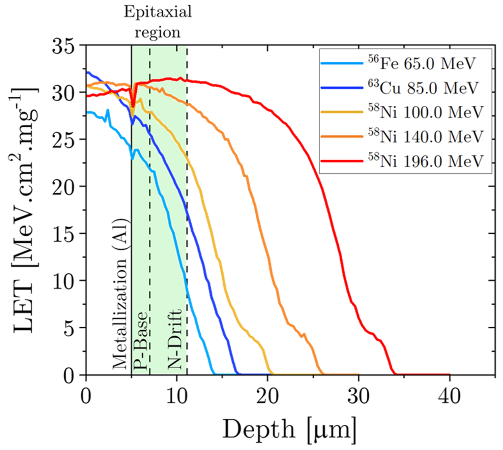
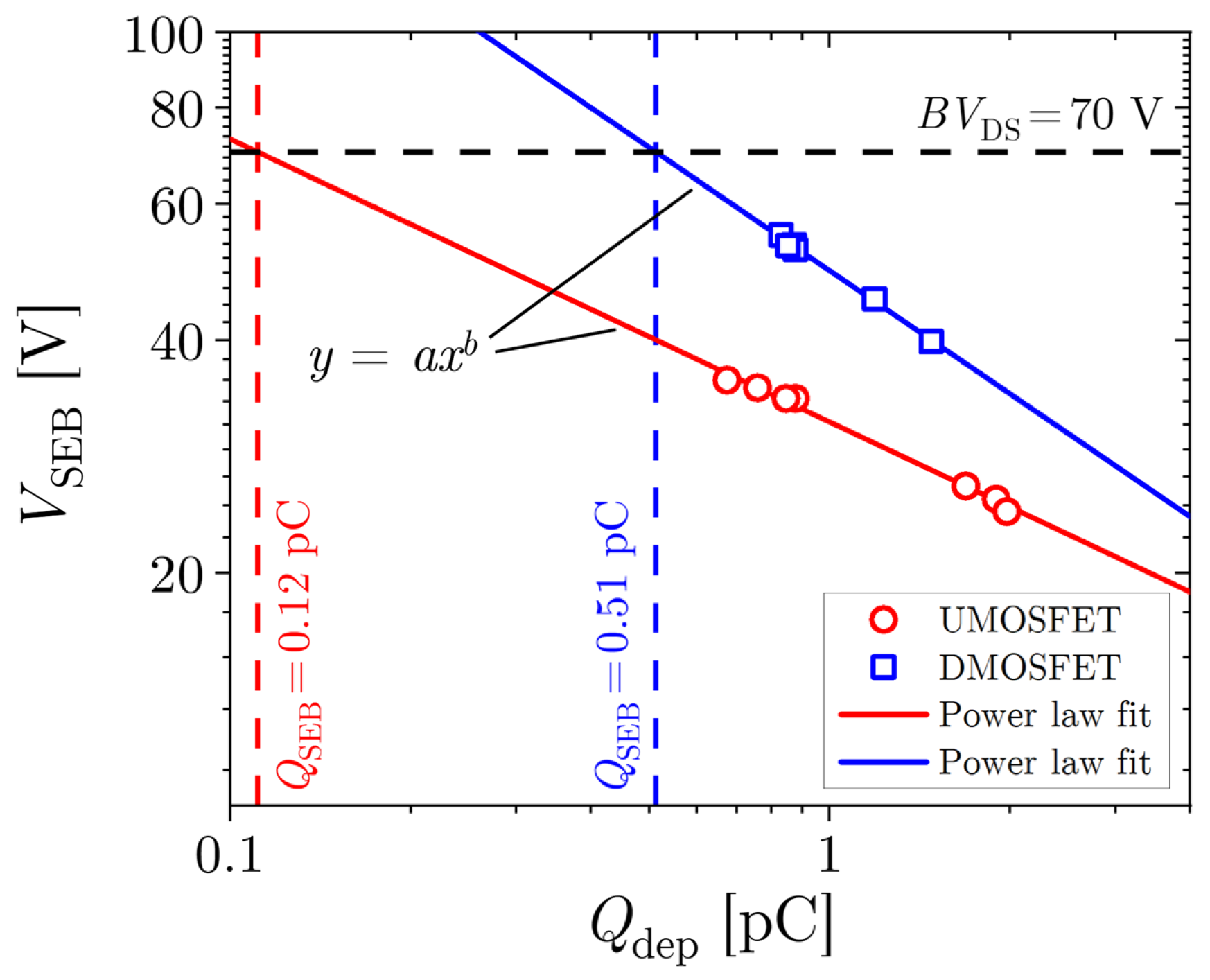
3.2. Heavy Ion Irradiation

Heavy ion-induced SEB cross sections in the IRLZ34NPbF DMOSFET from previous studies [4] were compared with SEB measurements in the IXFA220N06T3 UMOSFET. Both devices have actual breakdown voltages of approximately 70 V . No significant ion-induced microdose effects [22] were observed in the UMOSFET during irradiation runs, where the measured I DSS of the UMOSFET remained below 1 µ A , consistent with its maximum characteristic value of 10 µA, according to the device datasheet [23]. Unlike the UMOSFETs investigated in [22], the IXFA220N06T3 UMOSFET is not particularly designed in a stripe geometry. In order to enable direct comparison between devices with different die areas, the measured σ SEB were normalized by the die area of each DUTs, enabling a more accurate reliability analysis.
Figure 7 shows the dependence of heavy ion-induced SEBs on V DS for similarly rated DMOS and UMOS devices under 28Si irradiation. Although the irradiation energy values differ between devices, their energy ranges overlap within the 50–70 MeV interval ensures valid comparative analysis. Despite having equivalent breakdown voltages, the UMOS device triggers SEBs at significantly lower operating voltages than the DMOS device across the studied energy range. By fitting cumulative Weibull distributions to the experimental data [24], we determined statistical SEB threshold voltages. Whereas the DMOSFET exhibits SEBs at voltage ratios V DS / B V DS 75 %, SEBs can be triggered in the UMOS transistor at ratios as low as V DS / B V DS 50 %. Based on results from alpha particle irradiation presented in Section 3.1, the heavy ion data presented in Figure 7 indicate that enhanced charge multiplication through impact ionization in UMOSFETs is likely the primary cause of their higher SEB vulnerability compared to DMOSFETs.
It should be mentioned that the protective circuitry ( R p = 33 k Ω ) failed to prevent SEBs induced by 50.2 MeV 28Si ions in the UMOSFET, ultimately resulting in device destruction (drain-source short-circuit). In order to contextualize this result, we applied the model of Titus and Wheatley for worst-case SEE prediction [25]. For a fully depleted Si-based vertical MOSFET ( V DS = B V DS = 70 V ) without a buffer layer, the model predicts critical irradiation conditions for 28Si ( Z = 14 ) at 68 MeV . For the energy range considered in our experiments, the data shown in Figure 7 confirm that the critical energy for 28Si impinging the UMOSFET lies between 50.2 MeV and 72.0 MeV , consistent with model prediction. For the DMOSFET under a fully depleted condition, the prediction of the Titus–Wheatley model ( 68 MeV ) aligns with experimental worst-case ( 58.9 MeV ) within approximately 15% variation.
Figure 8 presents additional SEB cross section measurements for the IRLZ34NPbF DMOSFET and the IXFA220N06T3 UMOSFET due to distinct ion species with atomic numbers ranging from Z = 26 to Z = 29 . These ion species include 56Fe ( Z = 26 ), 58Ni ( Z = 28 ), and 63Cu ( Z = 29 ) at distinct energies. The DMOSFET data are sourced from prior studies [4], whereas the UMOSFET data are from original experimental measurements. Complementing the 28Si ( Z = 14 ) irradiation results shown in Figure 7, the data in Figure 8 further confirm the higher susceptibility of the UMOSFET to SEB compared to the similarly rated DMOSFET under heavy ion irradiation in the Z = 26–29 range. The SEB response of both transistors can be qualitatively explained by examining energy deposition in their epitaxial regions. Figure 9 shows the Linear Energy Transfer (LET) curves of the heavy ions from Figure 8 impinging on a fully depleted 70 V generic MOSFET structure, simulated by using the SRIM code [26]. For simplicity, the simulated generic MOSFET structure consists of a 5 µ m -thick aluminum metallization layer, a 2 µ m -thick P-base layer, and a 4.1 µ m -thick N-drift layer. As shown in Figure 9, the energy deposition within the epitaxial region increases progressively from 65.0 MeV 56Fe to 196.0 MeV 58Ni irradiation. This trend aligns with the observed variation in SEB threshold voltages ( V SEB ) in Figure 8, where higher energy deposition correlates with lower V SEB . The relationship between V SEB and the deposited charge in the epitaxial region ( Q dep ) can be estimated for both devices using LET curves simulated with SRIM for the ion-energy combinations presented in Figure 7 and Figure 8. This analysis reinforces the superior SEB susceptibility of the UMOS device based solely on deposited charge, regardless of the ion-energy combination adopted.
Figure 10 presents the dependence of V SEB on Q dep for both UMOS and DMOS devices. Across the investigated Q dep range, the UMOSFET consistently exhibits significantly lower SEB threshold voltages compared to the DMOSFET. These results complement the earlier demonstration in Figure 7, which demonstrated the greater vulnerability of the UMOSFET under identical ion species. The experimental data include several ion species at various energies. The relationship between V SEB and Q dep for both device types can be approximated by a power-law model of the form y = a x b . Table 3 presents the power law curve fit parameters a and b for UMOS and DMOS data. From this model, one estimates the minimum deposited charge within the epitaxial region required to induce SEB ( Q SEB ) to be 0.12 pC for the UMOSFET and 0.51 pC for the DMOSFET. These results demonstrate that a UMOSFET with B V DS = 70 V not only exhibits the lower SEB threshold voltages but also requires less deposited charge to initiate SEBs, approximately 20% of the critical charge needed for a DMOSFET counterpart. This simple model can explain why alpha particles from a 241Am source cannot induce SEB in the DUTs. SRIM simulations reveal that 5.486 MeV alpha particles deposit a maximum of 0.043 pC in the fully depleted epitaxial region of a 70 V generic MOSFET structure, which remains below the Q SEB thresholds for both device types. The combination of reduced V SEB and lower Q SEB thresholds makes current UMOSFET designs more susceptible to heavy ion-induced SEB compared to similarly rated DMOSFETs.

4. Discussion

Two-dimensional TCAD simulations were performed using ECORCE software (v 2.26) [27] on a generic UMOSFET with B V DS = 70 V to analyze the SEB dynamics in this device and corroborate experimental observations induced by heavy ions. Although detailed design and process parameters for the IXFA220N06T3 UMOSFET are unavailable, the simulated UMOS structure was engineered to replicate its key electrical characteristics. The implications of potential parameter variations were not considered in this study. For instance, the simulated devices achieves a breakdown voltage of B V DS = 70 V , consistent with measurements in Figure 2, and a threshold voltage of V th = 3.1 V , which is acceptable as a typical value according the datasheet ( V th = 2.0–4.0) [23]. The blocking and transfer characteristics of the simulated UMOSFET are presented in Figure 11.
The simulated structure comprises a N-drift region with a doping concentration of 4.5 × 10 15 cm 3 and a thickness of 5.1 µ m below the P-base/N-drift junction. The N-source region features a doping concentration of 1.0 × 10 19 cm 3 and a depth of 0.5 µ m , whereas the P-base region was assumed with a doping concentration of 1.0 × 10 17 cm 3 and a depth of 1.5 µ m . The gate oxide was modeled with a thickness of 50 nm along the trench sidewalls and 0.5 µ m -thick at the bottom surface. A half-cell with a width of 1.5 µ m was adopted as a representative unit cell [6]. The adopted physics models incorporate carrier generation by impact ionization and band-to-band tunneling, recombination via Shockley–Read–Hall and Auger processes, radiation-induced electron-hole pair separation (through a yield function), band-gap narrowing, and carrier mobility dependent on electric field and doping concentration [27].
Figure 12 presents a visualization of the simulated doping profiles, device geometry, and the peak electric field distributions following a 50 MeV 28Si strike at x = 0.75 µ m , as marked by the dashed green line. This ion energy represents one of the most severe irradiation conditions observed experimentally in the UMOSFET under 28 Si exposure, as previously shown in Figure 7. Under high-bias conditions ( V DS = 55 V ), the electric field peak shifts toward the drift/substrate junction due to the Egawa effect [28], surpassing the critical electric field of silicon ( E crit 0.3 MV . cm 1 [29]) and triggering a SEB. However, in alignment with experimental results, SEB does not occur at sufficiently lower bias voltages, such as V DS = 25 V . Recent TCAD simulations of ion-induced SEB in 150 V-rated UMOS and DMOS devices revealed significantly higher peak electric field intensities in the UMOS structure compared to the DMOS counterpart with equivalent voltage ratings [5].
Figure 13 shows peak electric field distributions resulting from a 50 MeV 28Si striking the trench gate column at x = 1.20 µ m , as marked by the dashed green line. The SEB response resembles that obtained for ion strikes over the N-source region. However, while the field in the drift/substrate junction reaches the silicon critical field, intense electric fields also develop in the vicinity of trench gate structure. Figure 13 exhibits the field distributions along the ion impact position (position A, dashed green line, x = 1.20 µ m ) and the vicinity of trench sidewalls in silicon (position B, dashed blue line, x = 0.99 µ m ). Along the ion strike position (position A), the electric field in the gate dielectric exceeds that in the semiconductor material due to distinct relative permittivities for SiO2 ( ε r = 3.9 ) and Si ( ε r = 11.9 ) [30]. Comparatively, the dielectric strength of SiO2 is approximately 10 MV . cm 1 [30]. After the ion strike, as the gate oxide is unshielded from the drain potential, it experiences rapid increase in electric field intensity, especially at high voltages. For ions with sufficiently high LETs and depending on the device gate oxide thickness, the resulting electric field spikes can ultimately induce the gate oxide rupture, also referred to as Single-Event Gate Rupture (SEGR) [31]. The ion impact further amplifies the electric field near the trench sidewall in silicon (position B), with the local field exceeding 0.3 MV . cm 1 at the trench corner. The peak field intensity at this location surpasses that observed for strikes at x = 0.75 µ m . These elevated fields promote carrier multiplication in silicon via impact ionization, as experimentally confirmed in Section 3.1. Although not experimentally observed in this study, elevated electric fields in the vicinity of channel regions can also promote hot-carrier injection into the gate oxide [6], generating oxide charge accumulation and the formation of interface traps. Over prolonged radiation exposure, these effects may lead to enhanced threshold voltage shifts and transconductance degradation [30].
Although trenches gates enable superior electrical performance of Si UMOSFETs, such as their notably low specific on-resistance, they simultaneously introduce reliability challenges with respect to radiation effects. Under energetic ion exposure, e.g., in space environments, intense electric fields are generated near the trench gate corners, potentially compromising the physical integrity of both the semiconductor and insulating materials. The results presented in this study are consistent with recent findings on atmospheric neutron effects in similarly rated Si UMOS and DMOS devices, which revealed an enhanced vulnerability of Si UMOSFETs to SEBs induced by secondary particles from nuclear reactions involving quasi-atmospheric neutrons and device materials [5]. Similarly to radiation-hardened Si DMOSFETs [32], a common hardening trend in UMOSFETs has been the incorporation of a buffer layer to reduce field concentrations at the drift-substrate junction following a particle strike [5,33]. Based on the findings of our present study, alternative strategies to further reduce electric field intensities at trench gate corners, along with the optimization of buffer layer design, may significantly improve the SEB tolerance of next-generation power UMOSFETs.
Based on computational studies in DMOSFETs [32], it is likely that incorporating buffer layers with optimized doping profiles and thicknesses, along with source (emitter) doping optimization, could enhance SEB robustness in UMOSFETs. A recent study suggest that this approach may also mitigate neutron-induced SEBs in UMOSFETs [5]. However, a detailed evaluation of UMOSFET structural optimization requires dedicated TCAD simulations studies, which falls beyond the scope of our current work.
Finally, consistent with our results using energetic ions, recent studies with monoenergetic neutrons [34] and quasi-atmospheric neutrons [5] confirm that Si-based UMOSFETs are generally more susceptible to premature charge multiplication and destructive radiation effects compared to similarly-rated DMOSFETs. However, as mentioned in the introduction, experimental research on atmospheric neutron-induced SEB in SiC-based UMOS and DMOS power FETs demonstrated superior robustness in SiC UMOS architectures [10,11]. This discrepancy between our observed vulnerability in Si UMOSFETs and the reported robustness of SiC UMOSFETs strongly supports the conclusion that SEB mechanisms differ fundamentally between Si and SiC MOSFETs. In fact, unlike the well-established SEB mechanism in Si MOSFETs [19,20], recent work suggests that SEB onset in SiC power MOSFETs may instead be governed by critical energy stored in the depletion region [35].

5. Conclusions

The ion-induced SEE response of similarly rated Si-based UMOS and DMOS power FETs was experimentally investigated under both alpha particle and heavy ion irradiation. The main aspects of their charge collection mechanisms and susceptibility to ion-induced SEB were comparatively analyzed. By using alpha particles from a 241Am radiation source, it was experimentally demonstrated that charge carrier multiplication is more pronounced in a UMOSFET than its DMOSFET counterpart during high-voltage operation. Contrary to earlier computational prediction and recent experiments involving SiC-based UMOS and DMOS transistors, heavy ion beam experiments with particle accelerators demonstrate that the Si-based UMOSFET generally initiates SEB at significantly lower thresholds and is substantially more vulnerable to heavy ion-induced SEB than its DMOSFET counterpart. These quantitative comparisons align with recent findings showing that similarly rated Si UMOSFETs are more vulnerable to premature multiplication effects induced by monoenergetic neutrons and SEBs induced by quasi-atmospheric neutrons. Since SEB in Si devices is strongly dependent on impact ionization and avalanche multiplication, the results confirm that carrier multiplication directly affects the radiation hardness of Si-based UMOSFETs in harsh environments. TCAD simulations attribute the increased SEB sensitivity of UMOSFETs to intense electric fields near the trench gate corners, which enhance the impact ionization process. Exploring new approaches to mitigate electric field concentrations at trench gate corners, combined with optimized buffer layer design, may substantially improve the SEB robustness of future Si-based UMOSFET devices. Our experimental data reveal a clear SEB vulnerability in Si UMOSFETs that contrasts with the documented SEB robustness of SiC UMOSFETs when both are compared to their DMOSFET counterparts. Consequently, this significant divergence provides strong evidence for fundamentally distinct SEB mechanisms between Si- and SiC-based power devices, as a recent study suggests.

Author Contributions

Conceptualization, S.G.A.; experimental methodology, validation, and measurement, S.G.A., V.A.P.A., N.A., A.C.V.-B., M.A.G., J.W., L.S., S.M. and N.H.M.; computational methodology and validation, S.G.A., V.A.P.A. and M.S.P.; investigation, S.G.A., V.A.P.A., N.A., M.S.P., A.C.V.-B., M.A.G., J.W., L.S., S.M., S.F., A.P. and N.H.M.; formal analysis, S.G.A.; resources, S.M., J.W., S.F., A.P. and N.H.M.; data curation, S.G.A.; writing—original draft preparation, S.G.A.; writing—review and editing, S.G.A., V.A.P.A., N.A., A.C.V.-B. and N.H.M.; supervision, N.H.M. and A.P.; funding acquisition, N.A., M.A.G., S.M., J.W., S.F., A.P. and N.H.M. All authors have read and agreed to the published version of the manuscript.

Funding

This study was financed in part by the Coordenação de Aperfeiçoamento de Pessoal de Nível Superior–Brasil (CAPES)–Financial Code 001; Conselho Nacional de Desenvolvimento Científico e Tecnológico (CNPq), Nos. 404054/2023-4 and 422360/2023-6; Fundação de Amparo à Pesquisa do Estado de São Paulo (FAPESP), No. 2023/16053-8; Financiadora de Estudos e Projetos (FINEP), No. 01.12.0224.00; Instituto Nacional de Ciência e Tecnologia: Física Nuclear e Aplicações (INCT-FNA), No. 464898/2014-5.

Data Availability Statement

The original contributions presented in this study are included in the article. Further inquiries may be directed to the corresponding author.

Acknowledgments

We sincerely acknowledge the technical staff of the Universidade de São Paulo, the Università degli Studi di Padova, the Istituto Nazionale di Fisica Nucleare—Laboratori Nazionali di Legnaro, and the Istituto Nazionale di Fisica Nucleare—Sezione di Padova for their valuable support. We especially wish to recognize exceptional contributions of Devis Pantano and Mario Tessaro.

Conflicts of Interest

The authors declare no conflicts of interest.

References

  1. Baliga, B.J. Fundamentals of Power Semiconductor Devices, 2nd ed.; Springer International Publishing AG: Cham, Switzerland, 2018. [Google Scholar]
  2. Aguiar, V.A.; Alberton, S.G.; Pereira, M.S. Radiation-Induced Effects on Semiconductor Devices: A Brief Review on Single-Event Effects, Their Dynamics, and Reliability Impacts. Chips 2025, 4, 12. [Google Scholar] [CrossRef]
  3. Sexton, F.W. Destructive single-event effects in semiconductor devices and ICs. IEEE Trans. Nucl. Sci. 2003, 50, 603–621. [Google Scholar] [CrossRef]
  4. Alberton, S.G.; Aguiar, V.A.P.; Medina, N.H.; Added, N.; Macchione, E.L.A.; Menegasso, R.; Cesário, G.J.; Santos, H.C.; Scarduelli, V.B.; Alcántara-Núñez, J.A.; et al. Charge deposition analysis of heavy-ion-induced single-event burnout in low-voltage power VDMOSFET. Microelectron. Reliab. 2022, 137, 114784. [Google Scholar] [CrossRef]
  5. Alberton, S.G.; Bôas, A.C.V.; Wyss, J.; Aguiar, V.A.P.; Pereira, M.S.; Silvestrin, L.; Mattiazzo, S.; Paccagnella, A.; Cazzaniga, C.; Kastriotou, M.; et al. On the Vulnerability of UMOSFETs in Terrestrial Radiation Environments. IEEE Access 2025, 13, 53885–53894. [Google Scholar] [CrossRef]
  6. Baliga, B.J. Advanced Power MOSFET Concepts; Springer Science & Business Media: New York, NY, USA, 2010. [Google Scholar]
  7. Williams, R.K.; Darwish, M.N.; Blanchard, R.A.; Siemieniec, R.; Rutter, P.; Kawaguchi, Y. The trench power MOSFET: Part I—History, technology, and prospects. IEEE Trans. Electron Devices 2017, 64, 674–691. [Google Scholar] [CrossRef]
  8. Galloway, K.F. A Brief Review of Heavy-Ion Radiation Degradation and Failure of Silicon UMOS Power Transistors. Electronics 2014, 3, 582–593. [Google Scholar] [CrossRef]
  9. Wang, Y.; Zhang, Y.; Yu, C. Research of Single-Event Burnout in Power UMOSFETs. IEEE Trans. Electron Devices 2013, 60, 887–892. [Google Scholar] [CrossRef]
  10. Martinella, C.; Alia, R.G.; Stark, R.; Coronetti, A.; Cazzaniga, C.; Kastriotou, M.; Kadi, Y.; Gaillard, R.; Grossner, U.; Javanainen, A. Impact of Terrestrial Neutrons on the Reliability of SiC VD-MOSFET Technologies. IEEE Trans. Nucl. Sci. 2021, 68, 634–641. [Google Scholar] [CrossRef]
  11. Martinella, C.; Race, S.; Stark, R.; Alia, R.G.; Javanainen, A.; Grossner, U. High-Energy Proton and Atmospheric-Neutron Irradiations of SiC Power MOSFETs: SEB Study and Impact on Channel and Drift Resistances. IEEE Trans. Nucl. Sci. 2023, 70, 1844–1851. [Google Scholar] [CrossRef]
  12. Aguiar, V.; Medina, N.H.; Added, N.; Macchione, E.L.A.; Alberton, S.; Leite, A.; Aguirre, F.; Ribas, R.; Perego, C.; Fagundes, L.; et al. SAFIIRA: A heavy-ion multi-purpose irradiation facility in Brazil. Rev. Sci. Instruments 2020, 91, 053301. [Google Scholar] [CrossRef]
  13. Wyss, J.; Bisello, D.; Pantano, D. SIRAD: An irradiation facility at the LNL Tandem accelerator for radiation damage studies on semiconductor detectors and electronic devices and systems. Nucl. Instruments Methods Phys. Res. Sect. A Accel. Spectrometers Detect. Assoc. Equip. 2001, 462, 426–434. [Google Scholar] [CrossRef]
  14. Liu, S.; Marec, R.; Sherman, P.; Titus, J.L.; Bezerra, F.; Ferlet-Cavois, V.; Marin, M.; Sukhaseum, N.; Widmer, F.; Muschitiello, M.; et al. Evaluation on protective single event burnout test method for power DMOSFETs. IEEE Trans. Nucl. Sci. 2012, 59, 1125–1129. [Google Scholar] [CrossRef]
  15. MIL-STD-750E; Test Method Standard: Test Methods for Semiconductor Devices. Technical Report; Department of Defense (USA): Arlington County, VA, USA, 2006.
  16. European Space Agency. Single Event Effects Test Method and Guidelines, ESCC Basic Specification No. 25100; Technical Report; European Space Agency: Paris, France, 2014. [Google Scholar]
  17. JEDEC-JESD57A; Test Procedures for the Measurement of Single-Event Effects in Semiconductor Devices from Heavy-Ion Irradiation. Technical Report; JEDEC Solid State Technology Association: Arlington, VA, USA, 2017.
  18. Aguiar, V.A.P.; Medina, N.H.; Added, N.; Alberton, S.G.; Macchione, E.L.A.; Guazzelli, M.A.; Melo, M.A.A.; Oliveira, J.A.; Giacomini, R.C.; Aguirre, F.R.; et al. Evaluation of Funnel Models on Calculation of Ion-Induced Collected Charge. IEEE Trans. Electron Devices 2025, 72, 31–36. [Google Scholar] [CrossRef]
  19. Hohl, J.H.; Galloway, K.F. Analytical model for single event burnout of power MOSFETs. IEEE Trans. Nucl. Sci. 1987, 34, 1275–1280. [Google Scholar] [CrossRef]
  20. Hohl, J.H.; Johnnson, G. Features of the triggering mechanism for single event burnout of power MOSFETs. IEEE Trans. Nucl. Sci. 1989, 36, 2260–2266. [Google Scholar] [CrossRef]
  21. Chynoweth, A.G. Ionization rates for electrons and holes in silicon. Phys. Rev. 1958, 109, 1537. [Google Scholar] [CrossRef]
  22. Felix, J.A.; Shaneyfelt, M.R.; Schwank, J.R.; Dalton, S.M.; Dodd, P.E.; Witcher, J.B. Enhanced Degradation in Power MOSFET Devices Due to Heavy Ion Irradiation. IEEE Trans. Nucl. Sci. 2007, 54, 2181–2189. [Google Scholar] [CrossRef]
  23. IXYS Corporation. TrenchT3® HiperFET® Power MOSFET. In IXF220N06T3 Datasheet; IXYS Corporation: Milpitas, CA, USA, 2016. [Google Scholar]
  24. Petersen, E. Single Event Effects in Aerospace; John Wiley & Sons: Hoboken, NJ, USA, 2011. [Google Scholar]
  25. Titus, J.L.; Wheatley, C.F. SEE Characterization of Vertical DMOSFETs: An Updated Test Protocol. IEEE Trans. Nucl. Sci. 2003, 50, 2341–2351. [Google Scholar] [CrossRef]
  26. Ziegler, J.F.; Ziegler, M.D.; Biersack, J.P. SRIM—The Stopping and Range of Ions in Matter (2010). Nucl. Instruments Methods Phys. Res. Sect. B Beam Interact. Mater. Atoms 2010, 268, 1818–1823. [Google Scholar] [CrossRef]
  27. Michez, A.; Dhombres, S.; Boch, J. ECORCE: A TCAD Tool for Total Ionizing Dose and Single Event Effect Modeling. IEEE Trans. Nucl. Sci. 2015, 62, 1516–1527. [Google Scholar] [CrossRef]
  28. Egawa, H. Avalanche characteristics and failure mechanism of high voltage diodes. IEEE Trans. Electron Devices 1966, ED-13, 754–758. [Google Scholar] [CrossRef]
  29. Wrobel, T.F.; Coppage, F.N.; Hash, G.L.; Smith, A.J. Current Induced Avalanche in Epitaxial Structures. IEEE Trans. Nucl. Sci. 1985, 32, 3991–3995. [Google Scholar] [CrossRef]
  30. Sze, S.M. Physics of Semiconductor Devices, 2nd ed.; John Wiley & Sons: Hoboken, NJ, USA, 1981. [Google Scholar]
  31. Titus, J.L. An updated perspective of single event gate rupture and single event burnout in power MOSFETs. IEEE Trans. Nucl. Sci. 2013, 60, 1912–1928. [Google Scholar] [CrossRef]
  32. Liu, S.; Titus, J.L.; Boden, M. Effect of buffer layer on single-event burnout of power DMOSFETs. IEEE Trans. Nucl. Sci. 2007, 54, 2554–2560. [Google Scholar] [CrossRef]
  33. Yu, C.H.; Wang, Y.; Bao, M.T.; Li, X.J.; Yang, J.Q.; Cao, F. Impact of Heavy-Ion Irradiation in an 80-V Radiation-Hardened Split-Gate Trench Power UMOSFET. IEEE Trans. Electron Devices 2022, 69, 664–668. [Google Scholar] [CrossRef]
  34. Alberton, S.G.; Vilas-Bôas, A.C.; Guazzelli, M.A.; Aguiar, V.A.P.; Pereira, M.S.; Added, N.; Federico, C.A.; Cavalcante, T.C.; Júnior, E.C.F.P.; Vaz, R.G.; et al. Single-Event Effects Induced by Monoenergetic Fast Neutrons in Silicon Power UMOSFETs. IEEE Trans. Device Mater. Reliab. 2025. early access. [Google Scholar] [CrossRef]
  35. Kosier, S.L.; Sengupta, A.; Ball, D.R.; Hutson, J.M.; Sternberg, A.L.; Islam, S.; Witulski, A.F.; Schrimpf, R.D.; Galloway, K.F.; Alles, M.L.; et al. Physical Model for SiC Power Device Heavy-Ion Burnout Based on Pre-Strike Depletion Capacitance Energy Storage. IEEE Trans. Nucl. Sci. 2025, 72, 1418–1424. [Google Scholar] [CrossRef]
Figure 1. Three–dimensional cross sections of (a) DMOSFET and (b) UMOSFET structures.
Electronics 14 02288 g001
Figure 2. Breakdown voltage measurements of UMOSFET and DMOSFET devices with nominal rated voltages of 60 V and 55 V , respectively. Both DUTs exhibit similar actual breakdown voltages of approximately 70 V . Electrical characterization measured after decapsulation of the devices through chemical etching.
Electronics 14 02288 g002
Figure 3. Schematic diagram of the experimental setup used for protective SEB measurements in power transistors.
Electronics 14 02288 g003
Figure 4. Representative charge collection spectra of alpha particle-induced SEEs in DMOS (top) and UMOS (bottom) power transistors for selected V DS values. Spectra normalized to the same fluence of 3.8 ( 2 ) × 10 5 particles . cm 2 .
Electronics 14 02288 g004
Figure 5. Dependence of the principal charge collection peaks on drain-source voltage in power transistors irradiated with alpha particles.
Electronics 14 02288 g005
Figure 6. Schematic representation of the main ion-induced charge collection mechanisms in (a) DMOS and (b) UMOS power transistors. E, B, and C correspond to the emitter, base, and collector, respectively, of the parasitic bipolar junction transistor (BJT) structure.
Electronics 14 02288 g006
Figure 7. Normalized SEB cross sections of the IRLZ34NPbF DMOSFET and IXFA220N06T3 UMOSFET, both with breakdown voltages of approximately 70 V , irradiated with 28Si ( Z = 14 ) ion beams. The DMOS data are reproduced from [4]. The plot incorporates all experimental uncertainties, with non-visible values indicating magnitudes smaller than the representative data point dimensions. Values are normalized by the irradiated die areas of the devices.
Electronics 14 02288 g007
Figure 8. Normalized SEB cross sections of the IRLZ34NPbF DMOSFET and IXFA220N06T3 UMOSFET, both with breakdown voltages of approximately 70 V , irradiated with 56Fe ( Z = 26 ), 58Ni ( Z = 28 ), and 63Cu ( Z = 29 ) ion beams. The DMOS data are reproduced from [4]. The plot incorporates all experimental uncertainties, with non-visible values indicating magnitudes smaller than the representative data point dimensions. Values are normalized by the irradiated die areas of the devices.
Electronics 14 02288 g008
Figure 9. Linear Energy Transfer (LET) curves for heavy ion beams from Figure 8 impinging on a fully depleted 70 V generic MOSFET structure.
Electronics 14 02288 g009
Figure 10. Dependence of SEB threshold voltage ( V SEB ) on the deposited charge within the epitaxial region ( Q dep ) in similarly rated UMOS and DMOS power transistors for ion-energy combinations from Figure 7 and Figure 8. Q SEB represents an estimate of the minimum charge deposited within the epitaxial region required to trigger SEB. The plot incorporates all experimental uncertainties, with non-visible values indicating magnitudes smaller than the representative data point dimensions.
Electronics 14 02288 g010
Figure 11. Comparison of (a) blocking and (b) transfer characteristics between the simulated UMOSFET structure and experimental measurements. Since 2–D simulations were performed, a calibration factor of f = 10 6 was applied when converting simulated currents to physical units. Simulated using ECORCE [27].
Electronics 14 02288 g011
Figure 12. Simulated device structure and spatial distributions of the peak electric field in a 70 V UMOSFET at x = 0.75 µ m (dashed green line), induced by a 28Si at 50 MeV striking the N–source region. Simulated using ECORCE [27].
Electronics 14 02288 g012
Figure 13. Spatial distributions of the peak electric field in a 70 V UMOSFET at V DS = 55 V , induced by a 28 Si at 50 MeV striking the trench gate column. The field distributions are observed along both ion strike position (position A, dashed green line, x = 1.20 µ m ) and the vicinity of trench sidewalls in silicon (position B, dashed blue line, x = 0.99 µ m ). Simulated using ECORCE [27].
Electronics 14 02288 g013
Table 1. Energy, range, and surface linear energy transfer (LET) in silicon for the ion species used in our experimental study.
IonEnergy [MeV]Range [µm] LET surf [MeV.cm2.mg−1]
4He5.48628.00.6
28Si50.217.413.3
72.024.812.1
96.033.810.9
120.043.99.9
58Ni100.020.130.9
140.025.731.3
196.033.530.1
Table 2. SEE cross sections ( σ SEE ) and normalized SEE cross sections of transients induced by alpha particles in power transistors.
Technology σ SEE [cm2] σ SEE Normalized per Die Area a
UMOSFET 1.02 ( 5 ) × 10 1 4.70 ( 21 ) × 10 1
DMOSFET 4.42 ( 23 ) × 10 3 4.55 ( 23 ) × 10 1
a Die area subtracting the total shadowing area from thick bond wires.
Table 3. Curve fit parameters for the power law relationship ( y = a x b ) between V SEB and Q dep , in SI units, in similarly rated UMOS and DMOS power transistors.
Technologyab
UMOSFET 1.3 ( 6 ) × 10 3 0.366 ( 16 )
DMOSFET 2.2 ( 11 ) × 10 5 0.529 ( 18 )
Disclaimer/Publisher’s Note: The statements, opinions and data contained in all publications are solely those of the individual author(s) and contributor(s) and not of MDPI and/or the editor(s). MDPI and/or the editor(s) disclaim responsibility for any injury to people or property resulting from any ideas, methods, instructions or products referred to in the content.

