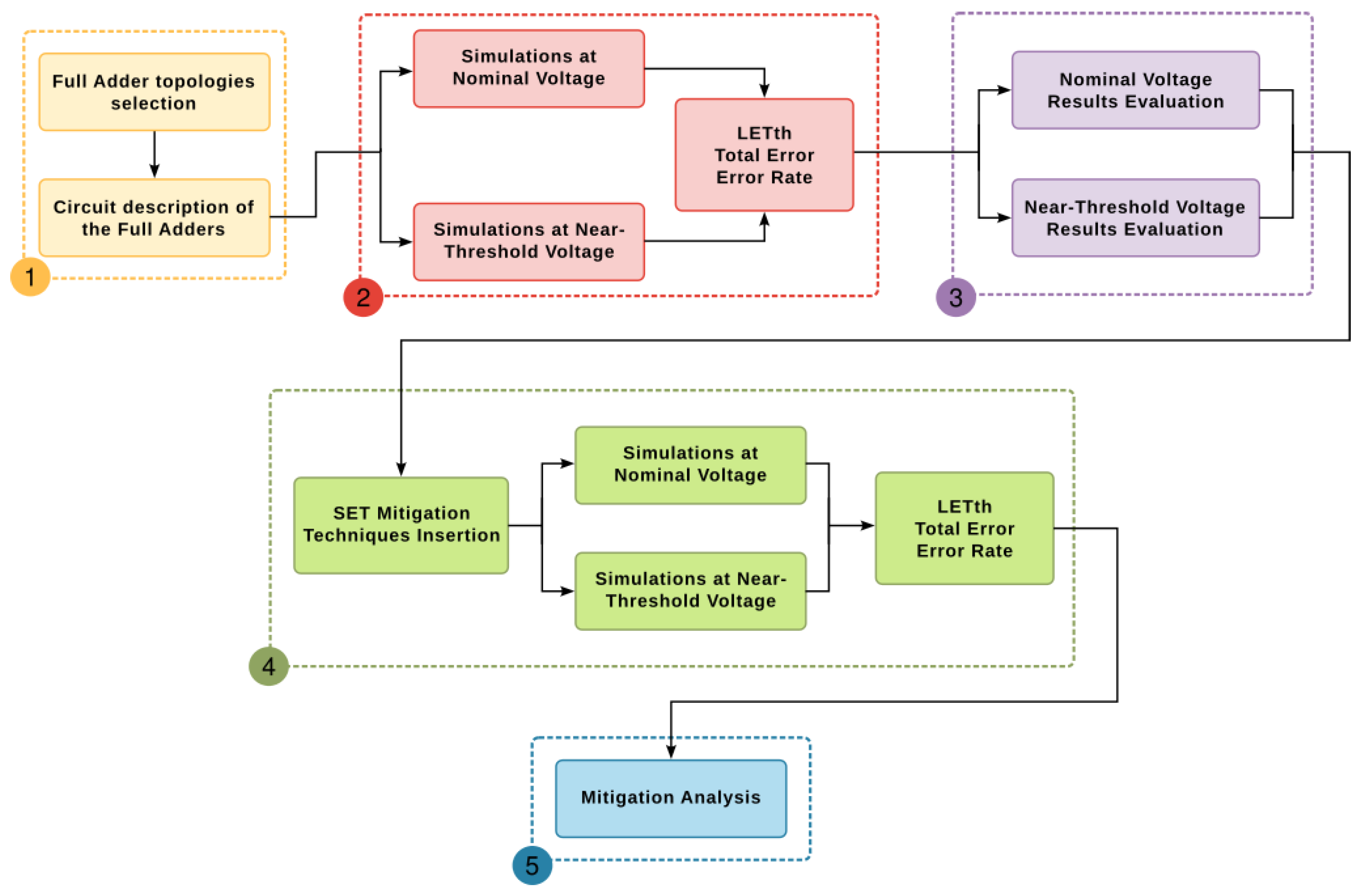
The evaluation of radiation sensitivity begins by testing the circuits at their nominal voltage and subsequently at near-threshold voltage. Throughout this process, LETth values exceeding 100
are used to identify nodes that are not sensitive to single-event transients (SETs).
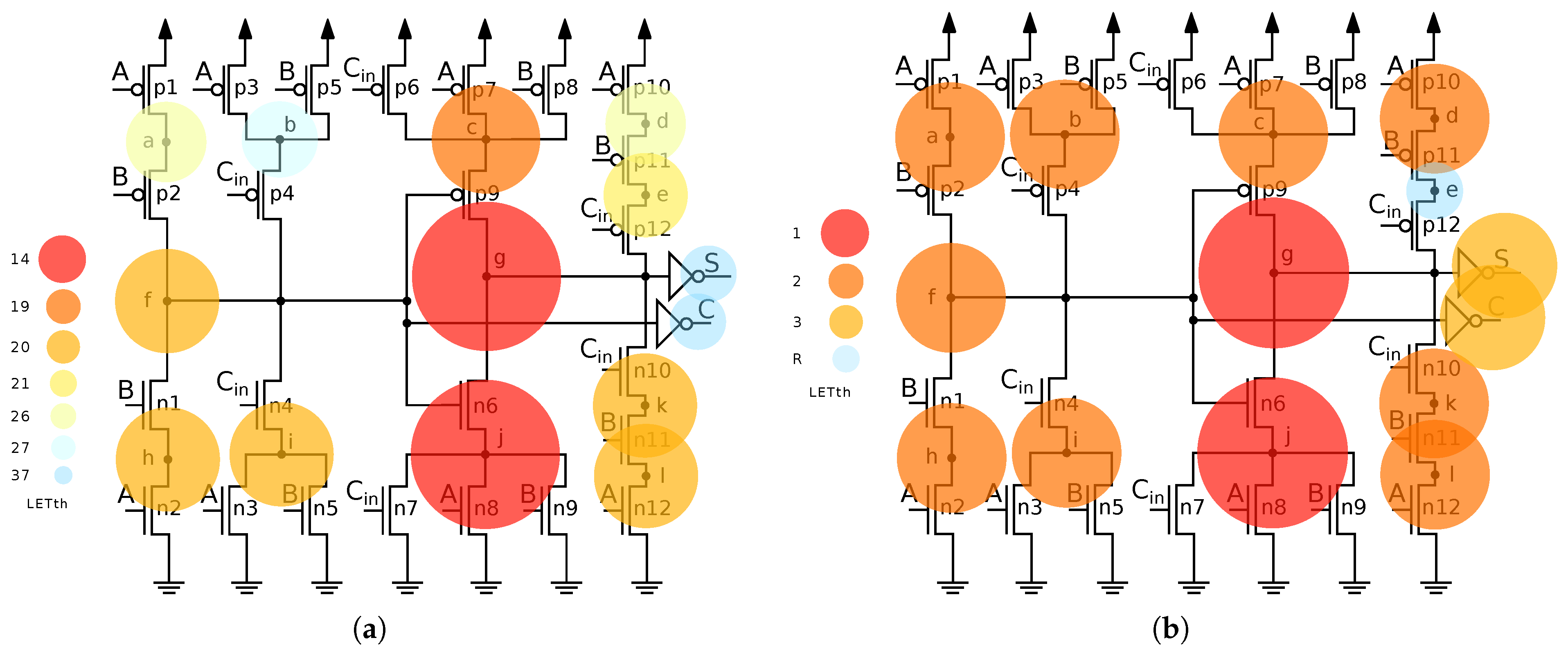
Figure 3,
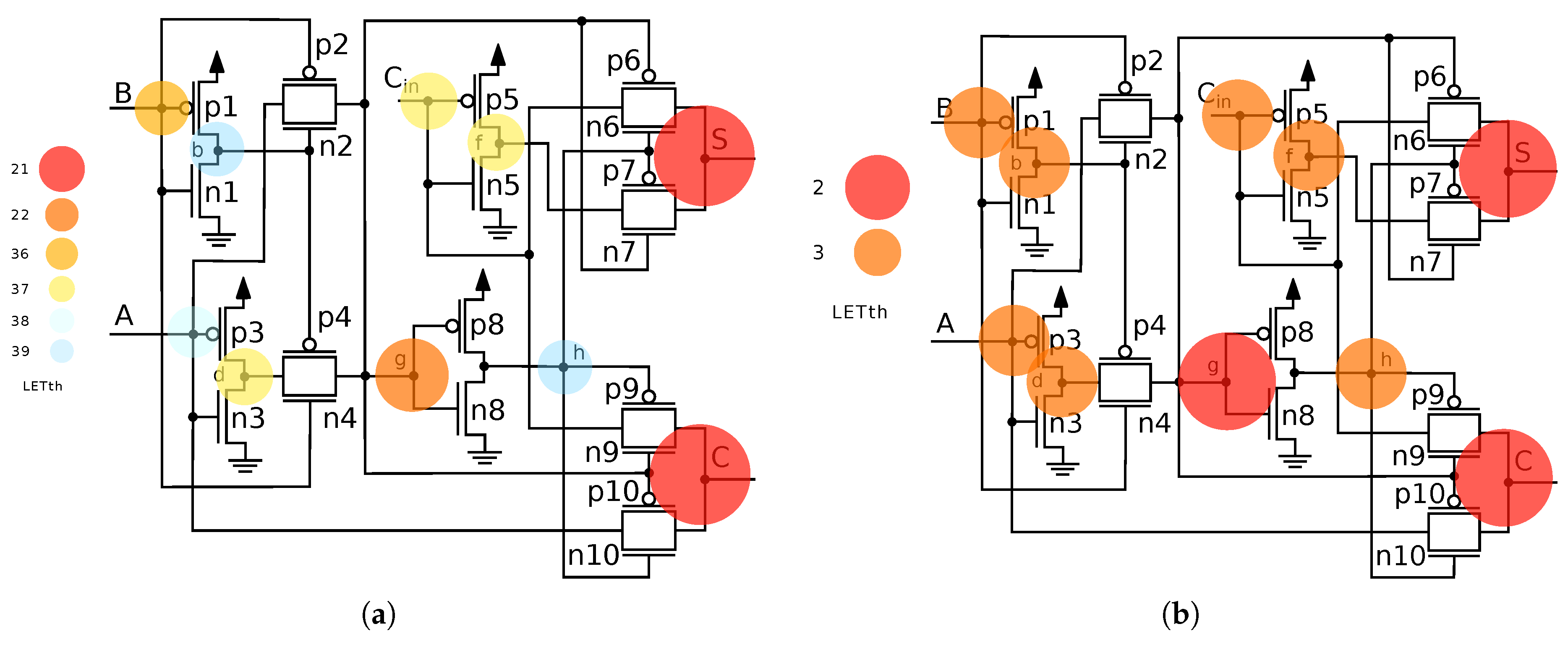
Figure 4,
Figure 5 and
Figure 6 illustrate the LETth values for various circuit nodes, highlighting those deemed critical due to their notably low LETth values. These figures visually represent the data provided in the tables available in the
Supplementary Material, reinforcing the analysis and facilitating interpretation. The
Supplementary Material provides a complete data generated for all the evaluations that we present here. By focusing on these critical nodes, the analysis provides valuable insights into potential vulnerabilities in the circuit’s radiation tolerance, forming the basis for developing targeted mitigation strategies to enhance overall system reliability.
4.1. Critical Nodes
In the Mirror full adder, nodes
g, and
j exhibit the lowest LETth value of 14
, indicating high sensitivity to radiation-induced effects. These internal nodes are particularly critical due to their greater vulnerability compared to others, especially output nodes. Nodes
c,
f,
h,
i,
k and
l show moderate sensitivity, with LETth values ranging from 19 to 20
, as
Table 2 highlights. While less vulnerable than
g and
j, disruptions at these nodes can still impact the circuit’s correctness. Output nodes
Sum and
Cout present significantly higher LETth values of 37
, suggesting lower sensitivity to SETs. This reduced vulnerability may stem from output loading effects that help attenuate transient glitches and prevent error propagation.
Figure 3b further highlights
g and
j as the most SET-sensitive nodes, under reduced voltage operation. Lowering the supply voltage leads to a 14-fold degradation in their LETth, dropping from 14
under nominal conditions to just 1
at NTV operation, presented in
Table S9. These findings underscore the importance of targeting mitigation strategies at these critical internal nodes to enhance the robustness of the Mirror FA.
In the Hybrid full adder, node
c is identified as the most sensitive under nominal voltage operation, as
Table 3 shows, with a lowest LETth value of 8
. This highlights its critical role and heightened susceptibility to SETs. Nodes
b and
d also show notable vulnerability, with LETth values of 12 and 14
, respectively, indicating a significant risk of radiation-induced errors despite being more resilient than node
c. All other nodes demonstrate moderate sensitivity, with LETth values above 20
, suggesting a reasonable tolerance to SETs.
Under NTV operation, as expected, the internal nodes of all evaluated full adders show increased sensitivity under low-voltage conditions. The Hybrid FA sensitivity is depicted in
Figure 4b. Most nodes, including
b,
c, and
d, reach a critical LETth value of 2
, further confirming their vulnerability. In contrast, nodes
Sum,
Cout, and especially
Cin display significantly higher LETth values, with
Cin maintaining a value above 100
and emerging as the least critical node, as shown in
Table S11 from Supplementary Material. This consistent resilience of
Cin across voltage levels suggests a unique robustness within the topology. The use of a combination of complementary logic and pass-transistor logic (PTL) likely contributes to this vulnerability, indicating that this design approach may not be ideal for applications in radiation-prone or noisy environments. Based on these results, nodes
b,
c, and
d are prime candidates for targeted mitigation techniques to improve the radiation tolerance of the Hybrid FA under both nominal and NTV operations.
The radiation-induced error analysis of the TGA FA reveals critical vulnerabilities in specific nodes, particularly under varying operating voltages, as
Table 4 highlights. At NV, the nodes associated with the primary outputs,
Sum and
Cout, exhibit the lowest LETth values, measured at 22
. This identifies them as the most susceptible to SETs, making them the dominant contributors to the circuit’s soft error rate. Node
g also demonstrates comparatively low LET values, further highlighting its potential as a critical site for radiation-induced disruptions. This behavior contrasts with more robust internal nodes such as
h and
b, which show significantly higher LET thresholds, indicating enhanced resilience to transient faults.
A distinguishing factor in this increased vulnerability, particularly at the output stage, is the lack of buffering and the reliance on Pass Transistor Logic in the TGA topology. These design choices reduce signal drive strength and noise margins, rendering output nodes more sensitive to ionizing particle strikes. This is in contrast to other adder architectures, where internal logic nodes typically dominate in terms of criticality.
When the TGA adder operates at NTV, the susceptibility to radiation effects escalates dramatically, illustrated in
Figure 5b. A sharp reduction in the critical LET threshold is observed, dropping from 22
to just 2
, representing over a 21× increase in sensitivity for the same critical nodes. Notably, the Sum and Cout nodes remain the most vulnerable, preserving their critical status under NTV; values are presented in
Table S13 from Supplementary Material. In addition, node
g also emerges as a critical node under these conditions, reaching the same low LET threshold. As illustrated in
Figure 5b, the transition to NTV operation amplifies the effects of design limitations inherent in the TGA architecture. The findings emphasize the necessity of reconsidering output stage design, potentially through the inclusion of radiation-hardened buffers or alternative logic styles, when deploying the TGA full adder in radiation-prone or ultra-low-power environments.
The analysis of the TFA FA under radiation exposure highlights Sum as the most critical node, exhibiting the lowest LET threshold of 14
at nominal voltage, shown in
Table 5. This low value indicates a pronounced vulnerability to single-event transients (SETs) and identifies Sum as the primary contributor to radiation-induced faults in the circuit. In addition, nodes e and Cout also emerge as critical, with LET thresholds of 19 and 21
, respectively. These relatively low values suggest that these nodes are particularly susceptible to ionizing particle strikes, posing a significant threat to the circuit’s reliability. In contrast, nodes b and f exhibit notably higher LET thresholds of 43 and 42
, respectively, indicating a more robust behavior under radiation. These nodes are less likely to propagate transient errors, thus contributing to the overall resilience of the TFA topology.
The LET threshold for Sum at NTV drops from 14 to just 1
, marking a 14× increase in vulnerability, with values presented in the
Supplementary Material in Table S15. Moreover, while Cout was already identified as moderately vulnerable at NV, it now becomes a critical node at NTV, also showing a reduced LET threshold of 2
. These trends are visually captured in
Figure 6.
These findings suggest that while certain nodes within the TFA design exhibit natural resilience, others, particularly the outputs, demand targeted mitigation strategies, such as hardened logic or buffer insertion, to ensure reliable operation in radiation-prone or ultra-low-power environments.
This sensitivity analysis not only informs us about vulnerability in specific nodes but also sets the stage for further exploration into mitigation strategies tailored to enhance the robustness of these critical nodes. As we delve deeper into our study, we aim to correlate these critical nodes with observed errors and Pattern routing investigate potential circuit-level techniques to mitigate the impact of SETs on each FA topology.
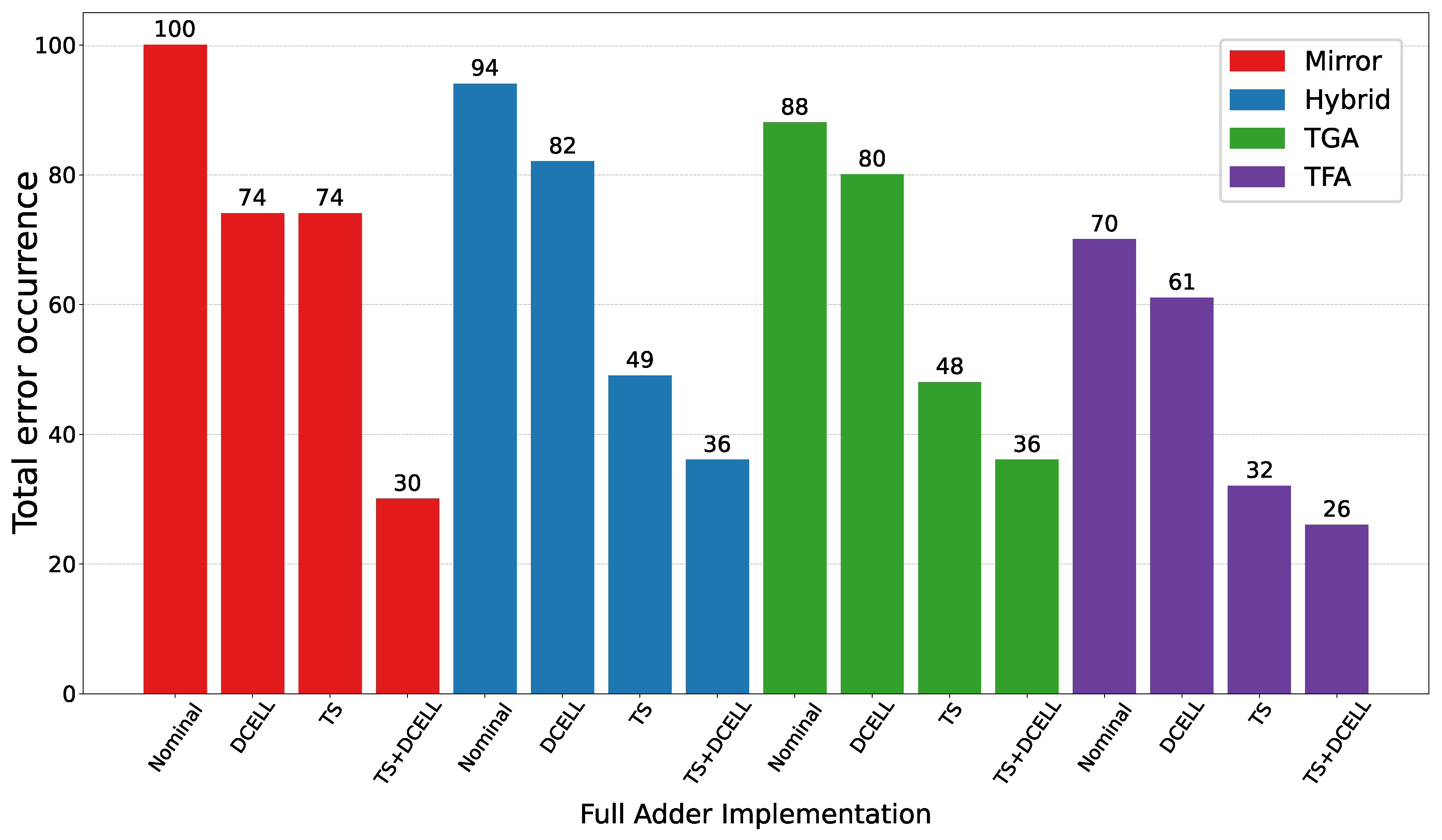
4.2. Error Rate
Based on the total error analysis for each node, we can identify the most and least sensitive nodes. The total error is indicative of the robustness of each node in the face of faults, with lower values signifying less sensitivity. The analysis of LETth for the four evaluated FAs provides critical insights into the sensitivity of individual nodes to transient errors under both nominal and NTV conditions. Under nominal voltage operation, the Mirror FA node
k exhibits the highest susceptibility to error generation, accounting for approximately 12% of all observed transient faults, presented in
Table S1. This highlights its pivotal role in the overall fault profile of the Mirror FA topology. Other nodes, including
e,
f,
g,
l,
Sum, and
Cout, also demonstrate moderate sensitivity, each contributing between 8% and 9% of the total error occurrences. These nodes are notably affected by variations in input pulse conditions. Nodes that are topologically distant from the outputs tend to be more resilient against transient faults. This increased robustness can be attributed to the ability of the transistor network to attenuate signal glitches, particularly in nodes driven by multiple transistors. For example, nodes
b,
c,
i, and
j exhibit lower fault sensitivity, indicating an inherent resistance to error propagation. When operating at NTV, the total number of transient faults increases significantly, by approximately 19%, compared to nominal conditions, as shown in
Table S9 from Supplementary Material. Notably, node
a, which was relatively robust at nominal voltage, becomes substantially more error-prone under NTV, contributing to around 11% of all computed errors. Furthermore, nodes
d,
h, and
i also emerge as significant contributors to output interference at NTV, revealing shifts in the error distribution profile due to voltage scaling. In summary, node
k plays a central role in fault susceptibility under nominal conditions, while nodes
e,
f,
g,
l,
Sum, and
Cout exhibit moderate sensitivity to transient errors. In contrast, nodes farther from the outputs, such as
b,
c,
i, and
j, demonstrate higher resilience, likely due to glitch attenuation along their paths. At near-threshold voltage, previously resilient nodes like
a becoming significantly more error-prone. Errors more frequently propagate to the
Sum output, indicating that the internal structure offers greater protection to the
Cout path.
On the Hybrid FA under NV, nodes
c and
d emerge as the most sensitive components, showing the highest probabilities of generating transient faults, as presented in
Table S3 from Supplementary Material. Nodes
a,
e,
f,
h,
i,
j,
Sum, and
Cout demonstrate similar, moderately sensitive behavior, contributing comparably to the overall error profile. Notably, node
Cin displays exceptional robustness, with zero observed errors across all evaluated pulse scenarios, suggesting its fault resilience is context-independent. These findings offer a comprehensive perspective on fault propagation paths within the Hybrid FA and provide a foundational basis for exploring fault mitigation strategies to reinforce its most vulnerable nodes. As shown in
Table S11 from Supplementary Material for the Hybrid FA evaluated under NTV conditions, nodes
a,
b,
d,
f, and
g exhibit substantial sensitivity to soft errors, each contributing close to 10% of the total fault occurrences. Among these, node
d stands out as the most vulnerable, responsible for approximately 12% of all recorded errors at NTV. Collectively, these five nodes account for nearly 50% of total transient faults, marking them as critical points of failure. Furthermore, a comparison with nominal voltage results highlights a significant increase of 33% in total error occurrences at NTV. Overall, the Hybrid FA demonstrates a diverse sensitivity profile across different nodes, with node
d consistently ranking among the most susceptible at both voltage levels. While some nodes maintain moderate fault sensitivity, the sharp rise in error rates under NTV—particularly among nodes
a,
b,
d,
f, and
g—emphasizes the need for topology-aware fault mitigation strategies. The robustness of node
Cin remains noteworthy, serving as a potential architectural reference for designing more resilient logic paths.
The LETth analysis of the TGA FA highlights nodes
b,
h and
Cout as the most vulnerable under both nominal and NTV conditions, jointly contributing to about 39% of all transient faults. This emphasizes their critical role in error propagation within the TGA topology. Unlike other FA configurations, TGA shows reduced output-level robustness, with
Sum being more prone to SETs than many internal nodes. Additionally, nodes
Sum and
g show moderate sensitivity that varies with input pulse conditions. Although node
Sum may appear less sensitive in specific cases (e.g., under pulse 001), its cumulative fault contribution confirms its criticality in the overall fault profile. When operating under NTV conditions, the TGA FA experiences a substantial degradation in reliability, with a 39% increase in total error occurrences compared to nominal voltage, as shown in
Table S13. In this scenario, node
h emerges as error-prone, exhibiting a slight increase in sensitivity—approximately 1% more than nodes
Cin and
Cout. Despite this shift, nodes
h and
Sum remain among the most critical contributors to overall errors. Furthermore, nodes
Cout and
e display a notable increase in sensitivity under NTV, warranting their inclusion in the critical node set for fault mitigation considerations. These findings indicate that the TGA FA topology is particularly vulnerable at the output nodes, with
h and
Cout consistently ranking as the most sensitive components under both voltage regimes. Nodes
b,
g, and
Cout show moderate to high sensitivity, depending on the operating condition and pulse pattern. The significant rise in error rates at NTV, particularly from nodes
b,
h, and
Cout, highlights the necessity of robust fault-tolerant design strategies to ensure reliable operation in low-voltage environments.
Similar to the behavior observed in the TGA topology, one of the most vulnerable nodes in the TFA design is the output node
Cout, which consistently emerges as a critical point of failure, as results presented in
Table S7 from Supplementary Material. This recurring sensitivity in output nodes across both topologies may stem from the lack of buffering at the output stage, as suggested by the structural layouts in
Figure 6. At nominal voltage, nodes
e and
Cout each account for approximately 14% of the total error count, indicating a high level of fault sensitivity. Additionally, nodes positioned near the outputs show elevated susceptibility, with error rates that in some cases approach those of the most critical nodes. The behavior of node
Sum is notably variable, exhibiting sensitivity that fluctuates depending on the input pulse scenario, thereby highlighting the need for a context-specific assessment to fully understand its role in transient fault propagation. Under NTV operation, the TFA FA topology experiences the most severe degradation among all topologies analyzed, with a marked increase of over 54% in total error occurrences, as shown in
Table S15 from Supplementary Material. In this low-voltage regime, node
b remains the most susceptible, contributing 14% of the total errors, while nodes
e and
Cout also emerge as critical fault sources, each accounting for approximately 13% of the total errors. This consistent vulnerability of output-related nodes across voltage levels highlights a systemic weakness in the TFA design, necessitating the development of targeted fault mitigation strategies, particularly under reduced voltage conditions. The context-dependent nature of node
Sum adds complexity to the analysis, reinforcing the need for comprehensive, pulse-specific evaluation methods. Overall, the TFA’s high error increases under NTV positions; it is the least robust among the full adder designs examined in this study.
4.3. Input Vectors
In the context of a FA circuit, an input vector combination refers to a specific arrangement of input values applied to the circuit to perform a computation. In the realm of radiation hardness, the sensitivity of a circuit to radiation events can vary depending on the specific combination of input vectors applied. Certain input vector combinations may lead to conditions where the circuit is more vulnerable to radiation-induced errors [
52].
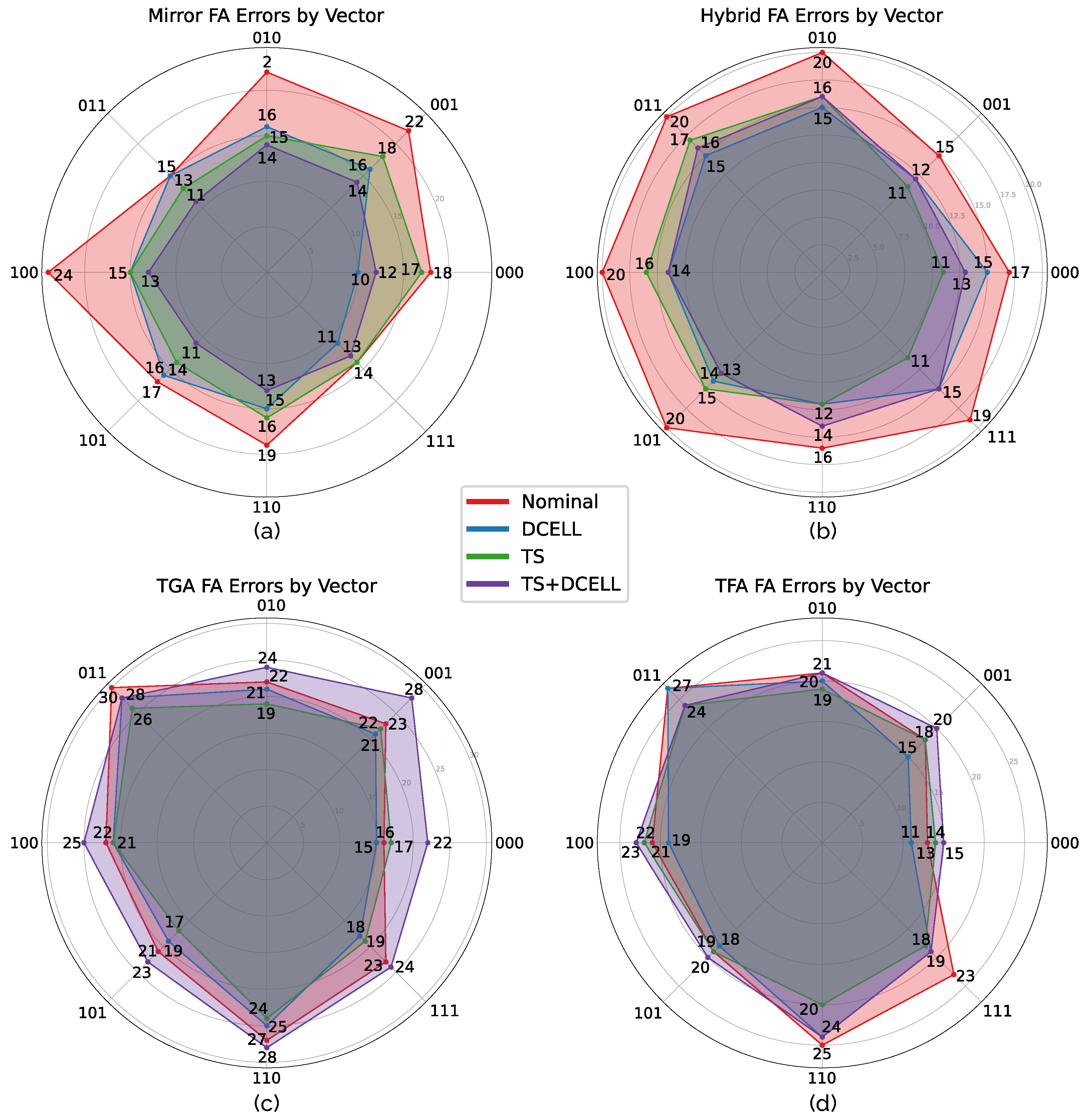
For the Mirror FA operating at NV, 14% of the total errors manifest in response to the input vector 011, presented in
Table S2 from Supplementary Material. Vector 100 also contributes significantly to error propagation, albeit with a slightly lower rate of 12%. The critical LETth values are associated with the input vector 000, establishing it as the pivotal input combination with the lowest LETth and, consequently, the most critical for the Mirror circuit under nominal conditions. Under NTV operation, the error behavior shifts. Input vector 100 exhibits the highest susceptibility to error generation, as shown in
Table S10 from Supplementary Material. Furthermore, vectors 001 and 010 contribute notably to error propagation, together accounting for over 46% of the total SET occurrences. Consistent with nominal voltage operation, vector 000 maintains the lowest LETth, reaffirming its role as the most critical input combination for the Mirror topology across both voltage domains.
Shifting focus to the Hybrid FA, a distinct pattern in error behavior is observed under different operating voltages. At nominal voltage, the input vector 000 exhibits the lowest error rate, accounting for only 8% of the total error occurrences, while vector 011 demonstrates the highest error rate at nearly 15%, results available in
Table S4 from Supplementary Material. Notably, vector 001 is associated with the lowest LETth, identifying it as the critical input combination for this topology under nominal conditions. Under NTV operation, the error profile shifts slightly, as presented in
Table S12 from Supplementary Material. Input vectors 010, 011, 100, and 101 each present a high and nearly uniform error rate of approximately 14%, indicating increased vulnerability to error generation in the NTV regime. These same vectors are linked to the lowest LETth values under NTV conditions, designating them as the most sensitive inputs for the Hybrid FA at reduced supply levels. Consistent with the nominal case, vector 000 remains the most resilient, once again displaying the lowest error rate at just 8%.
For the TGA FA, the input vector 011 emerges as the most error-prone under both nominal and NTV conditions. At nominal voltage, vector 011 accounts for approximately 17% of the total error occurrences and is also associated with the critical LETth value. Interestingly, aside from the 000 input vector, all other input combinations eventually reach a LETth of 21 MeV · cm
2/mg, indicating that for this topology, the critical LET threshold is largely independent of specific input combinations. When operating at NTV, the error distribution remains similarly concentrated around vector 011, which contributes 16% of the total SET events, reinforcing its status as the most sensitive input. Furthermore, as shown in
Table S14, multiple vectors share the lowest LETth value of 2 MeV · cm
2/mg, including vectors 001, 010, 011, 100, 101, and 111. This suggests a broader vulnerability across different input combinations at lower voltages, depending on the specific node affected by radiation. As observed in the Hybrid and Mirror topologies, vector 000 consistently presents the lowest error rate, confirming its robustness under both operating conditions.
For the TFA FA, the input vector 011 is consistently among the most error-prone across both voltage domains, presented in
Table S8. At nominal voltage, this vector accounts for approximately 18% of the total error occurrences, highlighting its high susceptibility to transient fault generation. However, the critical LETth values for this topology are associated with the input vectors 010 and 100, rather than 011. Meanwhile, vector 000 stands out as the most robust input combination, contributing only 6% of the total observed errors. Under reduced voltage conditions the TFA topology experiences a more pronounced sensitivity to radiation-induced disturbances. As shown in
Table S16 from Supplementary Material, vectors 010 and 100 become even more critical, with LETth values dropping to just 1
, indicating a heightened vulnerability at reduced supply levels. Despite this, vector 011 remains the most error-prone, contributing up to 21% of the total SET events, thus reaffirming its status as the most sensitive input vector under NTV operation. Consistent with the nominal case, vector 000 continues to demonstrate the lowest error rate, underscoring its robustness across both operating conditions.
This comprehensive analysis of input vectors sheds light on specific combinations that significantly influence error rates, aiding in the identification of critical scenarios and potential avenues for targeted mitigation strategies. The findings aid in identifying critical scenarios and offer potential avenues for targeted mitigation strategies.
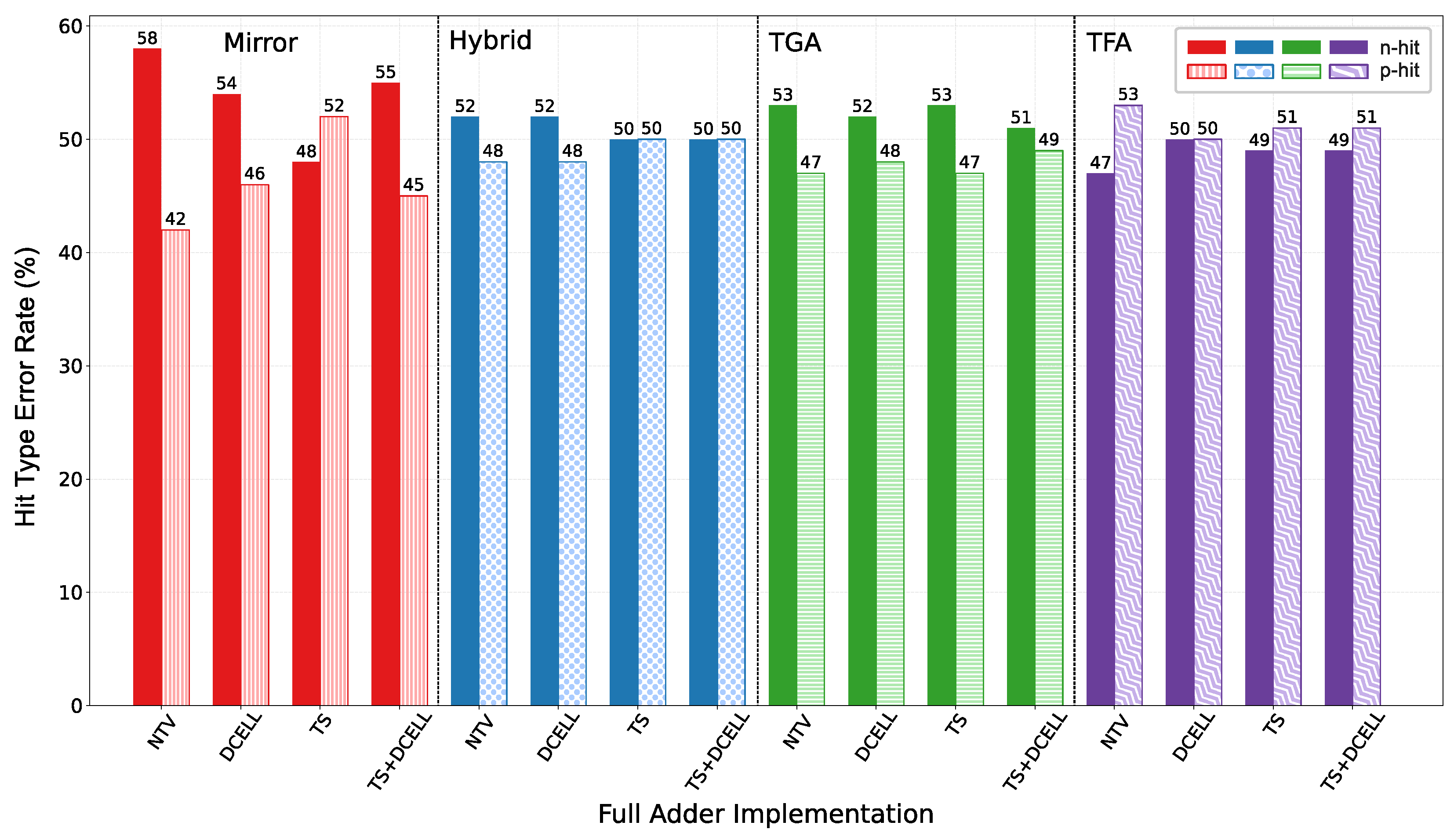
4.4. Type of SEE Hit
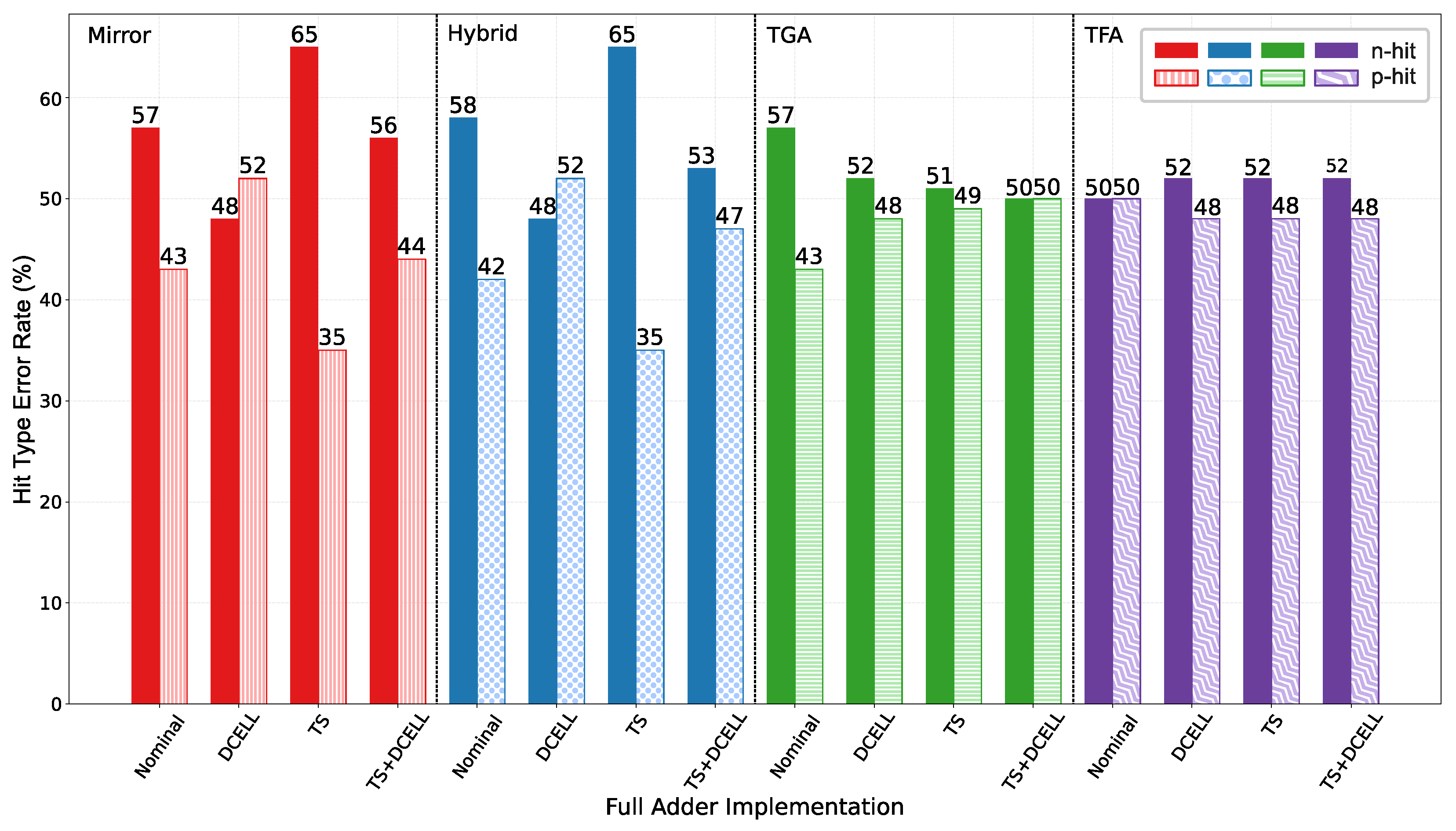
In the context of radiation-induced effects on digital circuits, different electrical pulse types, specifically observing the n-hit and p-hit effects, result from the interaction of energetic particles with the circuit components.
Examining the impact of different radiation hits on the Mirror FA, the n-hit emerges as the most critical pulse type under both nominal and NTV operations. At nominal voltage, the n-hit generates the lowest LETth values across all outputs, underscoring its significance in inducing transient errors. This pulse type is responsible for nearly 57% of the total transient errors observed in simulations, a rate that is up to 20% higher than that associated with the p-hit, further emphasizing the dominant role of n-hits in error propagation. For the NTV conditions, the n-hit remains the critical SET pulse, accounting for approximately 58% of the total observed SET events across the combined Sum and Cout outputs. It continues to produce the lowest average LETth values for both outputs, reinforcing its criticality in low-voltage operation. These findings demonstrate the persistent dominance of n-hits in error generation for the Mirror FA, irrespective of the supply voltage.
The analysis of the Hybrid FA reveals that n-hits are the primary contributors to error generation across both nominal and NTV conditions. At nominal voltage, n-hits account for approximately 58% of the total errors, making them the dominant source of transient faults in this topology. This hit type not only generates the highest error rate but also corresponds to the critical LETth values, exhibiting the lowest LETth on average. When operating at NTV, the trend persists, with n-hits maintaining a slightly higher error rate compared to p-hits and remaining responsible for the critical LETth values. The 58% error contribution from n-hits highlights their continued significance in influencing the overall error susceptibility of the Hybrid FA at reduced supply voltages. These results underscore the dominant role of n-hits in shaping the error characteristics of the Hybrid topology, irrespective of the operating voltage.
In the TGA FA, the n-hit is the predominant cause of transient errors across both nominal and NTV operations. At nominal voltage, n-hits are responsible for up to 57% of total errors, with 44% of these manifesting specifically at the Sum output. This highlights the criticality of the n-hit in this topology, likely due to signal paths that are more vulnerable to charge deposition and resultant transient faults during high-to-low pulse transitions. During NTV operation, the n-hit remains the most significant contributor, accounting for 53% of total error occurrences. However, both n-hits and p-hits generate critical LETth values, particularly when the radiation strike impacts the Sum node. This indicates that the Sum output is sensitive to both types of hits in the TGA topology, emphasizing a broader susceptibility to transient errors at reduced supply voltages.
In contrast to the other examined topologies, the Transmission Gate Full Adder (TFA) exhibits a distinctive and balanced response to radiation-induced transient errors across both n-hit and p-hit types. At nominal voltage, error rates for both hit types are approximately 50%, indicating a symmetric vulnerability to transient faults. Analyzing individual outputs, the Cout node consistently shows an error rate around 17%, while the Sum output is more susceptible, with error rates reaching about 34% for both hit types. This uniform distribution suggests that the TFA topology is equally affected by radiation pulses, causing both rising and falling transitions. Under NTV conditions, the error profile shifts, with n-hits significantly increasing their impact and accounting for nearly 53% of total errors observed. Notably, the high-to-low (n-hit) pulses are responsible for generating all critical LETth values during the simulations, highlighting the growing dominance of n-hit-induced errors at reduced supply voltages. This behavior underscores a voltage-dependent shift in the TFA’s susceptibility to radiation, favoring n-hit effects under NTV operation.
4.5. Evaluation Overview
Examining circuits across diverse corner scenarios sheds light on potential techniques to enhance robustness in both operational contexts. This analysis seeks to uncover the nuances of how circuits react to varying voltage conditions. Identifying critical nodes, components, and operational behaviors becomes crucial in this exploration. These insights are fundamental for customizing effective mitigation strategies to fortify the resilience of FA circuits across diverse scenarios of operation. The results found across both voltage scenarios are summarized in
Table 6.
When comparing the two voltage operations for the Mirror FA, the most susceptible node can vary depending on the scenario analyzed. However, it is noteworthy that the node Cout consistently exhibits the highest susceptibility rate in both scenarios. On the other hand, nodes k and l also warrant attention for improving robustness regarding voltage operations due to their high susceptibility to propagate radiation events. In the case of the Hybrid FA, error susceptibility is more balanced among nodes, with several nodes exhibiting approximately the same error rate. Notably, among the different voltage scenarios analyzed, nodes a, c, d, and f stand out as the most susceptible to propagate interference noise to the outputs. Examining the TGA topology reveals that, despite some nuances across different voltage operations, nodes b, h, sum, and cout consistently remain among the most susceptible nodes to propagate SET errors. In the case of the TFA topology, nodes d, e, and cout consistently maintained critical values. It is noteworthy that node e remained the most susceptible to propagate errors regardless of the voltage operation.
In terms of input vectors, different combinations show varying error rates. In the case of the Mirror FA at NTV, vector 100 emerges as the most error-prone. For the Hybrid FA, vectors 010, 011, 100, and 101 exhibit similar error rates. The TGA topology indicates that vectors 010 and 011 have higher error rates. In contrast, the TFA topology shows that vectors 010 and 011 are more prone to propagating errors. Critical input vectors are identified as follows: 000 for the Mirror FA, 001 for the Hybrid FA, and, for the TGA, all inputs except for vectors 00 and 101 can propagate the lowest LETth values. Lastly, the TFA topology designates vector 100 as the critical input, as it consistently results in the lowest LETth values across experiments.
Concerning SET hit types, the n-hit consistently emerges as critical for all topologies analyzed under both voltage operation conditions, except for the TFA topology in NTV operation, where the pulse n-hit exhibits a higher error rate. However, it is noteworthy that the critical LETth values are predominantly generated by the n-hit across the various scenarios.
Critical nodes vary between the FA topologies. For the Mirror FA, nodes g and j remain the most sensitive in both voltage operations. In the Hybrid FA, despite a higher increase in critical nodes in NTV, nodes c and d consistently exhibit the lowest LETth in both scenarios. In the TGA topology, nodes Sum and Cout consistently emerge as critical in propagating SETs regardless of the voltage scenario. Finally, for the TFA, nodes e and Sum stand out as critical nodes, presenting the lowest LETth values in both scenarios.
In conclusion, the voltage comparison across various FA topologies revealed nuanced sensitivities and critical nodes under different operating conditions. Each topology exhibited distinct responses to voltage variations, emphasizing the importance of tailored mitigation strategies. Analyzing these scenarios provides valuable insights into our investigation and enables us to explore strategies for optimizing robustness and reliability in integrated circuits facing diverse voltage conditions, contributing to the advancement of radiation-hardened circuit design.


