Article

High-Efficiency and Cost-Effective 10 W Broadband Continuous Class-J Mode Quasi-MMIC Power Amplifier Design Utilizing 0.25 μm GaN/SiC and GaAs IPD Technology for 5G NR n77 and n78 Bands

1
Department of Electrical Engineering, National Central University, Taoyuan City 320317, Taiwan
2
Taiwan Semiconductor Research Institute, National Applied Research Laboratories, Hsinchu 300091, Taiwan
*
Author to whom correspondence should be addressed.
Electronics 2023, 12(16), 3494; https://doi.org/10.3390/electronics12163494
Submission received: 27 July 2023 / Revised: 16 August 2023 / Accepted: 16 August 2023 / Published: 17 August 2023
(This article belongs to the Special Issue Microwave/Millimeter-Wave Power Amplifiers)

Abstract

:
This paper presents two power amplifiers designed for 5G NR n77 and n78 bands. These power amplifiers were fabricated using WINTM Semiconductors’ 0.25 μm GaN/SiC technology and GaAs IPD technology. To achieve a reduction in costs, GaAs IPD technology was incorporated in the design, leading to the realization of a quasi-monolithic microwave integrated circuit design. To ensure high power, high efficiency, and broadband operation, a continuous Class-J mode output matching network was utilized. The power amplifier with split chip-on-board wire-bond assembly had a power gain of 21.7 dB, a 3 dB power bandwidth ranging from 2.85 GHz to 4.48 GHz, a saturation power of 40.3 dBm, and a peak power-added efficiency of 39.5%. On the other hand, the power amplifier with stack chip-on-board wire-bond assembly had a power gain of 21.7 dB, a 3 dB power bandwidth ranging from 2.84 GHz to 4.47 GHz, a saturation power of 40 dBm, and a peak power-added efficiency of 36.5%. For a 5G NR FR1 256-QAM 100-MHz bandwidth modulated signal with a frequency range of 3.3 GHz to 4.2 GHz, both the split and stack chip-on-board wire-bond assembly power amplifiers achieved average output powers of 29.6 dBm and 28.3 dBm, respectively. These output powers were measured under an error vector magnitude requirement of 3.5%.

1. Introduction

The fifth generation (5G) of mobile network technology offers high-speed data transmission, low latency, and a high data rate. It facilitates various applications, including multimedia services like high-definition video streaming as well as Internet of Things (IoT) applications, thus enabling the development of smart homes, smart cities, and autonomous driving. The expansion of 5G networks has led to a surge in demand for microcells in indoor settings such as homes, offices, factories, and warehouses. These microcells require radio frequency (RF) power in the range of 1–10 W to provide coverage over distances of 30–1000 m [1,2]. Because microcells are typically powered by fixed cables, the supply voltage (which is typically around 4.2 volts) will not be limited by lithium-ion batteries. Utilizing higher supply voltages from the fixed power source enables the use of power amplifiers (PAs) that require higher voltages for efficient and high-power operation.
While complementary metal oxide semiconductor PAs are cost-effective and commonly used in consumer products, they lack the linearity, efficiency, and output power needed for higher-power applications. Gallium arsenide (GaAs) heterojunction bipolar transistors and pseudo-morphic high-electron-mobility transistors (HEMT) offer higher power density and gain. GaAs technology is traditionally used in RF PAs [3,4]. However, for sub-6 GHz microcell applications that require high output power, gallium nitride (GaN) HEMT technology offers clear advantages. GaN HEMT technology’s wide bandgap, high electron saturation velocity, and high breakdown voltage enable higher RF output power due to higher DC voltage and power density compared to GaAs HEMT technology. GaN HEMT has seen a significant rise in its utilization across various applications [5,6].
The use of discrete GaN HEMT components can achieve high performance and cost effectiveness [7,8,9]. However, for size-sensitive microcells, monolithic microwave integrated circuits (MMICs) and quasi-MMIC PAs are preferred. Despite the advantages of MMIC design in achieving a compact size, the cost of a fully integrated solution is relatively high. This cost consideration could pose challenges in meeting the demands of large-scale installations required by infrastructure providers. As a result, quasi-MMIC PAs with GaAs integrated passive device (IPD) technology are preferred for size-sensitive and price-sensitive microcells. They offer a balance between performance and cost effectiveness compared to MMIC designs with expensive GaN/SiC wafers. These quasi-MMIC PAs provide excellent performance while meeting size constraints and remaining cost-effective, making them an attractive choice for microcell applications [10,11,12,13,14,15].
The Doherty power amplifier design is known for maintaining high efficiency at large output power back-offs. However, it faces challenges in achieving wide bandwidth due to the use of a load modulation network, which limits its frequency coverage [16]. Harmonic tuning can improve the efficiency of PAs, but it is limited by bulky quarter-wave transmission lines and LC resonators, affecting the operating bandwidth and chip area [17]. To achieve wide bandwidth without such limitations, continuous mode designs have been employed [18,19,20]. These continuous mode designs utilize simple matching networks, allowing for a broader frequency range and more efficient power amplification over a wider bandwidth.
In this paper, two high-power high-efficiency broadband GaN quasi-MMIC PAs are introduced. The proposed PAs were fabricated in WINTM Semiconductors’ 0.25 μm GaN/SiC HEMT technology and GaAs IPD technology. A continuous Class-J mode output matching network was designed to achieve excellent output performance. The chip-on-board (CoB) wire-bond assembly method was employed to ensure stability and efficient heat dissipation. The split design PA achieved a peak power of 40.3 dBm, while the stack design PA reached a peak power of 40 dBm. For a 5G NR FR1 256-quadrature amplitude modulation (QAM) 100 MHz bandwidth test signal, the average power output for the split design PA was 31.8 dBm, and for the stack design PA, it was slightly lower at 31.5 dBm. The experimental findings are summarized and then compared with the results obtained from studies that have been previously published.

2. Circuit Design

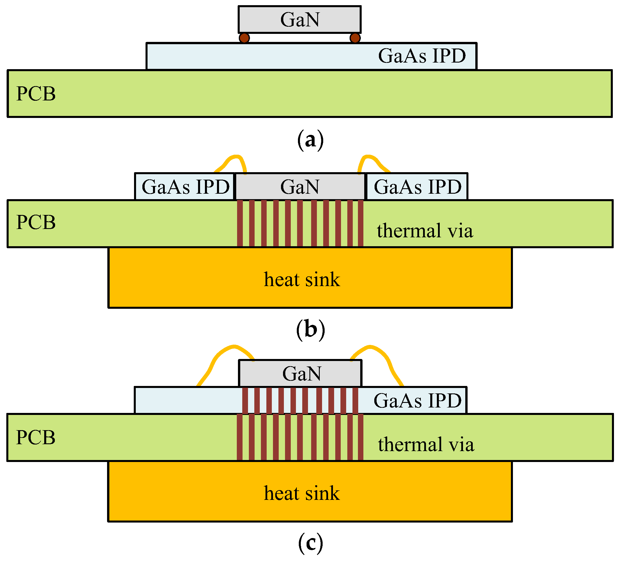
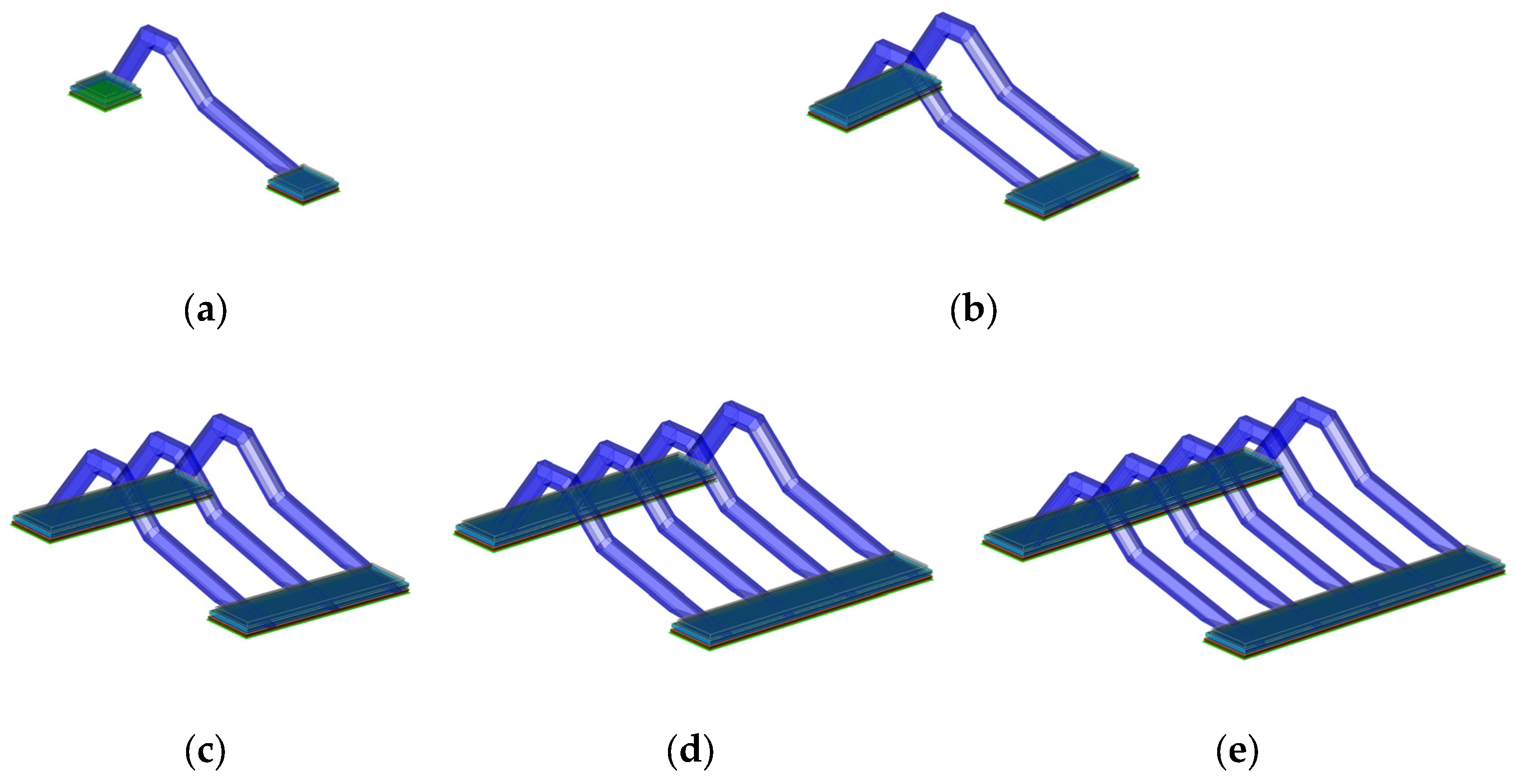
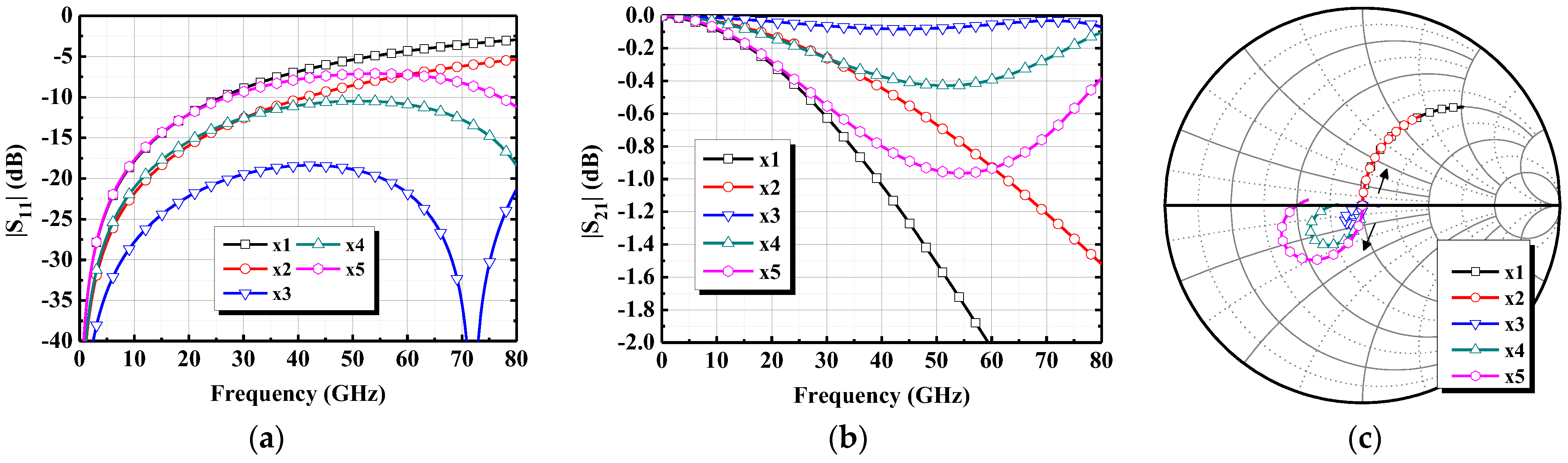
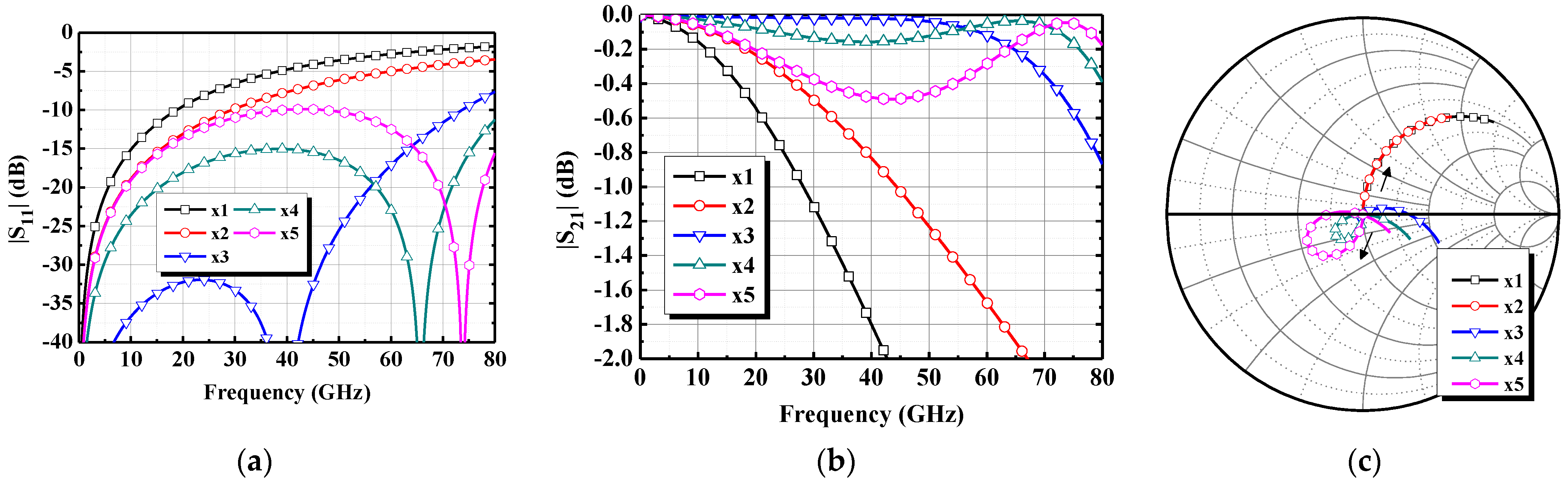
2.1. Assembly and Interconnect Design

For a quasi-MMIC PA design, the authors have the option to choose between flip-chip and CoB wire-bond assembly methods, as depicted in Figure 1. However, considering the target output power of 10 W, it becomes crucial to account for heat dissipation capabilities. Due to the complexity of attaching a heat sink on a flip-chip assembly during RF probing measurements, the authors opt for split and stack CoB wire-bond assembly methods, as shown in Figure 1b,c. In this approach, the substrate printed circuit board (PCB) and heat sinks will efficiently dissipate heat for the output-stage GaN transistors.
For the Class-J output matching network (OMN) design, harmonic frequencies should be considered. In order to minimize the bandwidth impact of bond wire interconnects, a proper wire-bond configuration should be employed. There are several bond wire interconnect designs that can improve bandwidth [21,22,23]. However, those designs are for low-power signal traces. When it comes to high-power high-current design, multiple bond wires should be used. The different bond wire topologies are simulated using the Keysight Advance Design System (ADS) Momentum 3D finite element method (FEM). Figure 2 shows simulation settings of 300 μm length bond wires with different quantities ranging from 1 to 5. The bond wire diameters are 1.0 mil, and the bond ball diameters are 55 μm. As a result, the designed spacing between the bond wires is 100 μm. Therefore, the designed bond pad lengths are 50 μm, and the widths range from 50 μm to 450 μm.
The 3D FEM simulated results of 300 μm length bond wire designs are shown in Figure 3. Figure 3a,b displays the |S11| and |S21| of different designs with different quantities of bond wire. At first, one-bond-wire design, which has the highest inductance, is the worst in |S11| and |S21|. When the quantity is increased to 2 and 3, the results are better. When the quantity is increased to 4 and 5, the results are worse. Thus, the three-bond-wires design has the best results both in |S11| and |S21|. Figure 3c displays the |S11| trajectory in the Smith chart, which is similar to [21]. The bond pad widths increase with the bond wire quantity. Therefore, the parasitic capacitances also increase. The imaginary parts of one- and two-bond-wires designs go positive. On the other hand, the imaginary parts of four- and five-bond-wires designs go negative. The three-bond-wires design has the best combination of inductances and capacitances. Although the three-bond-wires design’s bandwidth is narrower than [21], the total chip area is much smaller. Therefore, the 300 μm length three-bond-wires design can facilitate high-current capacity and wide bandwidth at the same time.
Figure 4 shows the 3D FEM simulated results of 400 μm length bond wire designs with different bond wire quantities ranging from 1 to 5. The three-bond-wires design yielded the best results both in |S11| and |S21|. Although the bandwidth of 400 μm length design is narrower than that of 300 μm length design, it is still appropriate for current circuit design. Thus, the following design steps could use three bond wires with 300–400 μm lengths.

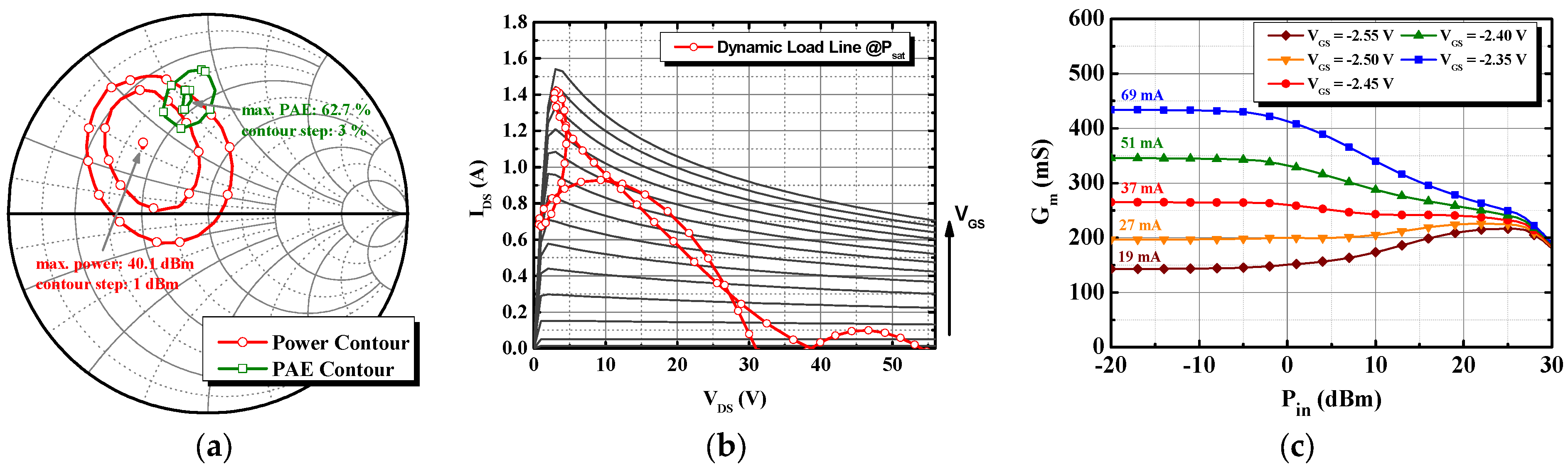
2.2. Transistor and Bias Selection

From the WINTM Semiconductors technology introduction documents, the 0.25 μm gate GaN technology is manufactured on 100 µm SiC substrate. The verified 2 × 125 µm gate channel width transistor of the process performs saturated power density of 5 W/mm at 10 GHz; VD = 28 V, and ID = 100 mA/mm. In order to obtain over the desired 8 W output power, the total gate channel width of 2000 µm was selected. Then, the maximum stable gain (MSG), maximum available gain (MAG), and short circuit current gain (hFE) versus frequency are simulated by the 10 × 200 µm transistor. The results show the maximum frequency of oscillation (fMAX) is higher than 60 GHz. The cut-off frequency (fT) is higher than 20 GHz. Since the fT and fMAX are much higher than the desired n77 and n78 bands of 3.3–4.2 GHz, the RF operation of the 10 × 200 µm transistor was assured. In the load-pull simulation, the 10 × 200 µm transistor obtains 40 dBm output power at the 3-dB compression point (OP3dB), as Figure 5a shows. Figure 5b presents the dynamic load line, with a VGS range from 0 V to −2.6 V in steps of 0.2 V. Thus, the large-signal output performance was also assured.
GaN HEMT usually suffers from the soft gain compression phenomenon. While the gains of other processes’ transistors compress at high power levels, the gains of GaN HEMT compress very early. In order not to increase amplitude-modulation-to-amplitude-modulation (AM–AM) and amplitude-modulation-to-phase-modulation (AM–PM) distortions, an optimal bias point must be carefully determined [24]. Figure 5c showcases the large-signal transconductance (Gm) response for the 10 × 200 µm transistor. Notably, a gate current of 27–37 mA could cause a fairly flat Gm response. Thus, the gate voltage is determined by −2.47 V.

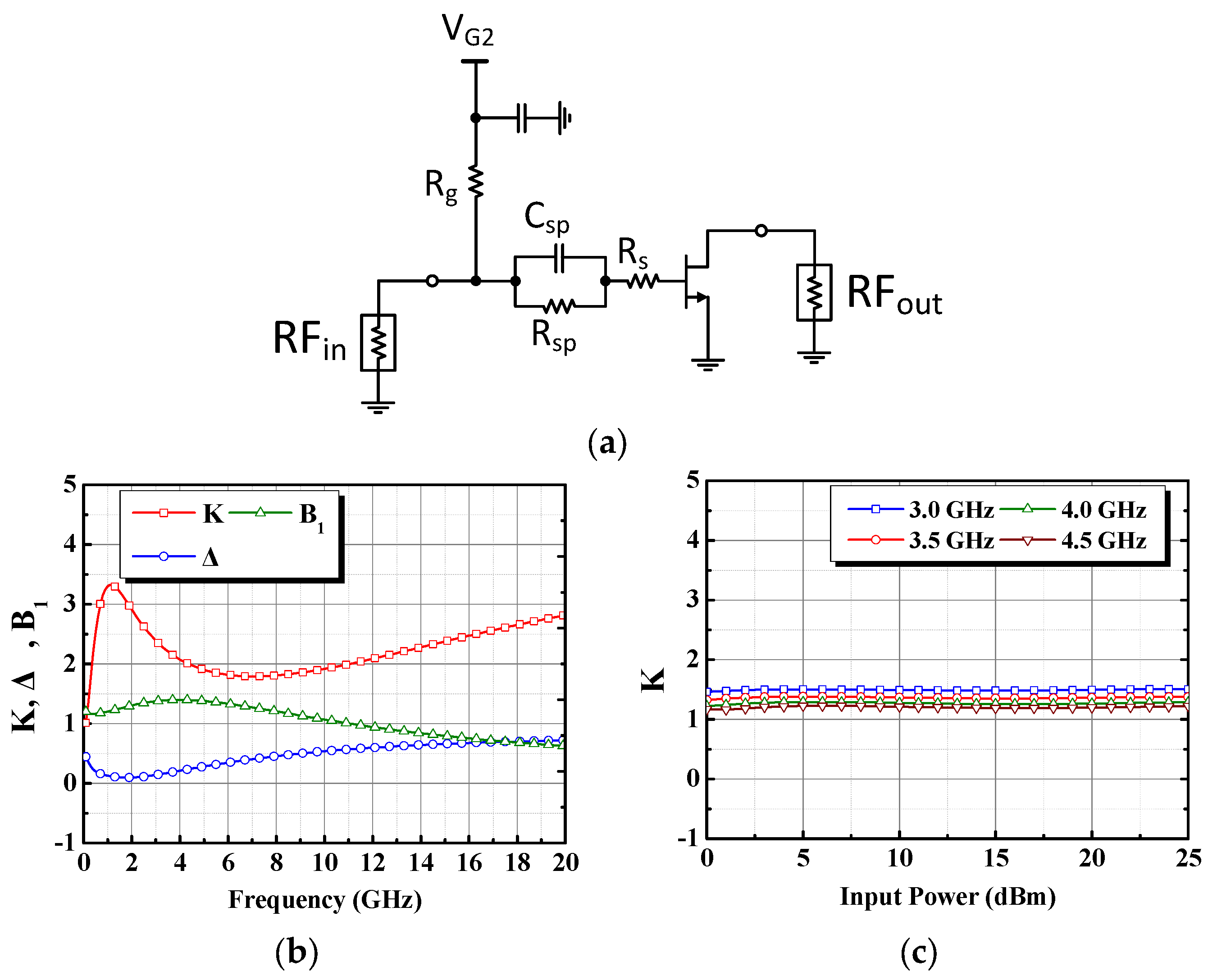
2.3. Bias and Stability Network Design

Most RF and microwave transistors are potentially unstable at both high and low frequencies. GaN HEMT could easily oscillate and burn down due to high gains and high output power. Therefore, for designing a GaN RF amplifier, it would be the first priority to keep the amplifier stable and prevent oscillation. The bias network combing the stabilized network is shown in Figure 6a. The bias network is designed using the 795 Ω gate resistor Rg with the total bypass capacitance of 16 pF. The stabilized network is designed using a 7 Ω resistor Rs and a parallel RC network, a 72.4 Ω resistor Rsp and a 2 pF capacitor Csp. Later in the layout phase, the capacitor Csp would be separated into two for layout symmetry. The parallel RC network, Rsp and Csp, is tuned for in-band stability. The parallel RC network could keep the amplifier circuit stable and does not overly degrade the gains in operation bands. The bias resistor Rg is used for low-band stability. The simulated Rollet’s stability factor (K), Δ and stability measure (B1) are shown in Figure 6b. The necessary and sufficient conditions for unconditional stability are K > 1, |Δ| < 1, and B1 > 0 [25]. In Figure 6b, the unconditionally stable conditions are fully met at both high and low frequencies. Thus, the small-signal stability was assured. The series resistor Rs is used for large-signal stability. The simulated large-signal stability factor K is shown in Figure 6c. The input power is swept from 0 to 25 dBm, and the K > 1 requirements are well-fit at 3.0–4.5 GHz. Hence, the large-signal stability was also assured.

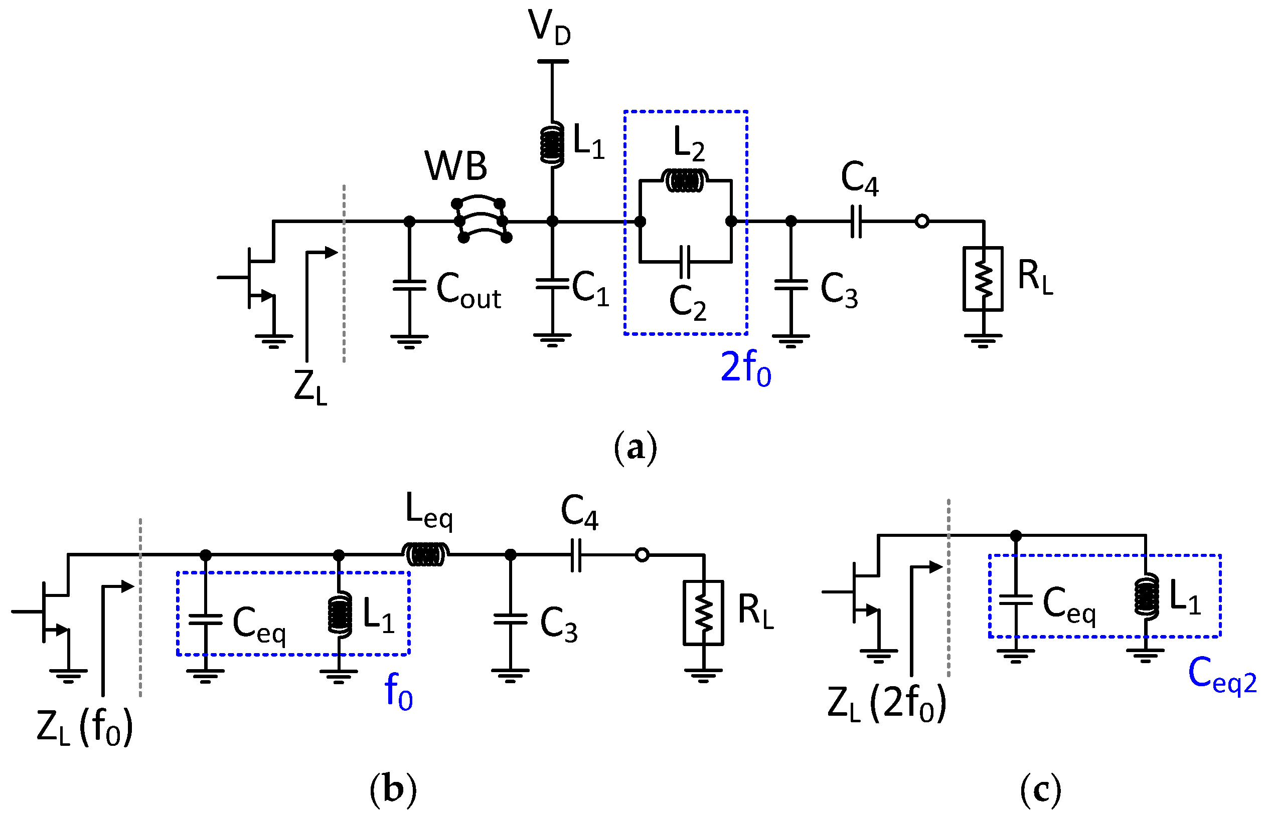
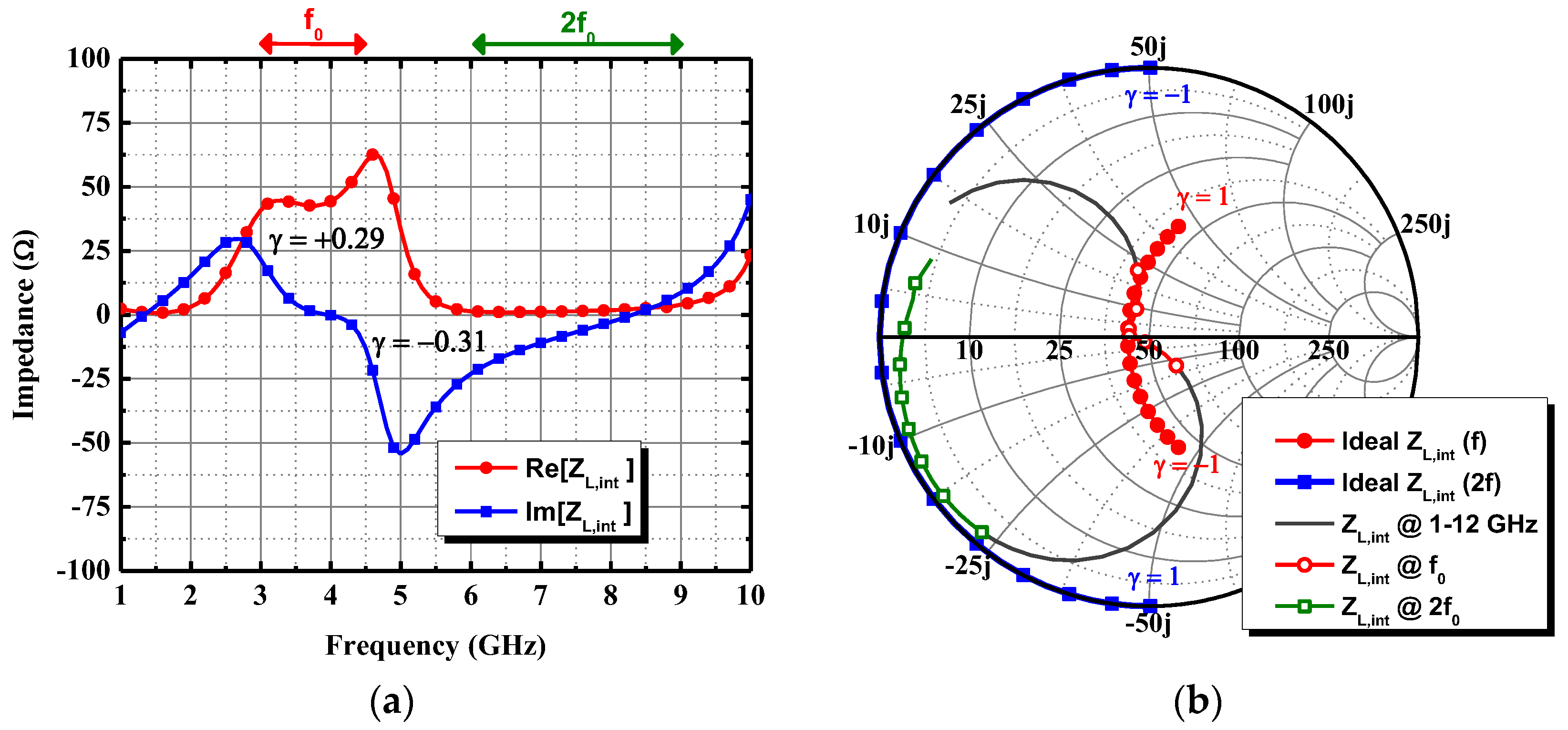
2.4. Class-J Output Matching Network

The continuous Class-J mode specifies the optimum load impedances at the fundamental frequency and the second harmonic frequency, as follows [26,27].
Z L f 0 = 1 + j γ R o p t
Z L 2 f 0 = j 3 π / 8 γ R o p t
For the third- and higher-order harmonics, the optimal load impedances are considered to be short circuits in the continuous Class-J mode. The term Ropt represents the optimal load resistance of the transistor. The parameter γ is derived from the voltage and current waveform and is utilized to determine the load impedance (ZL). If the value of γ falls within the range of −1 to 1, it indicates that the continuous Class-J mode can be sustained. Consequently, it becomes possible to attain output power, efficiency, and bandwidth.
Figure 7a illustrates the OMN design, in which RL represents the load impedance of 50 Ω. The capacitor Cout represents the transistor’s drain–source parasitic capacitance. The resonant circuit L2//C2 is designed to function as an open circuit at the second harmonic frequency. Additionally, the capacitor C4 serves as a DC block in the circuit.
Figure 7b displays the OMN equivalent circuit at the fundamental frequency. In order to compensate for the presence of wire bond (WB) between GaN and GaAs IPD chips, the capacitor C1 is designed so that Cout, WB, and C2 form a combination to achieve an equivalent capacitive reactance, denoted as Ceq. Subsequently, the inductor L1 is designed to resonate with the Ceq at the fundamental frequency. Therefore, the OMN functions as an L-type impedance matching network, utilizing the combination of Leq and C3 to convert the load impedance RL to Ropt.
Figure 7c depicts the equivalent circuit of the OMN at the second harmonic frequency. The resonant circuit L2//C2 functions as an open circuit at the second harmonic frequency. The reactance of L1 increases as the frequency rises. Thus, the L1//Ceq is designed to be equivalent to a capacitor, denoted as Ceq2. As a result, the load impedance ZL(2f0) could achieve purely imaginary impedance as described in the Equation (2). The capacitor C3 plays a crucial role in reducing the load RL and eliminating the resistances. This enables the resonant circuit L2//C2 to behave more like an open circuit. Consequently, it becomes easier to achieve a small and purely imaginary impedance, which is advantageous compared to the approach described in [28].
The optimum load of 40 Ω is obtained through load-pull simulation along with the equivalent output capacitance (Cout) of 974 fF. Figure 8a illustrates the frequency response of the designed OMN in a rectangular plot, while Figure 8b represents the same response in a Smith chart. At the fundamental frequency, the real part of output impedance is approximately 42 Ω and the parameter γ ranges from −0.31 to 0.29. At the second harmonic frequency, the real part of output impedance approaches zero, resulting in a purely imaginary impedance. The simulated result validates that the power amplifier operates in the continuous Class-J mode.

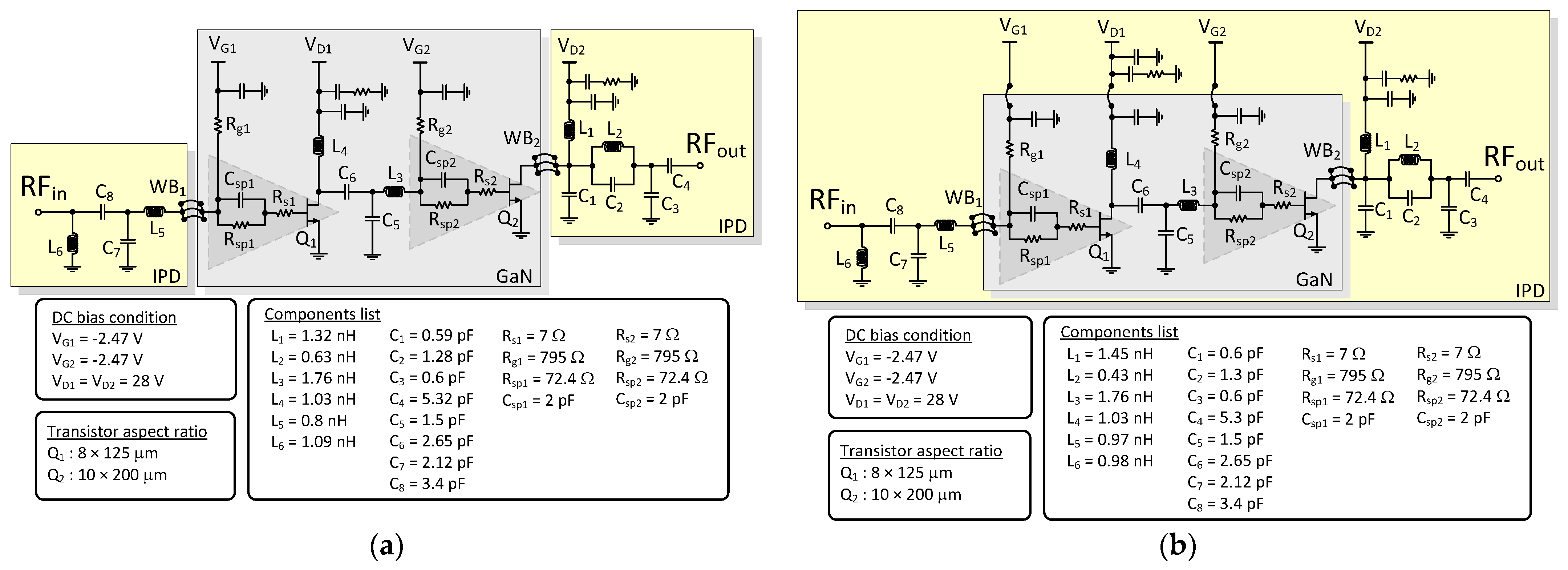
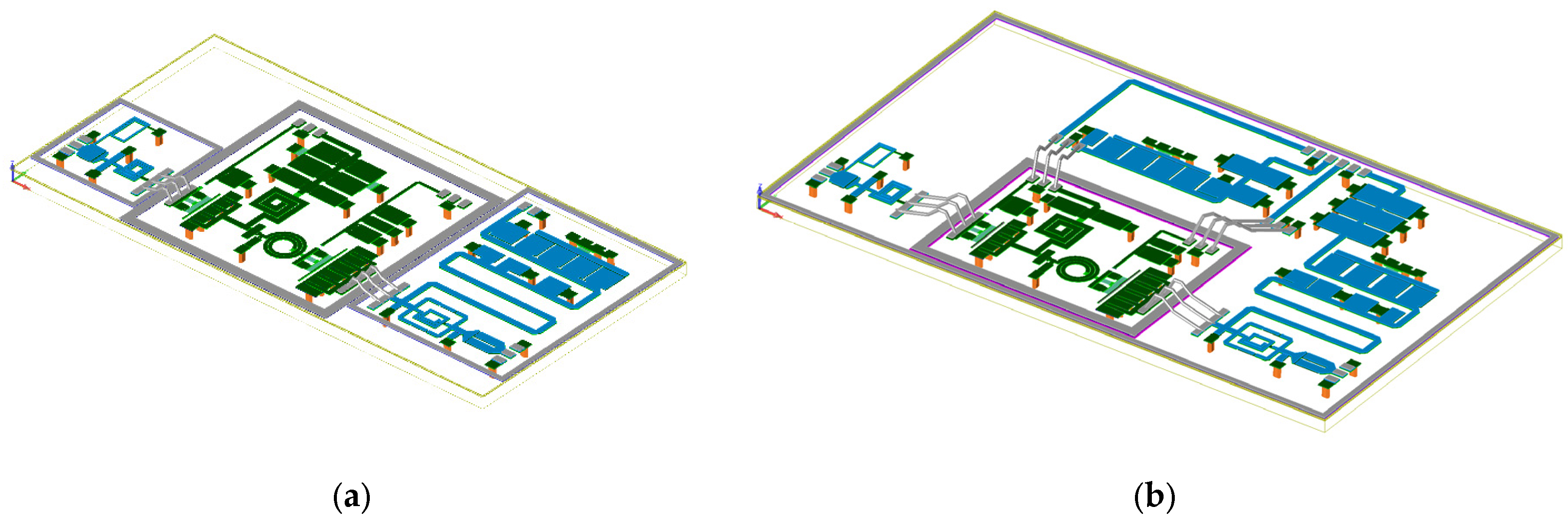
2.5. Schematics, Assemblies, and 3D Views

Figure 9a,b displays the schematics and components lists of the proposed continuous Class-J mode quasi-MMIC PAs that utilize GaN and GaAs IPD technology. In Figure 9a, the design is based on a split CoB wire-bond assembly. On the other hand, Figure 9b represents a stack CoB wire-bond assembly design. In these PA designs, the transistors’ gate widths are designed as 1000 (8 × 125) µm for the driver stage (Q1) and 2000 (10 × 200) µm for the output stage (Q2). The PAs are configured with a 1:2 gate periphery driving ratio, which guarantees sufficient driving to saturate the output stage. Both stages are biased at deep class AB. The resistors (Rsp1 and Rsp2) of the stability networks are divided equally by two resistors to achieve a balanced layout configuration with a symmetrical signal path. The input matching network and interstage matching network utilize a band-pass matching technique to enhance the overall bandwidth of the PAs.
Figure 10a,b presents the assemblies and 3D views of the quasi-MMIC PAs. Figure 10a depicts the split CoB wire-bond assembly design, while Figure 10b shows the stack CoB wire-bond assembly design. These figures provide a visual representation of the physical layout and arrangement of the components in the PAs.

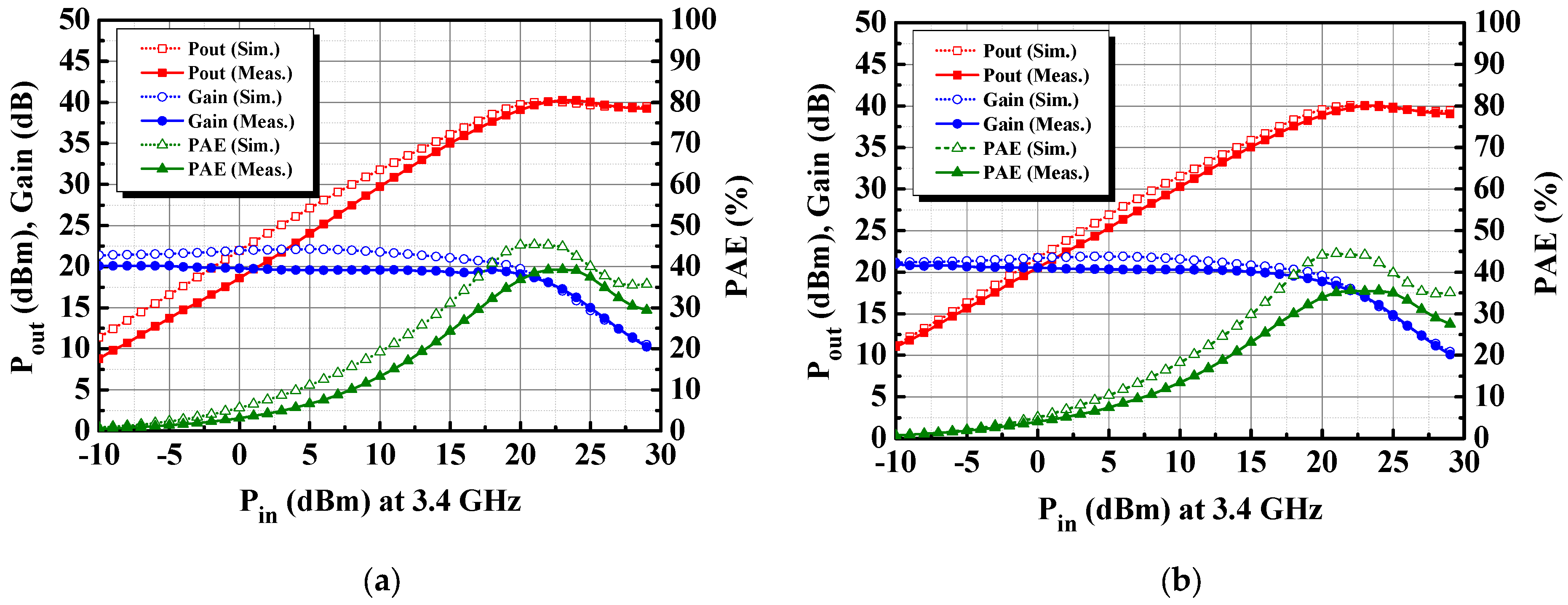
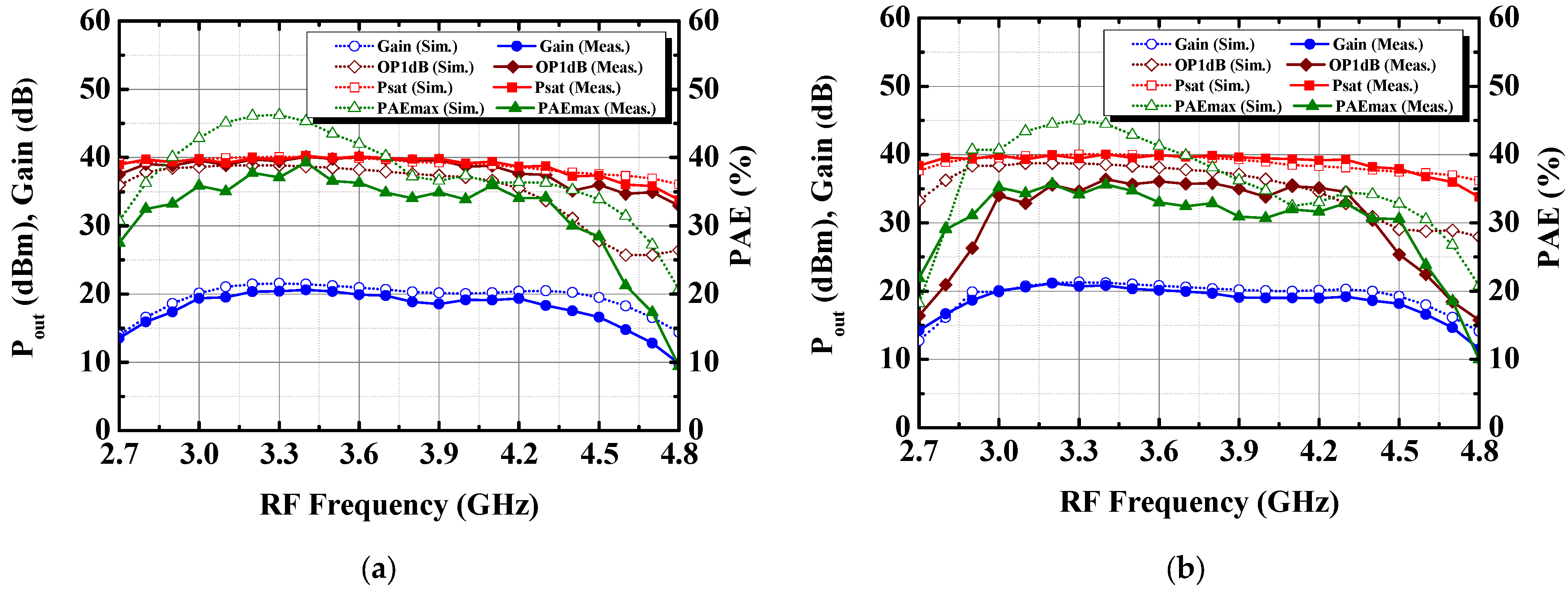
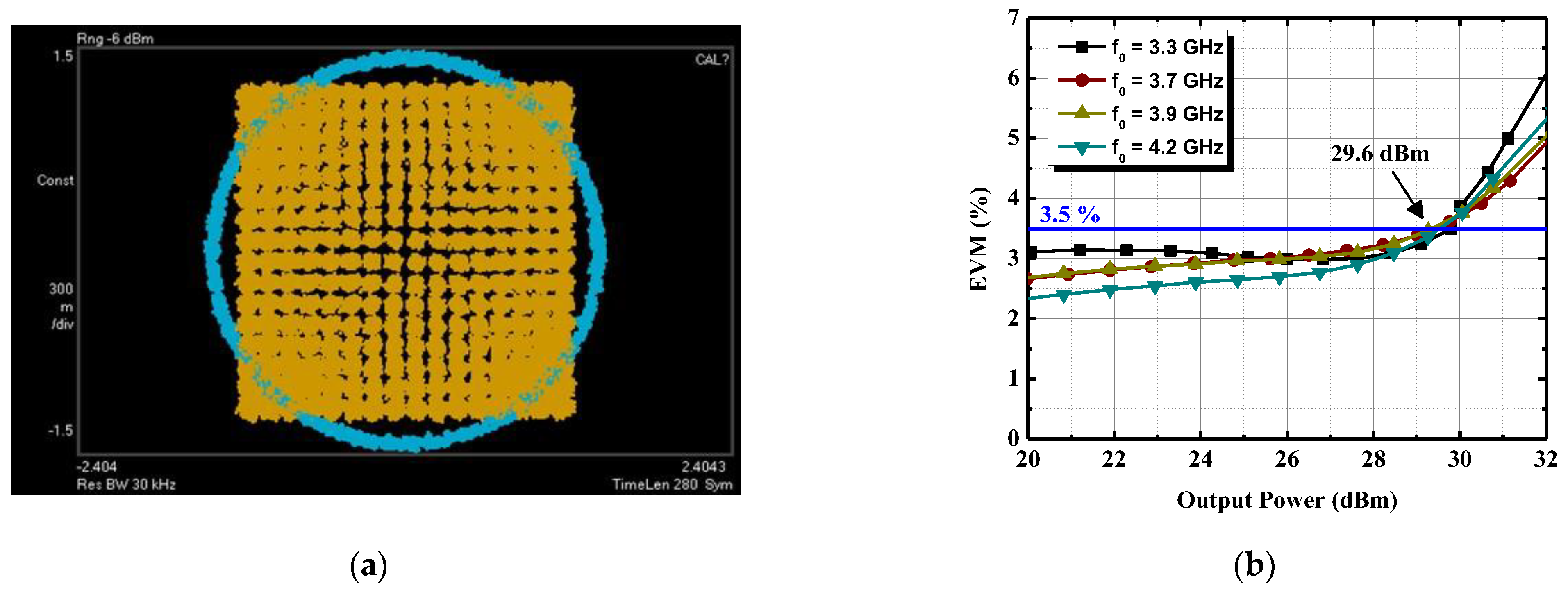
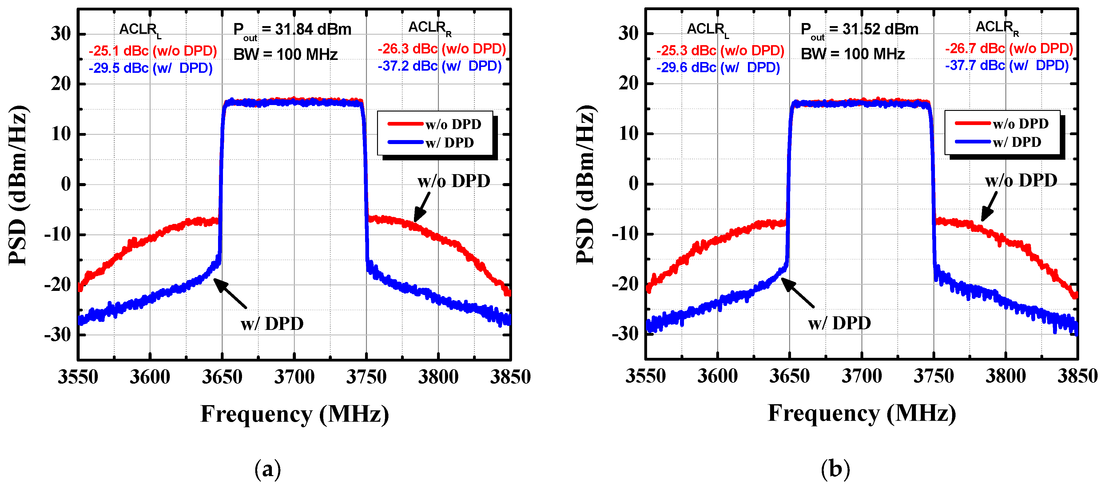
3. Experimental Results and Discussion

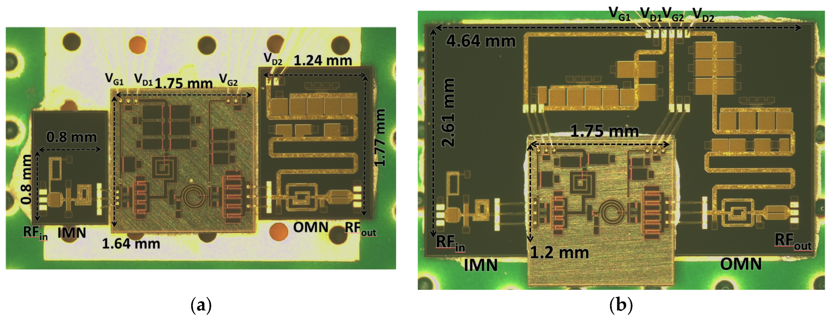
3.1. Chip Photographs and Assemblies

The photographs of the fabricated quasi-MMIC PAs are displayed in Figure 11a,b. These chips are adhered to a four-layer PCB using ABLEBOND 84-1LMISR4 conductive adhesive. Among them, the stack design GaN chip is mounted on top of the GaAs IPD. To prevent the conductive adhesive from overflowing onto the PCB pads, the bond wire in the stack design is slightly longer compared to the split design. In the split design, the GaN chip area, excluding the cutting street, was 2.87 mm2 (1.75 × 1.64 mm). The sizes of the GaAs IPD chips for input matching network (IMN) and OMN were 0.64 mm2 and 2.19 mm2 (0.8 × 0.8 mm and 1.24 × 1.77 mm), respectively. On the other hand, in the stack design, the GaN chip area, excluding the cutting street, was 2.1 mm2 (1.75 × 1.2 mm). As for the GaAs IPD chip in this configuration, the area was 12.11 mm2 (4.64 × 2.61 mm). Despite the fact that the stack design utilizes a larger area of GaAs IPD chips compared to the split design, it consumes less GaN chip area while providing greater potential for additional system integration. With the stack design, there are increased possibilities for integrating the remaining transceiver components directly on the GaAs chip using chip-on-chip (CoC) technology, ultimately enabling the integration of a system-in-package (SiP).
As mentioned in Section 2.1, heat sinks are employed on the backside of the PCB to enhance heat dissipation from the output-stage GaN transistors. Additionally, off-chip bypass capacitors are soldered onto the PCB to improve the stability of the low-frequency band. These measures ensure that the power amplifiers operate within safe temperature limits and maintain reliable operation while minimizing potential stability issues.
The measurement signal input and output were performed using RF wafer probing, while the bias currents were supplied by bond wires through PCB traces. It is noted that the current-carrying capacity of a 1.0 mil diameter gold bond wire is 0.5 A. Given that the simulated drain current of the output-stage transistor is 0.57 A, double bonds are employed from the drain DC pad to the PCB pad to ensure sufficient current-handling capacity.

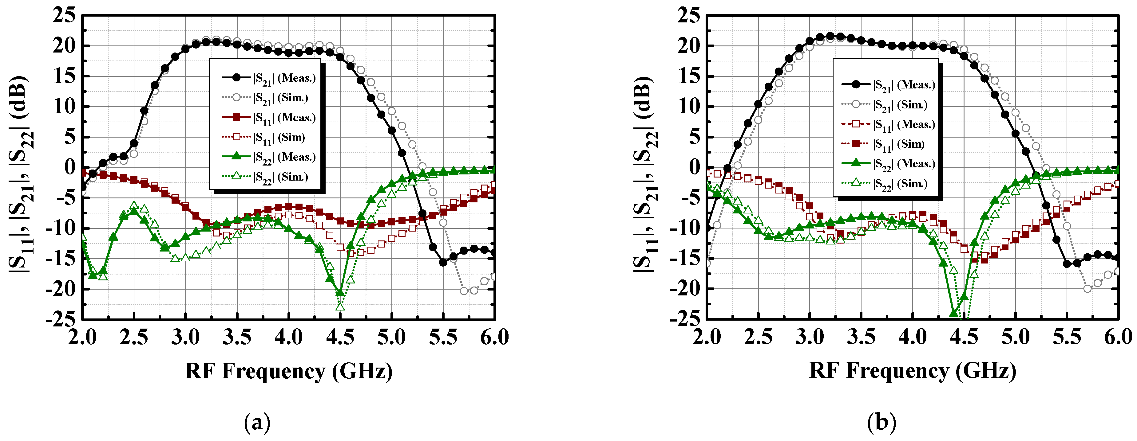
3.2. Small-Signal and Large-Signal Characterizations

Figure 12a,b presents the S-parameters observed under biased currents of ID1 = 16 mA and ID2 = 21 mA and supply voltages of VD1 = VD2 = 28 V. The split CoB wire-bond assembly PA demonstrated a small-signal gain of 21.7 dB and a 3 dB bandwidth ranging from 2.85 to 4.48 GHz, resulting in a 44.5% fractional bandwidth. Similarly, the stack CoB wire-bond assembly PA achieved a small-signal gain of 21.6 dB and a 3 dB bandwidth ranging from 2.84 to 4.47 GHz, leading to a 44.6% fractional bandwidth. Analytical evaluations indicated favorable agreement between the simulated and measured results. These findings suggest that the designed PAs perform well and exhibit good agreement between the simulated performance and the measured performance.
The large-signal power performances were evaluated using pulsed RF measurements conducted with PXA-N5247B to avoid excessive temperature rise and potential damage to the GaN chips. The measurements involved a pulse width of 100 μs and a duty cycle of 10%. Figure 13a,b presents the power performances at 3.4 GHz. The split CoB wire-bond assembly PA exhibited a Psat value of 40.3 dBm (10.7 W), an OP1dB value of 36.4 dBm, and a peak PAE of 39.3%. The stack CoB wire-bond assembly PA exhibited a Psat value of 40 dBm (10 W), an OP1dB value of 36.4 dBm, and a peak PAE of 35.6%.
Figure 14a,b illustrates plots showing power versus frequency, both measured and simulated, for the designed PAs. For the split CoB wire-bond assembly PA, the measured Psat value exceeded 37.4 dBm (equivalent to 5.5 W) within the frequency range of 2.7 to 4.5 GHz, and the peak power-added efficiency (PAE) was above 27.5%. Additionally, with a Psat value of 40.3 dBm, the 3 dB power bandwidth covered the range from 2.7 to 4.5 GHz, resulting in a 42% power fractional bandwidth (PFBW). On the other hand, for the stack CoB wire-bond assembly PA, the measured Psat value surpassed 37.9 dBm (6.2 W) within the 2.7 to 4.5 GHz frequency range, and the peak PAE was higher than 22%. The Psat value of 40 dBm indicated a 3 dB power bandwidth spanning from 2.7 to 4.5 GHz, providing a 50% PFBW. These measured power frequency responses of the designed PAs are well-suited for 5G NR FR1 n77 and n78 bands.

3.3. Modulation Signal Characterizations

The modulation signal measurement was carried out using specific test equipment, including a Mini-Circuits ZVE-3W-83+ pre-amplifier, Keysight AWG M8190A, PSG E8267D, and UXA N9041B devices. The modulation signal used was a 5G New Radio (NR) Frequency Range 1 (FR1) signal with a bandwidth of 100 MHz, utilizing 256-QAM modulation with a coding rate of 3/4.
Figure 15a,b displays plots representing the measured constellation and error vector magnitude (EVM) for both the split and stack design power amplifiers (PAs) against various average output power values. The split CoB wire-bond assembly PA achieved an average output power of 29.6 dBm while meeting the EVM requirement of 3.5%. Similarly, the stack CoB wire-bond assembly PA yielded an average output power of 28.3 dBm under the same EVM requirement of 3.5%. These results indicate that both the split and stack design PAs are suitable for 5G NR operation as they meet the EVM and output power specifications for reliable and efficient communication in the 5G NR FR1 n77 and n78 bands.
The results of the DUT power spectrum density (PSD) and adjacent channel leakage power ratio (ACLR) measurements with a 5G NR FR1 100 MHz 256-QAM signal are displayed in Figure 16. With the implementation of digital predistortion (DPD), both the split design PA and the stack design PA were able to meet the stringent −30 dBc (decibels relative to the carrier) user equipment ACLR requirement for the n77 and n78 frequency bands. The split PA achieved this performance with an average output power (Pout) of 31.8 dBm, while the stack PA achieved it with a slightly lower average Pout of 31.5 dBm. The implementation of DPD also improved the EVM results. Both designs fulfilled the EVM requirement of 3.5% under the power levels.
By using DPD, these power amplifiers were able to effectively mitigate distortions and non-linearities, ensuring that the transmitted signals meet the required standards for adjacent channel emissions, which is critical for maintaining a high-quality and interference-free communication in the 5G NR n77 and n78 bands.

4. Discussion

Table 1 provides a comparison of various S/C-band GaN power amplifiers proposed in the literature [29,30,31]. The PAEpeak denotes the maximum PAE achieved at saturated output power. We have included [28] in the table due to the resemblance of its continuous mode design to that of this study. It is noteworthy to assess the performance against our CoB wire-bond assembly outcomes. Despite [28] being a one-stage design, our split design retains a smaller GaN chip area compared to [28], while still maintaining commendable output performance. Although our work entails a two-stage PA design, we have included [29,30] for comparison purposes. Furthermore, the GaN chip areas in our designs are also smaller than those in [29,31].
The proposed quasi-MMIC PAs are designed in two stages while utilizing the minimum GaN chip area. This design approach optimizes the use of expensive GaN 0.25 μm chips, reducing costs significantly. Furthermore, considering that GaAs IPD chips cost about 1/4 of GaN 0.25 μm chips, the proposed quasi-MMIC PAs are not only highly efficient but also cost-effective.
The combination of superior performance and cost effectiveness makes the proposed PAs stand out as a compelling solution. They provide excellent power efficiency, output power, bandwidth, and power gain, making them well-suited for S/C-band applications. Overall, the proposed PAs demonstrate a well-balanced approach, maintaining good performance while also considering cost considerations, which makes them a highly competitive choice compared to other alternatives discussed in the literature.

5. Conclusions

In the present study, two quasi-MMIC two-stage PAs were developed for the 5G NR n77 and n78 bands using WINTM Semiconductors’ 0.25 μm GaN/SiC HEMT process and GaAs IPD process. Given thermal considerations, the CoB wire-bond assembly method was chosen, and the interconnect design was carefully executed using three bond wires with lengths of 300–400 μm. To demonstrate the concept’s potential, two assembly methods were implemented: the split and stack designs. The split design consists of GaN chips with an area of 2.87 mm2 along with GaAs IPD chips measuring 0.64 mm2 and 2.19 mm2 (excluding the cutting street). The split design was found to be the more cost-effective option. On the other hand, the stack design involves GaN chips with an area of 2.1 mm2 and GaAs IPD chips with a much larger area of 12.11 mm2. The stack design optimizes the GaN chip sizes while providing a larger GaAs IPD area. This larger GaAs IPD chip area presents the potential for integrating an SiP, enabling further development with advanced functionalities.
The continuous Class-J mode design was employed for both spilt and stack design. The CoB wire-bond assembly was carefully considered in the IMN and OMN designs. The fabricated split design PA achieved a maximum Psat value of 40.3 dBm (10.3 W), an OP1dB value of 36.4 dBm, a bandwidth of 44.5%, and a peak PAE of 39.3%. On the other hand, the stack CoB wire-bond assembly PA achieved a maximum Psat value of 40 dBm (10 W), an OP1dB value of 36.4 dBm, a bandwidth of 44.6%, and a peak PAE of 35.6%. Both the split and stack design PAs demonstrated Psat values exceeding 37.4 dBm and 37.9 dBm within the frequency range of 2.7 to 4.5 GHz. The fabricated PAs exhibited excellent in-band and out-of-band performance under a 5G NR FR1 100 MHz 256-QAM signal. The overall measurement results indicate that the proposed two continuous Class-J mode quasi-MMIC PAs can be used for 5G NR FR1 microcell applications.

Author Contributions

Conceptualization, H.-C.L. and H.-K.C.; methodology, H.-C.L.; software, H.-C.L.; validation, H.-C.L.; formal analysis, H.-C.L.; investigation, H.-C.L.; resources, H.-C.L.; data curation, H.-C.L.; writing—original draft preparation, H.-C.L.; writing—review and editing, H.-C.L.; visualization, H.-C.L.; supervision, D.-C.C. and H.-K.C.; project administration, D.-C.C. and H.-K.C.; funding acquisition, D.-C.C. and H.-K.C. All authors have read and agreed to the published version of the manuscript.

Funding

This research was funded by the Ministry of Science and Technology of Taiwan under contract number MOST 109-2221-E-008-065-MY3 and MOST 112-2218-E492-005.

Data Availability Statement

Not applicable.

Acknowledgments

The authors thank the Taiwan Semiconductor Research Institute (TSRI) and the National Chung-Shan Institute of Science & Technology (NCSIST) for their support with chip fabrication and measurement.

Conflicts of Interest

The authors declare no conflict of interest.

References

  1. Mayeda, J.C.; Lie, D.Y.C.; Lopez, J. A high efficiency fully-monolithic 2-stage C-band GaN power amplifier for 5G microcell applications. In Proceedings of the Texas Symposium on Wireless and Microwave Circuits and Systems (WMCS), Waco, TX, USA, 5–6 April 2018. [Google Scholar]
  2. Qi, T.; He, S. Power Up Potential Power Amplifier Technologies for 5G Applications. IEEE Microw. Mag. 2019, 20, 89–101. [Google Scholar] [CrossRef]
  3. Ahn, H.; Back, S.; Nam, I.; An, D.; Lee, J.; Jeong, M.; Kim, B.E.; Lee, Y.T.; Kim, H.T.; Ho, Y.C.; et al. A Fully Integrated −32-dB EVM Broadband 802.11abgn/ac PA With an External PA Driver in WLP 40-nm CMOS. IEEE Trans. Microw. Theory Tech. 2019, 67, 1870–1882. [Google Scholar] [CrossRef]
  4. Wang, Z.; Hu, S.; Gu, L.; Lin, L. Review of Ka-Band Power Amplifier. Electronics 2022, 11, 942. [Google Scholar] [CrossRef]
  5. Pengelly, R.S.; Wood, S.M.; Milligan, J.W.; Sheppard, S.T.; Pribble, W.L. A Review of GaN on SiC High Electron-Mobility Power Transistors and MMICs. IEEE Trans. Microw. Theory Tech. 2012, 60, 1764–1783. [Google Scholar] [CrossRef]
  6. Quaglia, R.; Camarchia, V.; Pirola, M.; Rubio, J.J.M.; Ghione, G. Linear GaN MMIC Combined Power Amplifiers for 7-GHz Microwave Backhaul. IEEE Trans. Microw. Theory Tech. 2014, 62, 2700–2710. [Google Scholar] [CrossRef]
  7. Cao, T.; Liu, Y.; Chen, W.; Yang, C.; Zhou, J. Analytical Design Solution for Optimal Matching of Hybrid Continuous Mode Power Amplifiers Suitable for a High-Efficiency Envelope Tracking Operation. Electronics 2019, 8, 621. [Google Scholar] [CrossRef]
  8. Ghisotti, S.; Pisa, S.; Colantonio, P. S Band Hybrid Power Amplifier in GaN Technology with Input/Output Multi Harmonic Tuned Terminations. Electronics 2021, 10, 2318. [Google Scholar] [CrossRef]
  9. Chen, X.; Wu, Y.; Wang, W. Dual-Band, Dual-Output Power Amplifier Using Simplified Three-Port, Frequency-Dividing Matching Network. Electronics 2022, 11, 144. [Google Scholar] [CrossRef]
  10. Gustafsson, D.; Andersson, K.; Leidenhed, A.; Malmstrom, M.; Rhodin, A.; Wegeland, T. A packaged hybrid doherty PA for microwave links. In Proceedings of the European Microwave Conference (EuMC), London, UK, 4–6 October 2016. [Google Scholar]
  11. Ayad, M.; Byk, E.; Neveux, G.; Camiade, M.; Barataud, D. Single and dual input packaged 5.5–6.5GHz, 20W, Quasi-MMIC GaN-HEMT Doherty Power Amplifier. In Proceedings of the IEEE MTT-S International Microwave Symposium (IMS), Honololu, HI, USA, 4–9 June 2017. [Google Scholar]
  12. Quaglia, R.; Greene, M.D.; Poulton, M.J.; Cripps, S.C. Design and characterization of a 1.7–2.7 GHz quasi-MMIC Doherty power amplifier. In Proceedings of the IEEE MTT-S International Microwave Symposium (IMS), Honololu, HI, USA, 4–9 June 2017. [Google Scholar]
  13. Quaglia, R.; Greene, M.D.; Poulton, M.J.; Cripps, S.C. A 1.8–3.2-GHz Doherty Power Amplifier in Quasi-MMIC Technology. IEEE Microw. Wirel. Compon. Lett. 2019, 29, 345–347. [Google Scholar] [CrossRef]
  14. Liu, R.-J.; Zhu, X.-W.; Xia, J.; Chen, P.; Yu, C.; Zhang, L.; Chen, Z.-Y. A 30-W GaN Quasi-MMIC Doherty Power Amplifier Based on All-Distributed Inductors Load Network. In Proceedings of the 2021 51st European Microwave Conference (EuMC), London, UK, 4–6 April 2022. [Google Scholar]
  15. Cao, Y.; Zhu, X.-W.; Liu, R.-J.; Dong, Q. Design of an S-band quasi-MMIC Power Amplifier. In Proceedings of the 2021 International Conference on Microwave and Millimeter Wave Technology (ICMMT), Nanjing, China, 23–26 May 2021. [Google Scholar]
  16. Doherty, W.H. A New High Efficiency Power Amplifier for Modulated Waves. Proc. Inst. Radio Eng. 1936, 24, 1163–1182. [Google Scholar]
  17. Raab, F.H. Class-F power amplifiers with maximally flat waveforms. IEEE Trans. Microw. Theory Tech. 1997, 45, 2007–2012. [Google Scholar] [CrossRef]
  18. Cripps, S.C.; Tasker, P.J.; Clarke, A.L.; Lees, J.; Benedikt, J. On the Continuity of High Efficiency Modes in Linear RF Power Amplifiers. IEEE Microw. Wirel. Compon. Lett. 2009, 19, 665–667. [Google Scholar] [CrossRef]
  19. Carrubba, V.; Clarke, A.L.; Akmal, M.; Lees, J.; Benedikt, J.; Tasker, P.J.; Cripps, S.C. The Continuous Class-F Mode Power Amplifier. In Proceedings of the 40th European Microwave Conference, Paris, France, 28–30 September 2010. [Google Scholar]
  20. Tasker, P.J.; Carrubba, V.; Wright, P.; Lees, J.; Benedikt, J.; Cripps, S. Wideband PA Design: The “Continuous” Mode of Operation. In Proceedings of the 2012 IEEE Compound Semiconductor Integrated Circuit Symposium (CSICS), La Jolla, CA, USA, 14–17 October 2012. [Google Scholar]
  21. Li, C.-H.; Ko, C.-L.; Kuo, C.-N.; Kuo, M.-C.; Chang, D.-C. A Low-Cost DC-to-84-GHz Broadband Bondwire Interconnect for SoP Heterogeneous System Integration. IEEE Trans. Microw. Theory Tech. 2013, 61, 4345–4352. [Google Scholar] [CrossRef]
  22. Chan, C.-H.; Chou, C.-C.; Chuang, H.-R. Integrated Packaging Design of Low-Cost Bondwire Interconnection for 60-GHz CMOS Vital-Signs Radar Sensor Chip with Millimeter-Wave Planar Antenna. IEEE Trans. Compon. Packag. Manuf. Technol. 2018, 8, 177–185. [Google Scholar] [CrossRef]
  23. Umar, M.; Laabs, M.; Neumann, N.; Plettemeier, D. Bondwire Model and Compensation Network for 60 GHz Chip-to-PCB Interconnects. IEEE Antennas Wirel. Propag. Lett. 2021, 20, 2196–2200. [Google Scholar] [CrossRef]
  24. Nunes, L.C.; Cabral, P.M.; Pedro, J.C. AM/AM and AM/PM Distortion Generation Mechanisms in Si LDMOS and GaN HEMT Based RF Power Amplifiers. IEEE Trans. Microw. Theory Tech. 2014, 62, 799–809. [Google Scholar] [CrossRef]
  25. Gonzalez, G. Microwave Transistor Amplifiers: Analysis and Design, 2nd ed.; Pearson: London, UK, 1996; pp. 240–243. [Google Scholar]
  26. Saxena, S.; Rawat, K.; Roblin, P. Continuous Class-B/J Power Amplifier Using a Nonlinear Embedding Technique. IEEE Trans. Circuits Syst. II Exp. Briefs 2017, 64, 837–841. [Google Scholar] [CrossRef]
  27. Alizadeh, A.; Hassanzadehyamchi, S.; Medi, A. Integrated Output Matching Networks for Class–J/J−1 Power Amplifiers. IEEE Trans. Circuits Syst. I Reg. Pap. 2019, 66, 2921–2934. [Google Scholar] [CrossRef]
  28. Nikandish, G.; Staszewski, R.B.; Zhu, A. Design of Highly Linear Broadband Continuous Mode GaN MMIC Power Amplifiers for 5G. IEEE Access 2019, 7, 57138–57150. [Google Scholar] [CrossRef]
  29. Florian, C.; Cignani, R.; Niessen, D.; Santarelli, A. A C-BAND AlGaN-GaN MMIC HPA for SAR. IEEE Microw. Wirel. Compon. Lett. 2012, 22, 471–473. [Google Scholar] [CrossRef]
  30. May, S.; Maassen, D.; Rautschke, F.; Boeck, G. Two stage 4–8 GHz, 5 W GaN-HEMT amplifier. In Proceedings of the 2017 47th European Microwave Conference (EuMC), Nuremberg, Germany, 10–12 October 2017. [Google Scholar]
  31. Zhao, B.; Sanabria, C.; Hon, T. A 2-Stage S-Band 2W CW GaN MMIC Power Amplifier in an Overmold QFN Package. In Proceedings of the 2022 IEEE Texas Symposium on Wireless and Microwave Circuits and Systems (WMCS), Waco, TX, USA, 19–20 April 2022. [Google Scholar]
Figure 1. The candidates for assembly method: (a) flip-chip assembly; (b) split CoB wire-bond assembly; and (c) stack CoB wire-bond assembly.
Electronics 12 03494 g001
Figure 2. The 3D FEM simulation settings of different quantities of 300 μm length bond wires: (a) one bond wire; (b) two bond wires; (c) three bond wires; (d) four bond wires; and (e) five bond wires.
Electronics 12 03494 g002
Figure 3. The S-parameters simulation results of 300 μm length bond wires with different quantities: (a) |S11|; (b) |S21|; and (c) |S11| (Smith chart).
Electronics 12 03494 g003
Figure 4. The S-parameters simulation results of 400 μm length bond wires with different quantities: (a) |S11|; (b) |S21|; and (c) |S11| (Smith chart).
Electronics 12 03494 g004
Figure 5. The simulated large-signal output performances of the 10 × 200 µm transistor at 3.7 GHz: (a) power and PAE contours; (b) dynamic load line; (c) simulated Gm versus Pin under different bias voltages (VGS).
Electronics 12 03494 g005
Figure 6. (a) The bias and stability network; (b) Rollet’s stability factor (K), Δ and stability measure (B1); (c) large-signal K.
Electronics 12 03494 g006
Figure 7. (a) The designed OMN of the proposed quasi-MMIC Pas; (b) equivalent circuit at the fundamental frequency; (c) equivalent circuit at the second harmonic frequency.
Electronics 12 03494 g007
Figure 8. Impedance at the intrinsic plane of the output stage transistor: (a) rectangle plot; (b) Smith chart.
Electronics 12 03494 g008
Figure 9. The schematics of the proposed continuous Class-J mode quasi-MMIC PAs: (a) split CoB wire-bond assembly design; (b) stack CoB wire-bond assembly design.
Electronics 12 03494 g009
Figure 10. The 3D EM views of the proposed continuous Class-J mode quasi-MMIC PAs: (a) split CoB wire-bond assembly design; (b) stack CoB wire-bond assembly design.
Electronics 12 03494 g010
Figure 11. The assembly chip photographs of (a) split CoB wire-bond assembly design; (b) stack CoB wire-bond assembly design.
Electronics 12 03494 g011
Figure 12. The S-parameters of the proposed quasi-MMIC PAs: (a) split CoB wire-bond assembly design; (b) stack CoB wire-bond assembly design.
Electronics 12 03494 g012
Figure 13. The measured and simulated power performance at 3.4 GHz: (a) split CoB wire-bond assembly design; (b) stack CoB wire-bond assembly design.
Electronics 12 03494 g013
Figure 14. Measured and simulated power performance versus frequency: (a) split CoB wire-bond assembly design; (b) stack CoB wire-bond assembly design.
Electronics 12 03494 g014
Figure 15. Plot of the measured constellation and EVM for the split design PA: (a) constellation; (b) EVM versus output power.
Electronics 12 03494 g015
Figure 16. Plot of the measured PSD and ACLR: (a) the split CoB wire-bond assembly PA; (b) the stack CoB wire-bond assembly PA.
Electronics 12 03494 g016
Table 1. Comparison of various S/C band GaN MMIC and quasi-MMIC power amplifiers.
Reference[28][29][30][31]This Work I (Split)This Work II (Stack)
ProcessGaN 0.25 μmGaN 0.25 μmGaN DFN packaged device **GaN 0.25 μmGaN 0.25 μm GaAs IPDGaN 0.25 μm GaAs IPD
TypeOne-stage Cont. Class-BTwo-stageDiscrete two-stageTwo-stageQuasi-MMIC two-stage Cont. Class-JQuasi-MMIC two-stage cont. Class-J
Freq. (GHz)4.2–7.05.2–6.23.8–8.82.7–3.52.85–4.482.84–4.47
BW (%)5017.579.425.844.544.6
Gain (dB)12.4201719.321.721.6
Psat (dBm)36.44337.734.640.340.0
PAEpeak (%) *49413856.639.336.5
Chip Size (mm2)2.1615.75NA3.552.87 (GaN) 2.83 (GaAs)2.1 (GaN) 12.11 (GaAs)
* PAE @ saturated output power. ** Wolfspeed CGHV1F006S.
Disclaimer/Publisher’s Note: The statements, opinions and data contained in all publications are solely those of the individual author(s) and contributor(s) and not of MDPI and/or the editor(s). MDPI and/or the editor(s) disclaim responsibility for any injury to people or property resulting from any ideas, methods, instructions or products referred to in the content.

