1. Introduction
The 5th generation (5G) mobile network currently offers both the sub-6 GHz frequency range 1 (FR1) band and the millimeter-wave (mm-Wave) frequency Range 2 (FR2) band of 24.25–52.6 GHz to achieve up to 10 Gb/s download speeds for enhanced mobile broadband (eMBB) and other applications [
1]. For mm-Wave power amplifiers (PA) designed at the higher 5G FR2 band, the trade-off in linearity vs. power-added efficiency (PAE) can become considerably more complicated, making it more difficult and increasingly expensive to construct mm-Wave 5G small cells and base stations (i.e., macrocells, microcells and picocells) [
2,
3]. For a mm-Wave RF transmitter (TX), the performance of the PA can often dominate the overall TX performance in heat dissipation,
POUT, linearity, efficiency, reliability, etc. For example, modulated input signals with high a peak-to-average power ratio (PAPR) can degrade a PA’s average PAE and linear output power,
POUT, Linear, and cause TX overheating [
4]. Therefore, a highly efficient PA design with high
POUT, Linear is crucial for 5G applications. Digital predistortion (DPD) can play a pivotal role here as it can linearize the mm-Wave PAs and significantly improve their
POUT, Linear and design margins. The effectiveness of various DPD techniques can be evaluated based on their improvement of the adjacent channel leakage power ratio (ACLR) in the PA’s output spectrum, and the modulation quality determined from constellation diagrams (i.e., error vector magnitude (EVM)) [
2]. Many DPD techniques have been reported in recent years, such as the popular look-up table (LUT)-based DPD [
5], memory polynomial DPD [
6], generalized memory polynomial DPD [
7] and high I/Q imbalance DPD [
8]. For example, the DPD model reported in [
8] relies on constructing the multi-toned signal consisting of the I (in-phase) signal whose frequency components do not correlate with the Q (quadrature) signal components. Using interleaved multi-toned signals allows a faster detection of the predistortion coefficients, and the coefficients of the I/Q model are estimated and compared until the error is zero [
8]. Another possible benefit of using multi-tone signals is that the output signals can have a high spurious free dynamic range (SFDR).
This work, however, uses a relatively simpler single-tone GMP DPD model implemented in a user-friendly National Instruments (NI) mm-Wave PA testbench and not needing external FPGAs (field programmable gate arrays) [
5]. This work applies a GMP DPD algorithm to linearize a two-stage common source (CS)/two-stack gallium nitride (GaN) monolithic mm-Wave PA designed in our lab [
9]. This GMP DPD achieves impressive performance on the broadband mm-Wave PA, compared to that of other similar mm-Wave PA studies in the literature [
6,
7,
8], as discussed in
Section 2. The DPD algorithm and the experimental mm-Wave hardware DPD testbench setup are also discussed in
Section 2.
Section 3 presents the measurement results of the PA tested using long-term Evolution (LTE) quadrature amplitude modulation (64-QAM) modulated signals of different signal bandwidths (BW) at various output power levels and frequencies. We conclude by comparing our work with that conducted on several state-of-the-art mm-Wave DPD PAs in the literature.
2. Proposed GMP DPD Algorithm and Mm-Wave Hardware Testbench Setup
The memoryless look-up table (LUT) is an effective DPD technique with which to linearize mm-Wave PAs, but it does not consider the memory effects of the PAs, which can cause significant nonlinearity, such as that reported for many GaN PAs [
10,
11,
12,
13]. Therefore, generalized memory polynomial (GMP) DPD is used in this work to linearize our mm-Wave GaN PA [
9]. In this case, the output power of the PA is not only a function of the present input signal, but is also dependent on the past input signal. The output
z(
n) from pre-distorter model (A) is a non-linear function of input
x(
n − q) for all
q > 0, and it can be written as Equation (1) [
2]:
Here,
h(
q) represents voltage kernels,
q is the memory depth, and
x(
n) is the input signal to the PA.
is the system response for
x(
n) =
0,
is the unit impulse response of the system and
is the impulse response of the quadratic component of the system [
14].
can be eliminated from Equation (1) as this is a memory polynomial. The
z(
n) is a non-linear function for all (all past inputs), and
n is number of iterations. The term
x(
n) can be represented in the form of a complex baseband as in Equation (2) [
15]:
Here,
and
is the center frequency; in most cases, we consider components that are close to
. The past input signals to the PA are included in terms of voltage kernels along with the present input signal,
x(
n), to the PA. In this manner, Equation (1) digitally compensates for PA’s memory effects and nonlinearity. The GMP algorithm is a common model from the modified Volterra series using Equation (1) [
2]. The GMP model is more sophisticated than the LUT DPD model [
5,
16,
17] is in terms of its configurations which come with a higher order and address memory effects. From
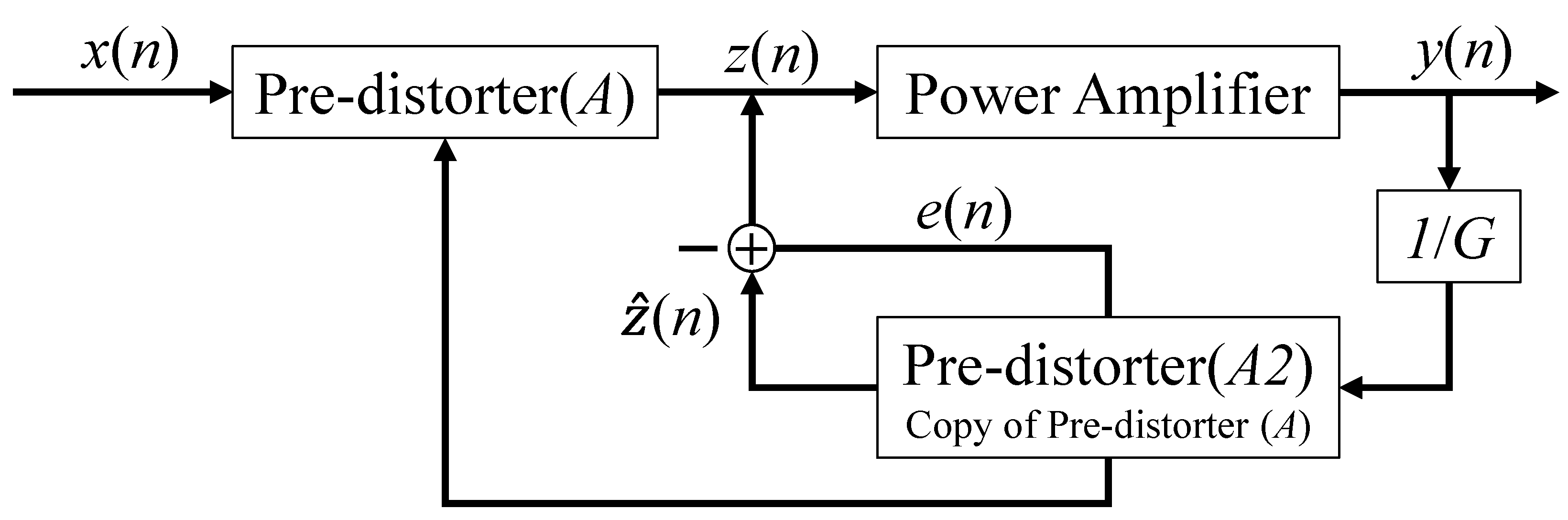
Figure 1, we can see that the input signal,
x(
n), is sent into the pre-distorter model (
A) to include the voltage kernel function,
h(
q), which accounts for the memory effects. The output signal from PA
y(
n) goes through the
1/
G block to the pre-distorter (
A2) which is
(
n). This
(
n) can be written as
y(
n)/
G. The error signal,
e(
n), is estimated per Equation (3) [
15]. Both the pre-distorters (
A and
A2) have the same DPD model, Equation (1) [
15].
The pre-distorter model (
A2) has
y(
n)/
G as its input, where
G is the PA’s gain. The output of the
A2 model is
(
n). The pre-distorter model (
A2) is a copy of the actual pre-distorter (A) which has
x(
n) as its input and
z(
n) as its output. The algorithm renders both the output
z(
n) and
(
n) of pre-distorter models (
A and
A2) until the error signal,
e(
n), is zero. As the user defines
x(
n), the data samples are known by the algorithm. The input of the pre-distorter model (
A2) is
y(
n)/
G, which is almost like the initial input signal,
x(
n). Once the signals are sent into the pre-distorter models (
A and
A2), data samples of both
(
n) and
z(
n) are gathered with the help of the NI-RFmx GUI (graphical user interface), which will be discussed later [
18]. The pre-distorter coefficients are found for both outputs of models (
A and
A2) and compared until no changes are detected (i.e.,
e(
n) is zero). If the NI-RFmx GUI detects a difference in coefficients (i.e.,
e(
n)
, the process continues by updating the polynomial order (
k) of the DPD models until the coefficients become the same (i.e.,
e(
n)
= 0). In Equation (1),
h is eliminated as it is the system response of
x(
n − q)
q =
0. From Equation (2),
z(
n) can be written in terms of the polynomial (envelope) order “
k” of the PA as shown in Equation (4) [
15]:
If
q = 0, Equation (4) turns out to be a memoryless polynomial. To consider it as a memory polynomial equation, here,
= 0
,
and
, which can be simplified into Equation (5):
From Equation (5) [
15,
19], the co-efficient from the simplified Volterra series is written as follows:
The final simplified form of the memory polynomial model equation used in the pre-distorter for the
Kth order is thus expressed in Equation (7) below:
Considering the lead and lag memory polynomial (envelope) orders in the memory polynomial function, multiple delayed versions of both positive and negative cross-term time shifts result in GMP DPD model Equation (7) [
15]. In most cases, the memory depth (
q) from Equation (7) can be set by the user. For the generalized memory polynomial function, lead and lag memory depths are defined below:
Here,
are the number of coefficients of a generalized form of an aligned envelope in the memory polynomial function,
are the number of coefficients of the lagging envelope in the memory polynomial function, and
are the number of coefficients of the leading envelope in the memory polynomial function. This makes the coefficients simple and easy to estimate from any least-squares algorithm. In most cases, Equation (8) [
2,
15] has a higher domination of odd-order linearities than of even-order linearities. As the DPD models are interested in terms that are closer to frequency
to yield satisfactory performance, the odd order linearities are chosen [
15] and it may not be necessary to implement all the delay terms in it [
15]. Here,
are the index arrays of the aligned, lagging, and leading envelopes in the memory polynomial function of Equation (8) [
2,
15].
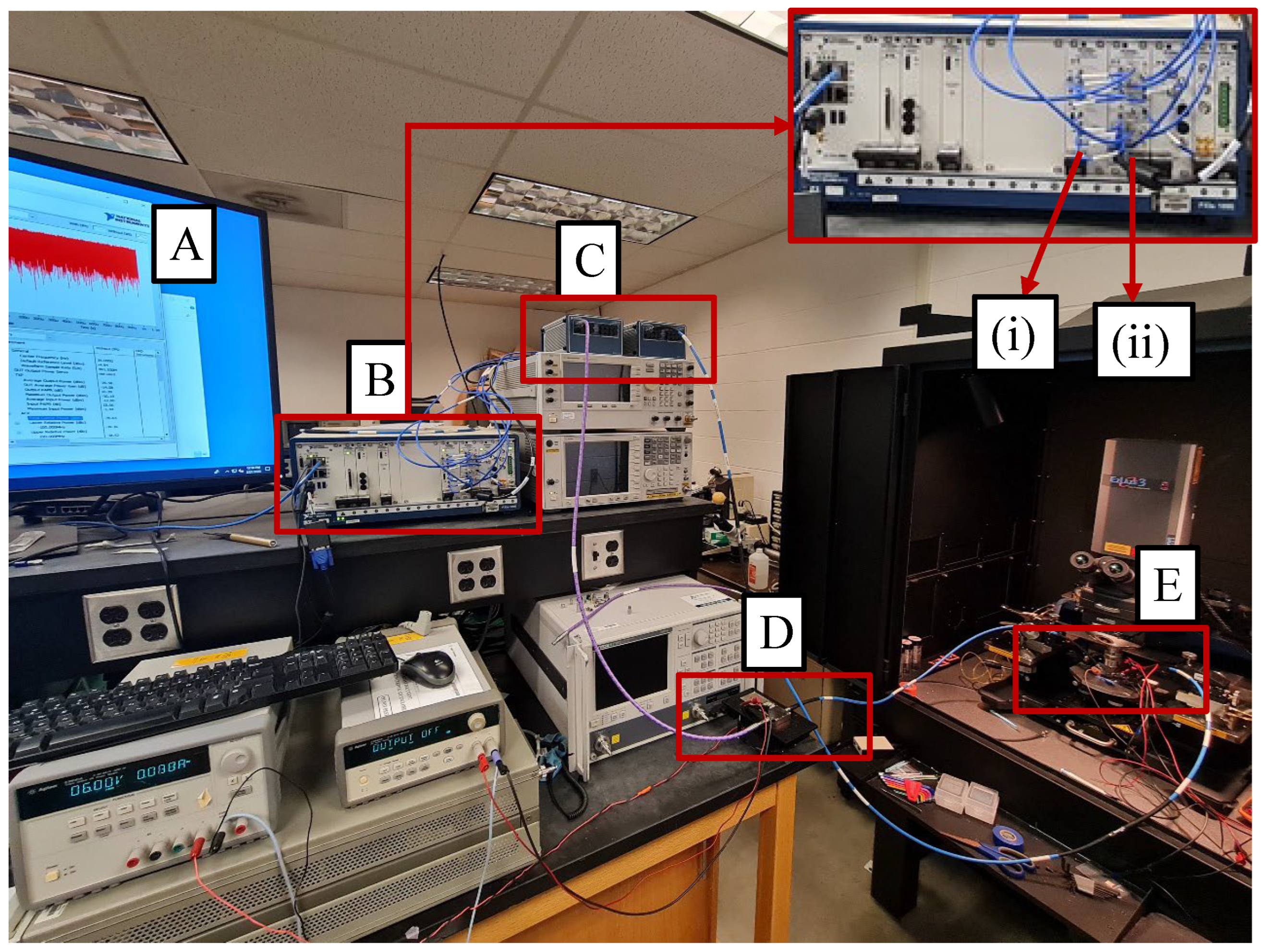
Figure 2 represents the mm-Wave PA testing setup in our lab used to linearize the PA with DPD, which consists of the I/Q signal generator PXIe-5820 [
19] (PXIe stands for the PCI express extensions for instrumentation) and the up-converter PXIe-3622 by NI (labeled “B” in
Figure 2). Baseband 64-QAM LTE input signals of four different BWs (1
20 MHz/2
20 MHz/4
20 MHz/5
20 MHz) with PAPR = 8 dB and a sampling rate of around 400 MHz–500 MHz are generated using the NI-RFmx waveform creator (labeled “A” in
Figure 2). Input signals of BW of 40 MHz/80 MHz/100 MHz are created by carrier aggregation (CA) of the baseband 64-QAM 1
20 MHz input signal using the NI-RFmx waveform creator. For example, to create the 100 MHz signal, the number of carrier offset signals is increased from 1 (1
20 MHz) to 5 (5
20 MHz). NI-RFmx is a software GUI that optimizes NI-RF instrumentations using various standard signals. NI-RFmx contains a pile of software programs that can be used to generate modulated signal waveforms using the NI-RFmx waveform creator and perform DPD using the NI-RFmx panel [
2,
19]. The generated baseband signal waveform is then sent into I/Q signal generator NI PXIe-5820. The baseband signal is converted into an intermediate frequency (IF) which is then sent to the up converter NI PXIe-3622 to be converted into the desired RF/mm-Wave signal frequency. With the help of mm radio head 5582 (labeled “C” in
Figure 2), the intended mm-Wave frequency is passed into a driver amplifier (labeled “D” in
Figure 2) to drive the two-stage CS/2-stack GaN PA (labeled “E” in
Figure 2) [
9] at the desired input signal. The broadband driver amplifier used has a BW of 18–47 GHz and it is from RF-Lambda (RFLUPA18G47GC PA with G = 37 dB and
POUT, MAX = 31 dBm) [
20]. The amplified RF/mm-Wave signal from the PA is sent back to the down converter NI PXIe-3622. The IF signals are sent back to PXIe-5820, which are passed into the lab’s PC (personal computer) for linearization. The polynomial coefficients
are estimated from the received signal into the PC, and are used to linearize/eliminate the difference vs. the source baseband signal. Settings of both the order and depth of terms such as the polynomial order, memory lag, and memory lead can be adjusted in the NI-RFmx panel [
2]. For this linearization experiment, a polynomial order (
k) of 7, memory lag (
and lead depth
of 5 and memory lag
( and lead order
of 2 are used. A lead and lag memory depth of “2” is commonly used for the GMP DPD experiments in the literature [
7,
8]. In our study, however, a lead and lag memory depth of “5” was used, which may have made our GMP DPD have better performance than those in the literature while tackling wideband signals. It took less than 30 s to perform the GMP DPD with the higher depths in our work. The GMP DPD used in this paper was also applied in a very user-friendly NI testbench.
When the user creates a baseband waveform with the help of the NI-RFmx waveform creator based on the specification, the NI-RFmx panel saves the reference waveform configurations to compare with the received baseband waveform after amplification. Both the waveforms are loaded into LabVIEW using NI-RFmx. Then, both waveforms undergo the mathematical Equation (8) [
15] to derive the polynomial coefficients
as all other factors are either given by the user or derived from the waveforms. Here,
is a transpose column vector matrix as shown in Equation (9) [
15]:
The transposition of the column vector matrix for the polynomial coefficients is carried out as it is easier to perform vector multiplication with the
x(
n − q). Considering only the higher polynomial order is sent to LabVIEW, Equation (9) is as follows:
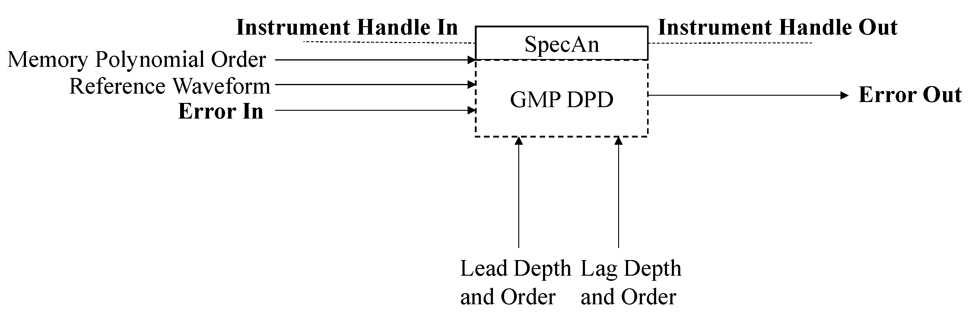
Figure 3 shows the palette of the GMP DPD operation used in the NI’s LabVIEW environment, where the orders are given by the user and the reference baseband waveform is loaded from the NI-RFmx. The user is restricted from accessing the palette as the operation happens under the hood of the NI-RFmx GUI. Initially, only the reference baseband waveform is loaded into the highlighted GMP DPD palette to obtain the reference polynomial coefficients, which are stored as the output error signals. Once we obtain the amplified signal back to NI PXIe as shown in
Figure 2, it is then sent into the “Instrument Handle In” shown in
Figure 3 as the received baseband waveform and to the highlighted GMP DPD palette to derive the polynomial coefficients
which are then compared with the input error signal, where the initial input error signal is the reference polynomial coefficients. The NI-RFmx gathers the data samples of both
(
n) and
z(
n). The difference between the coefficients is stored again as the error signal
e(
n). The process goes on until the output error signal reaches zero. In most cases, the output error signal reaches zero after two iterations (
n = 2) [
2]. Thus, the GMP DPD linearizes the PA.
3. Mm-Wave DPD Measurement Results on 4G LTE 64-QAM Modulated Signals
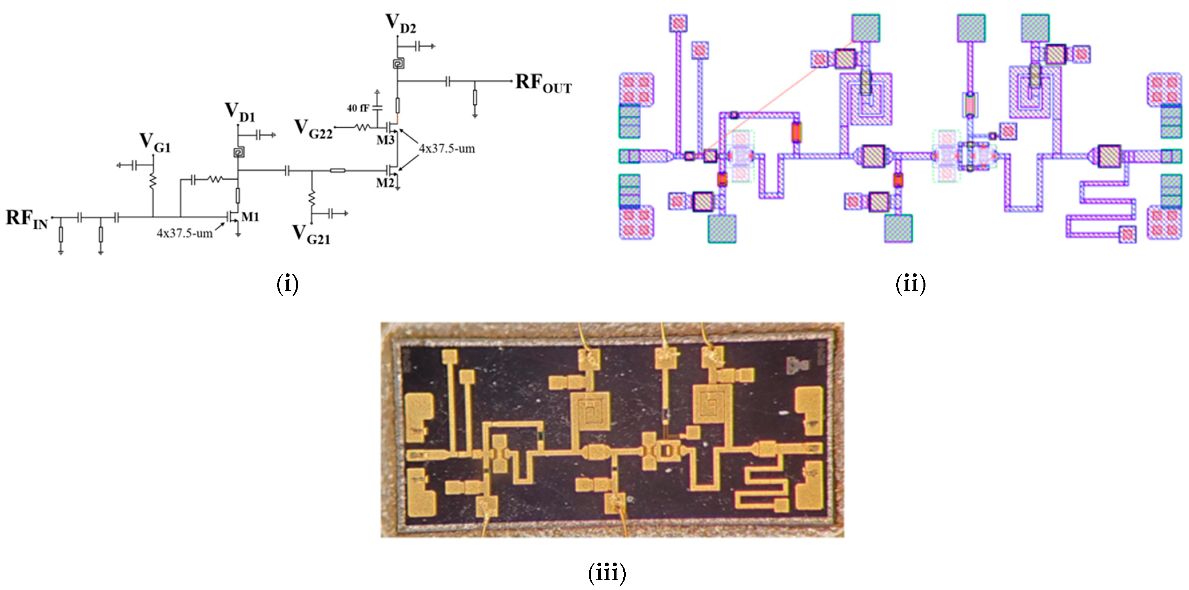
We will discuss in this section the DPD measurement results on the mm-Wave two-stage CS/two-stack GaN PA [
9]. This is a broadband two-stage CS/2-stack GaN PA with a small-signal 3 dB bandwidth of 19.9–35.1 GHz (55.3%), while its large signal
POUT, SAT 1 dB bandwidth may be significantly larger. The core die size of the PA is 1.9 mm
2 (without pads), the gain is >~20 dB, and
POUT, MAX = 22 dBm. The simplified schematics, layout and die micrograph of the PA are shown in
Figure 4. For the DPD work, to study the effects on the modulated signal bandwidth, we use 1
20 MHz, 2
20 MHz, 4
20 MHz, and 5
20 MHz LTE 64-QAM signal with PAPR = 8 dB as the input signal.
The two-stage CS/2-stack GaN PA has a CS driver first stage with negative resistive feedback that drives the two-stack second stage, which is biased at a current density of ~0.2 mA/μm. For this work, the PA is operated at drain voltages (VD1/VD2) of 6 V/12 V, and the gate voltages VG1/VG21/VG22 are 0.2 V/0.2 V/5.8 V.
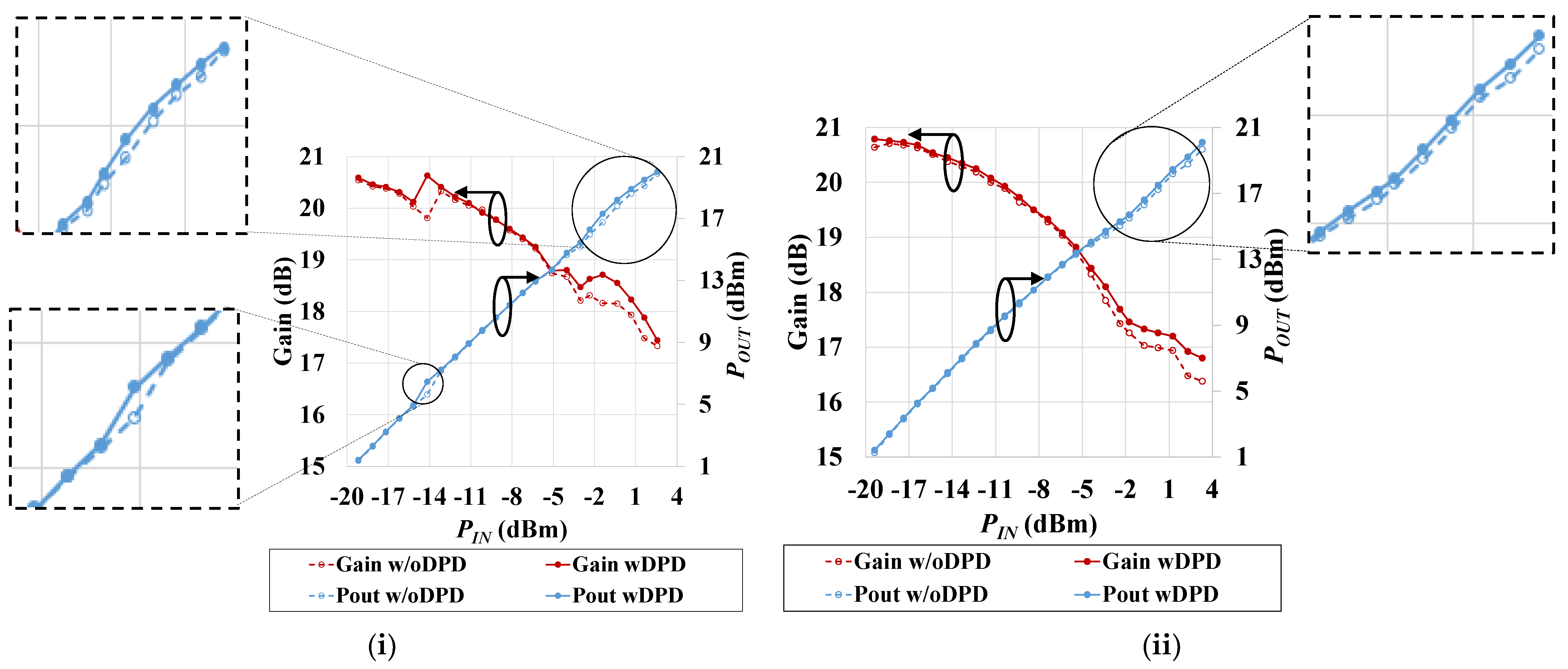
Figure 5 shows the gain and the
average POUT vs. the
average PIN measurement results of the two-stage GaN PA using the 5
20 MHz LTE 64-QAM input signal of PAPR = 8 dB. The PA has the highest gain improvement of 0.6 dB using the GMP DPD, with the
average PIN of around −1 dBm at 24 GHz. The gain at a higher
PIN improves/expands significantly after using the GMP DPD, as can be seen in the zoom-up inserts in
Figure 5. The
average POUT improvements are highlighted and zoomed into in
Figure 5, and this parameter has the best improvement at 24 GHz.
Figure 5i shows that the GMP DPD linearizes the PA even at a lower input power (
average PIN = −14 dBm) if needed. The PA has achieved a gain improvement around 0.5 dB with an
average PIN of around 2 dBm/5 dBm/7 dBm at 28 GHz/37 GHz/39 GHz using the 5
20 MHz LTE 64-QAM modulated input signal of PAPR = 8 dB.
The power-added efficiency (PAE) of the PA has the highest improvement of only around 2% when the PA is operated with a high
average POUT of around 20 dBm at 39 GHz using a 5
20 MHz LTE 64-QAM signal with PAPR = 8 dB.
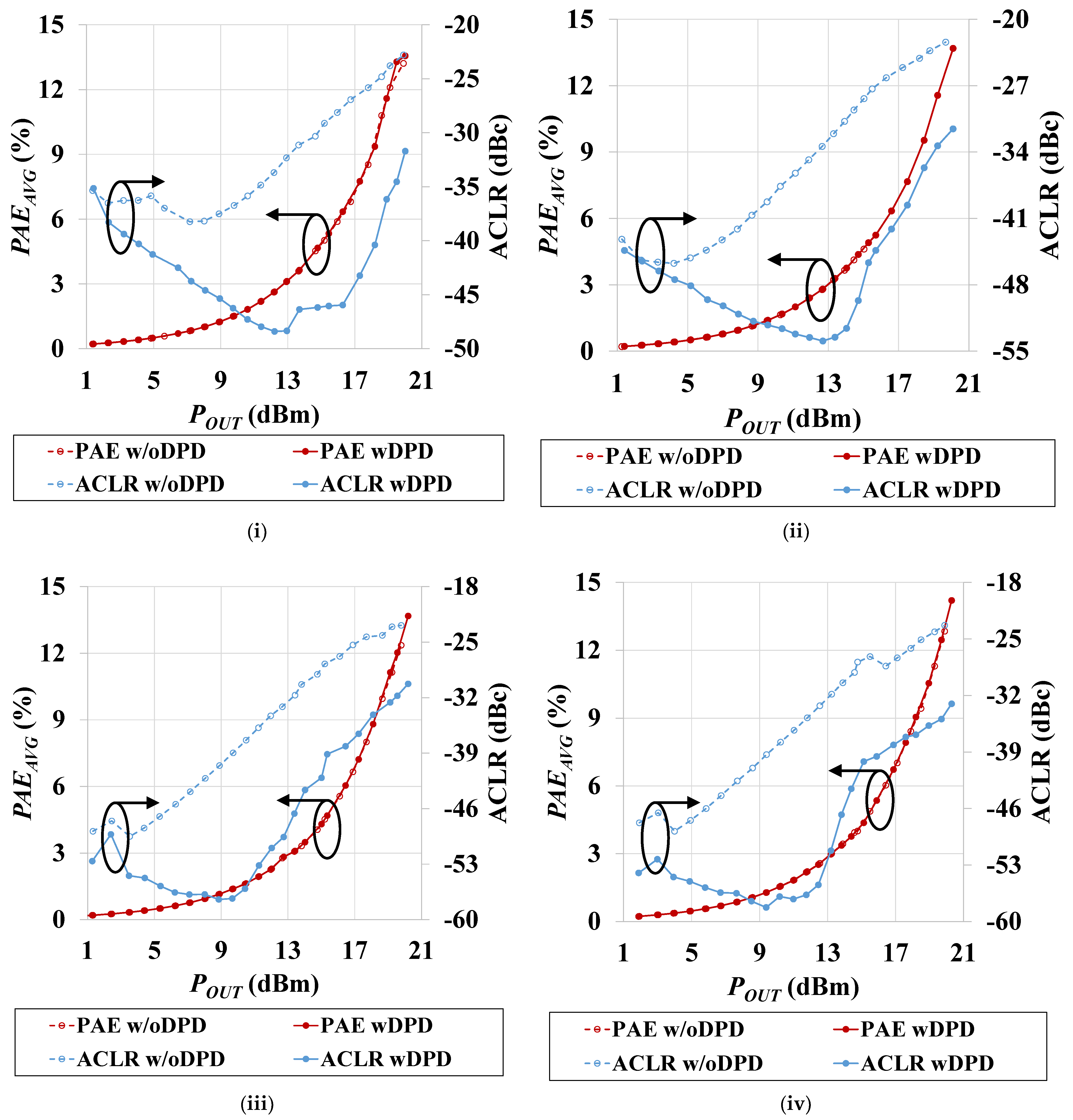
Figure 6 shows the comparison between
PAEAVG and ACLR vs. the
average POUT using a 5
20 MHz LTE 64-QAM signal with PAPR = 8 dB. The ACLR can improve very significantly using GMP DPD. At 24 GHz, ACLR with DPD has a consistent improvement of around 16 dB when the PA is operated with
average POUT = 14 dBm to 16 dBm. The ACLR with GMP DPD obtains the best improvement of around 22 dB when the PA is operated with
average POUT = 11 dBm at 39 GHz. At the common
average POUT of 15 dBm/20 dBm, this PA has an ACLR/PAE improvement of around 17 dB/0.3% using the 5
20 MHz LTE 64-QAM signal at 24 GHz. At 28 GHz and 37 GHz, there is a significant ACLR/PAE improvement of around 21 dB/1.3% and 21.5 dB/1.5%, operated with a common
average POUT of 13 dBm/20 dBm for both frequencies. The PAE has the highest improvement when the PA is operated with an
average POUT of 20 dBm at 24 GHz/28 GHz/37 GHz/39 GHz.
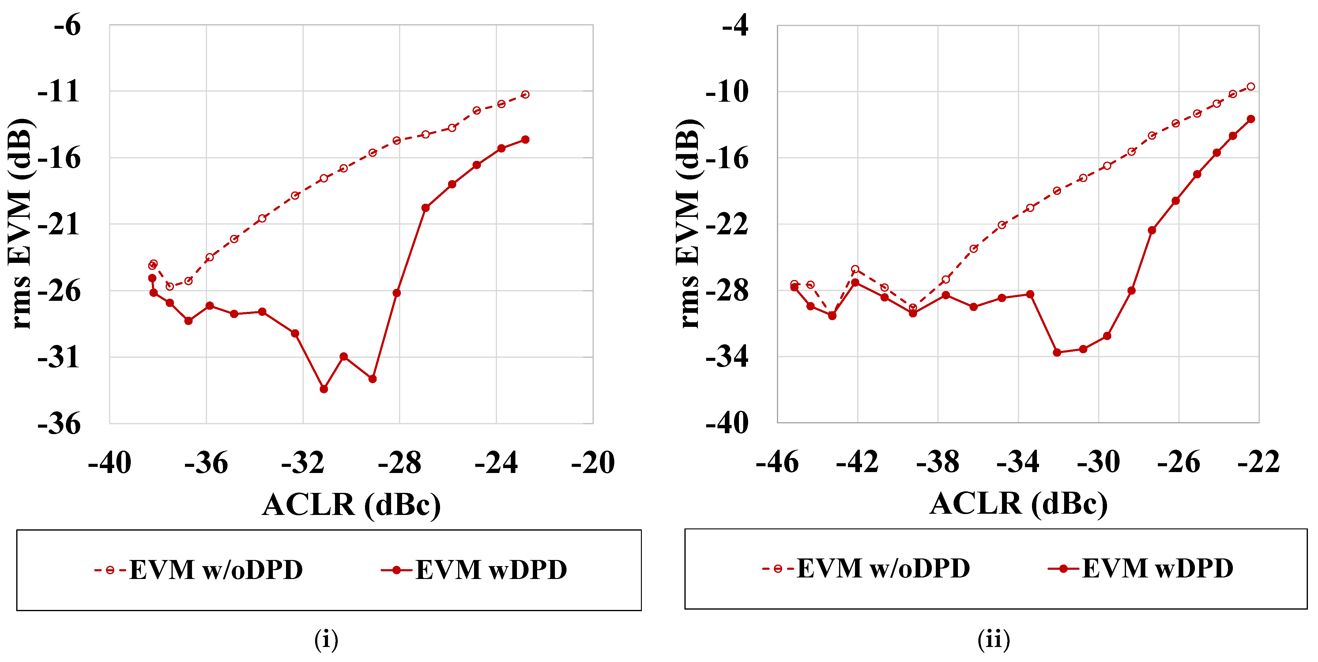
The EVM of the PA (i.e.,
) is determined from Equation (11). The intrinsic EVM (
is determined by having a thru connection between the two mm-Wave radio head 5582 devices as shown in
Figure 2.
is determined by just connecting the driver in between the mm-Wave radio head 5582 devices and measured across the similar powers of the PA.
is the EVM from the mm-Wave DPD experiment shown in
Figure 2. Substituting each in Equation (11) gives the
.
The two-stage GaN PA after GMP DPD has an EVM that is reduced from −15.64 dBc to −32.65 dBc (an improvement of around 17 dB), with an improved ACLR of around −29 dBc using the 5
20 MHz LTE 64-QAM input of PAPR = 8 dB at 24 GHz. With an ACLR of around—30 dBc, the PA after DPD has an EVM reduction of around 15.5 dB at 28 GHz. As shown in
Figure 7, the EVM of the PA has a major reduction when the ACLR is from around −32 dBc to −28 dBc for both 24 GHz and 28 GHz.
Figure 8 showcases the EVM reduction in the PA across signals of different bandwidths as modulated signals. The PA is tested using a 1
20 MHz, 2
20 MHz 4
20 MHz and 5
20 MHz LTE 64-QAM input of PAPR = 8 dB at 28 GHz. The PA after DPD has a very large EVM reduction of around 25 dB, with an ACLR of around −34 dBc using a 4
20 MHz 64-QAM 4G LTE input at 28 GHz. This highlights that the GMP DPD works well on both narrower-band (1
20 MHz) and wider-band (5
20 = 100 MHz) LTE 64-QAM signals. The EVM consistently has a reduction of greater than 10 dB using the 1
20 MHz LTE 64-QAM input of PAPR = 8 dB at 28 GHz. For the 2
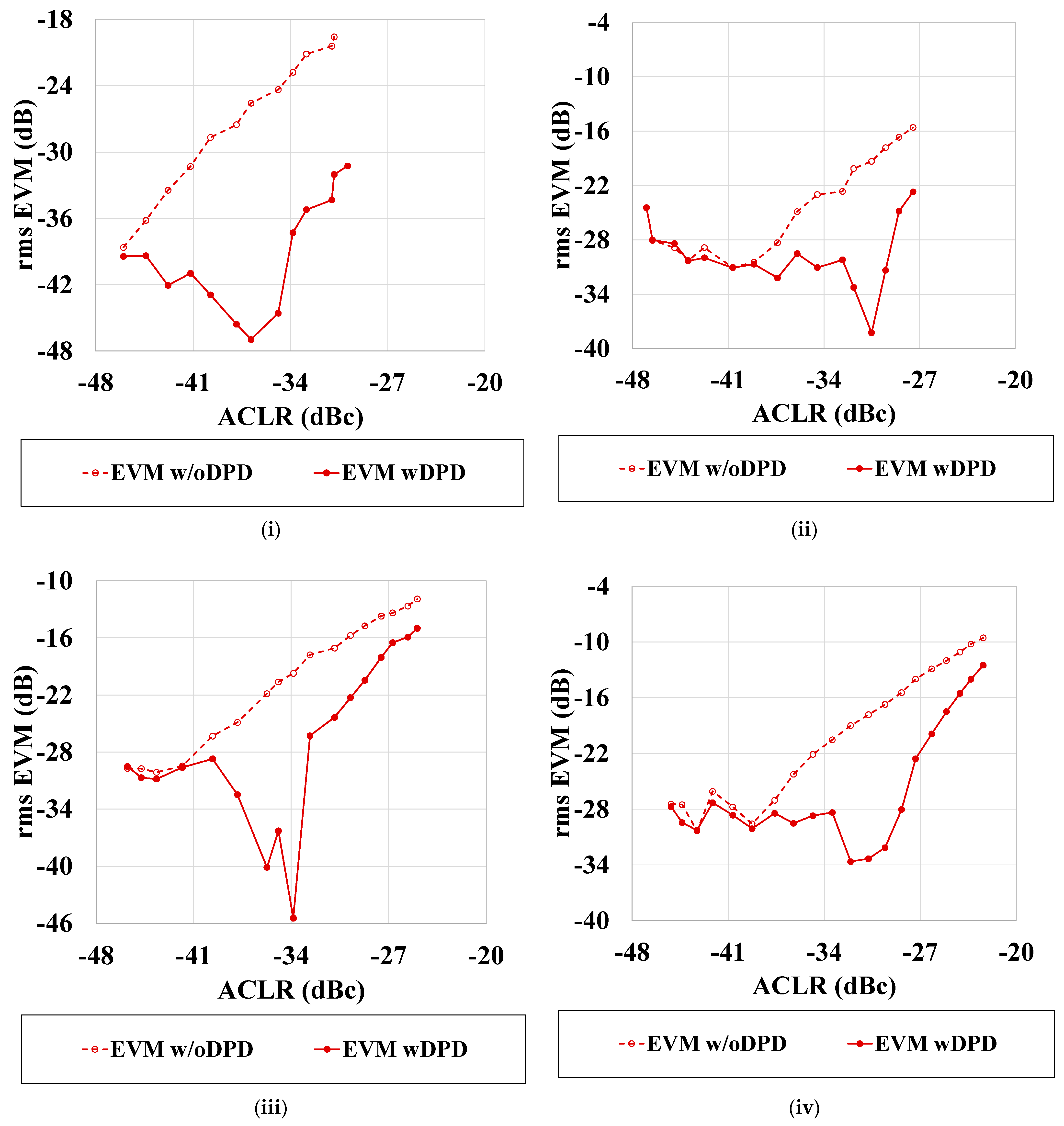
20 MHz LTE 64-QAM input at 28 GHz, the EVM of the PA after DPD reduces from −19 dBc to around −38 dBc, with an ACLR of ~−30 dBc. The rms (root-mean-square) EVM and ACLR of the PA shown in
Figure 8 are measured from a common range of
average POUT = 1 dBm to 20 dBm. With the common x-axis scale for the ACLR ranging from −48 dBc to −20 dBc, we could see that before DPD is applied, the measured rms EVM data are pretty much linearly proportional to the corresponding measured ACLR data, regardless of the signal BW. However, once GMP DPD is applied, the EVM is reduced considerably at the same level of the ACLR, and the EVM and ACLR are no longer linearly correlated for a large range of ACLR values. For example, at the common ACLR of −34 dBc, the measured EVM values before DPD for the 1
20 MHz/2
20 MHz/4
20 MHz/5
20 MHz signal BW are around −23 dBc/−23 dBc/−20 dBc/−21 dBc, while after the GMP DPD they become greatly reduced to around −37/−30/−46/−28 dBc. As bandwidth increases from 1
20 MHz to 5
20 MHz, the rms EVM plot moves to a higher ACLR (−20 dBc) region on the x-axes in general. The more precise BW effects on ACLR and rms EVM at higher
average output powers such as 15 dBm and 20 dBm can be seen in later figures which are to be discussed later.
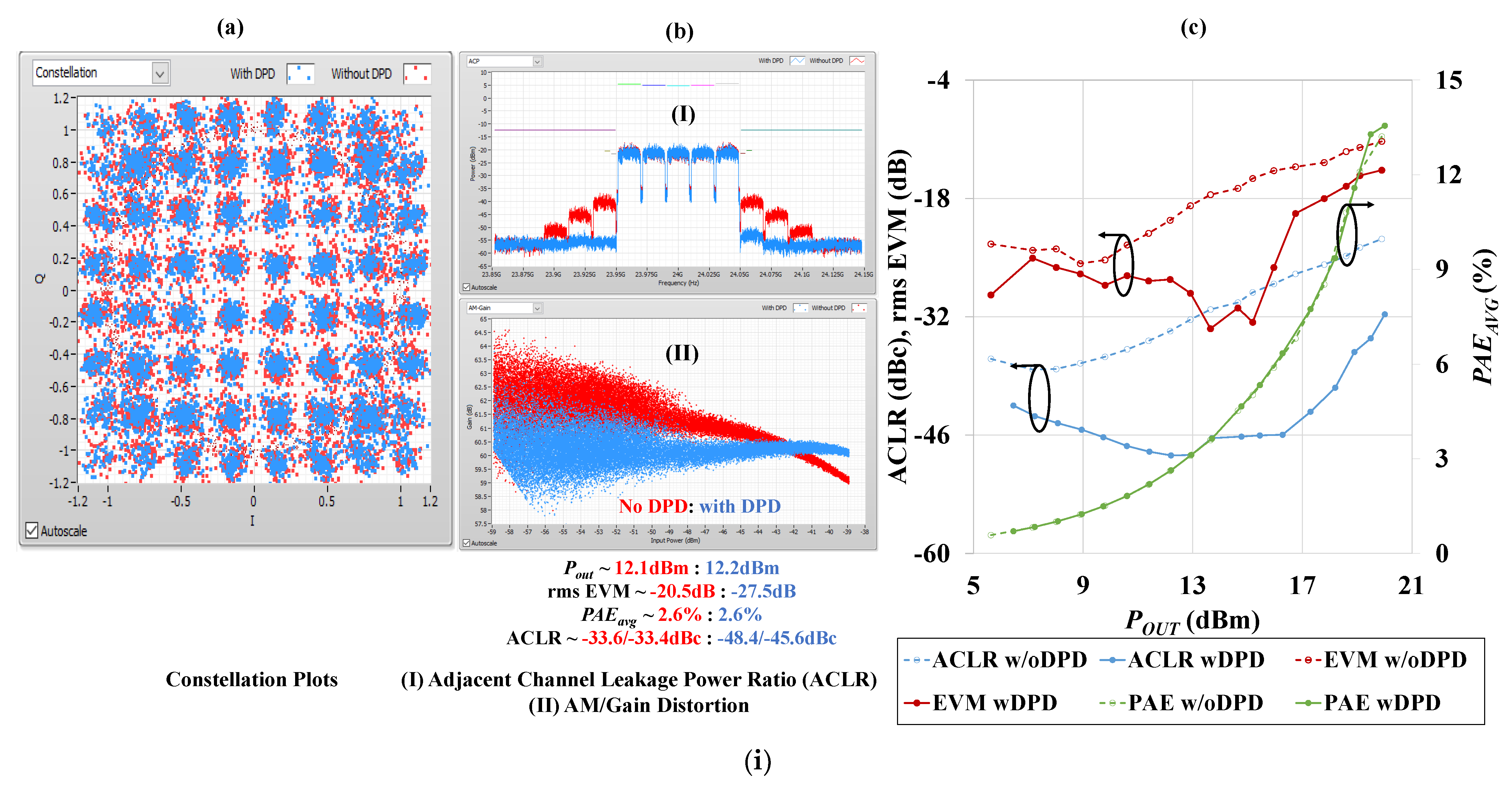
The measured constellation diagram and AM/gain distortion of the PA are shown in
Figure 9. The PA is tested using the 5
20 MHz LTE 64-QAM modulated signal input of PAPR = 8 dB at 24 GHz/28 GHz/37 GHz/39 GHz with/without the GMP DPD.
Figure 9(I) presents the measured rms EVM, ACLR and
PAEAVG vs. the PA’s
average POUT at relatively higher output power levels (i.e.,
average POUT = 6 dBm to 20 dBm) at a given mm-Wave frequency (four plots, (i)–(iv), at 24 GHz/28 GHz/37 GHz/39 GHz, respectively).
Figure 9(i–iv)(a,b) shows the PA transmit output spectrum, constellation diagram and AM/gain distortion curve when the PA is operated at
average POUT~12 dBm at a given frequency ((i)–(iv), 24–39 GHz, using the 5
20 MHz LTE 64-QAM signal input of PAPR = 8 dB). At 24 GHz, with an
average POUT~12 dBm and after applying the GMP DPD, the GaN PA has a rms EVM reduction from −20.5 dBc to −27.5 dBc, and an ACLR improvement of around 15 dB. The non-linear AM/fain distortion curves are plotted with an input power of −59 dBm to −38 dBm on the horizontal axis, which corresponds to an absolute
PIN of −18 dBm to 3 dBm due to the 41 dB attenuation used in the setup for 24 GHz. The PA output spectrum at 24 GHz shows that its ACLR +/− is −33.6 dBc/−33.4 dBc before the GMP DPD, and after the GMP DPD a significant reduction in the ACLR +/− of −48.4 dBc/−45.6 dBc is observed. We can also see from the constellation diagram before the DPD, that the symbols are more scattered and rotated (in red), but after the GMP DPD, these symbols are slightly better aligned and centered at
POUT~12 dBm (in blue). The relationship of ACLR, rms EVM and
PAEAVG is also plotted against the
average POUT at each frequency in
Figure 9, which shows that at a higher
average POUT, the PA’s linearity will inevitably degrade with a higher ACLR and rms EVM, but the PA will also have higher efficiency as it is more saturated (e.g.,
PAEAVG~11% to 14%) with a larger
average POUT (e.g., 18 dBm to 20 dBm). At these higher
average POUT levels of 18–20 dBm, the corresponding peak
POUT is close to the Watt level (i.e., 26–28 dBm), and the rms EVM values are around −18 dB to −12 dB and ACLR~−40 dBc to −32 dBc without DPD. After the GMP DPD is applied, the rms EVM and ACLR can be improved by ~10 dB and 3–4 dB, respectively, at these high
POUT levels where the PA is a bit more nonlinear. From the 4–6 dB power back-off levels at 24 GHz where the
average POUT is 14 dBm to 16 dBm, the PA can have an excellent ACLR of ~−46 dBc after the GMP DPD, where the rms EVM and ACLR can both be improved by ~15 dB or more, with a
PAEAVG of 4% to 6%. Similarly,
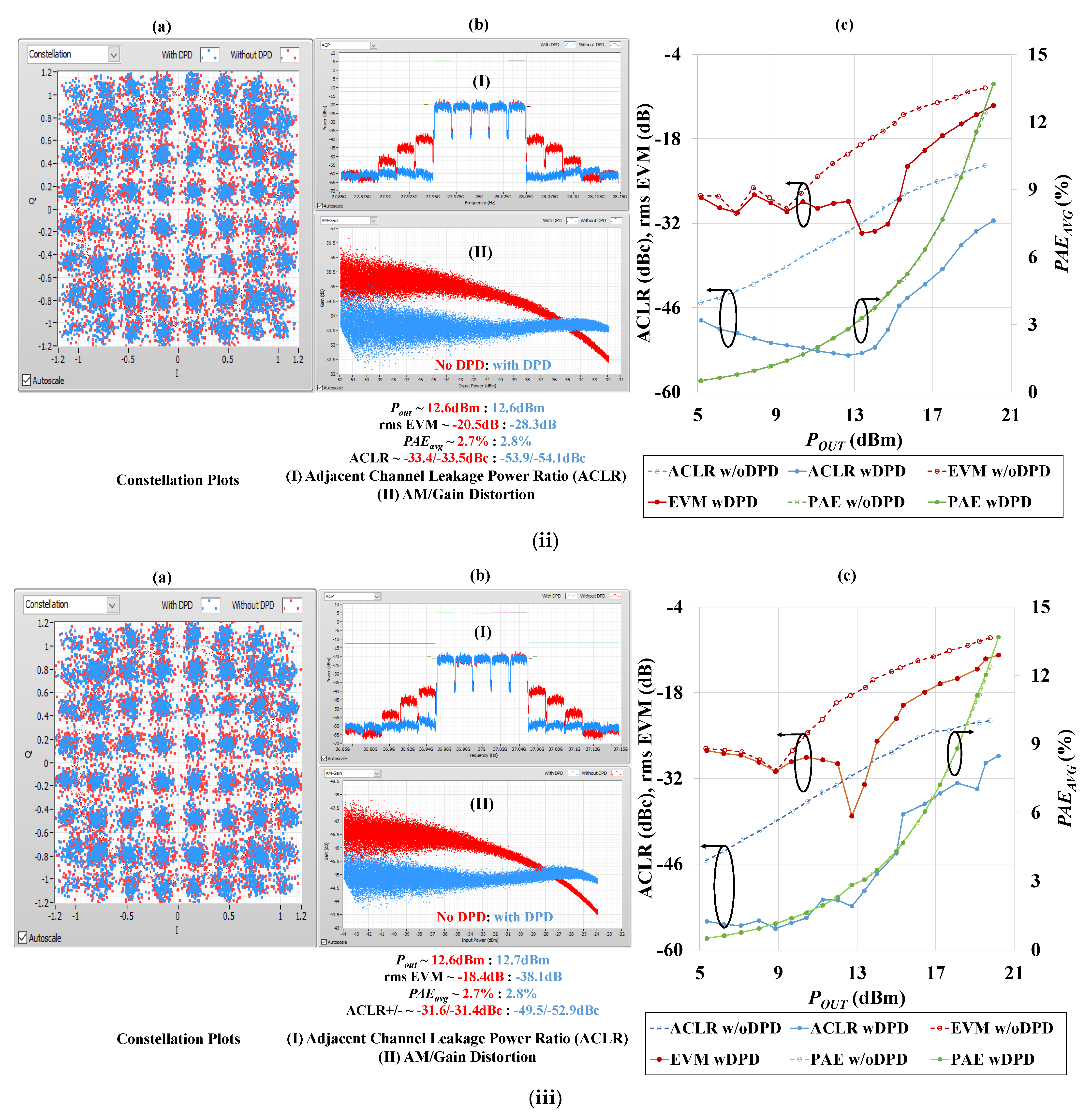
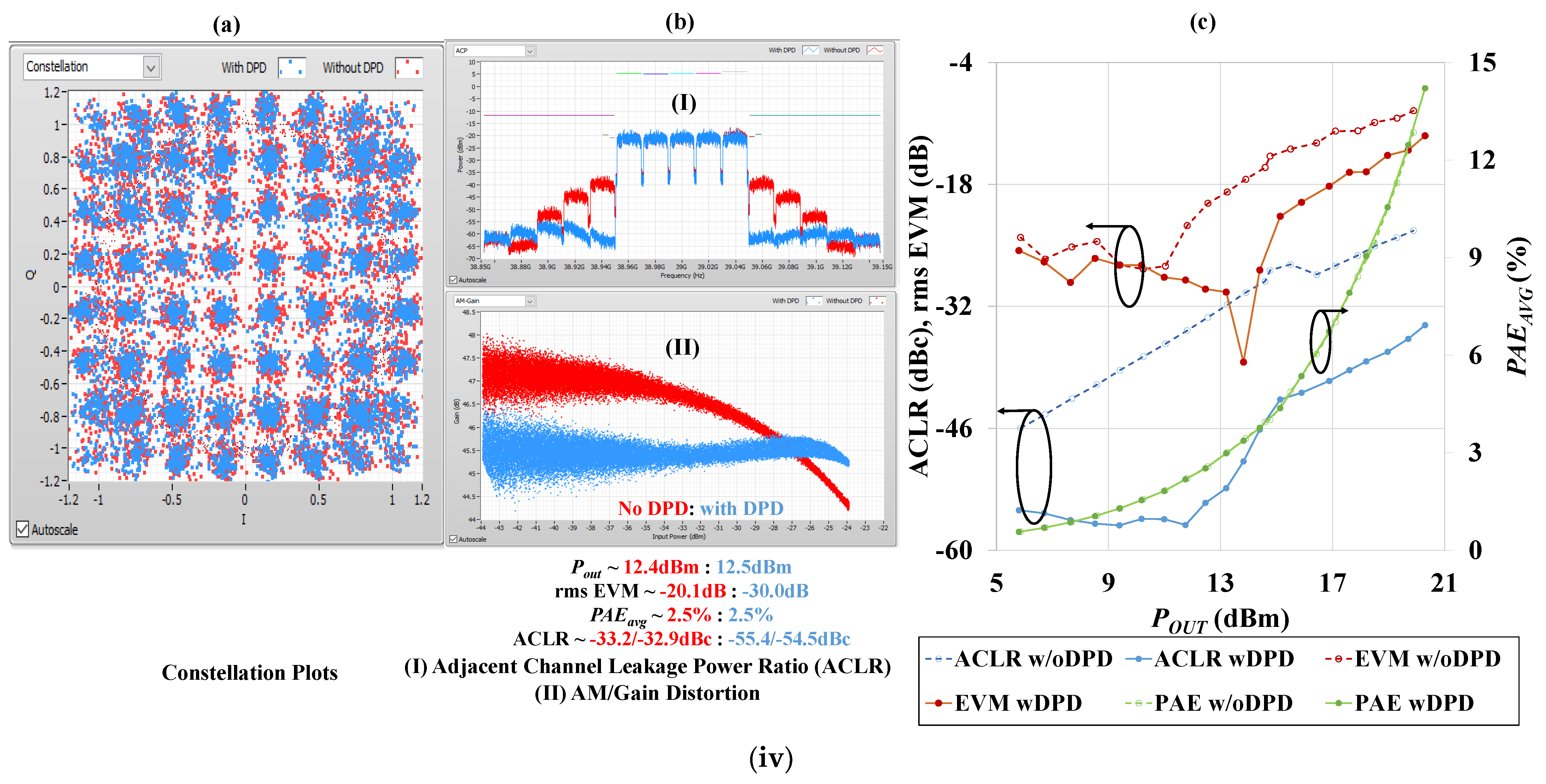
Figure 9 shows that at 28 GHz/37 GHz/39 GHz, when the
average POUT is from 13 dBm to 15 dBm, the PA has an outstanding ACLR from −50 dBc to −46 dBc, −52 dBc to −46 dBc, and −52 dBc to −46 dBc, respectively.
As also seen from
Figure 9ii(b)–iv(b), the PA transmit output spectra before/after the GMP DPD show that the PA has a rms EVM reduction of from −20.5 dB to −28.3 dB/−18.4 dB to −38.1 dB/−20.1 dB to −30.0 dB, an ACLR improvement of around 21 dB/21 dB/22 dB, and a PAE improvement of around 0.1%/0.1%/0.0% with GMP DPD at 28 GHz/37 GHz/39 GHz, respectively. We also see that the PA transmit output spectrum after GMP DPD has an ACLR+/− of −53.9 dBc/−54.1 dBc and −55.4 dBc/−54.5 dBc at 28 GHz and 39 GHz, respectively. These good linearity data suggest that the PA memory effects are considerably reduced after using GMP DPD. The AM/fain non-linear distortion curve highlighted in red is shown in
Figure 9 as well. For 28 GHz/37 GHz/39 GHz, the PAs are linear as shown in blue highlights scaling from an input power of −40 dBm to −32 dBm/−32 dBm to −24 dBm/−32 dBm to −26 dBm at their respective frequencies. In
Figure 9i(b)–iv(b), the non-linearities of the PA transmit output spectra across the adjacent channels (in red) at a given center frequency (i.e., 24 GHz/28 GHz/37 GHz/39 GHz) are further worsened due to CA of the input modulated signal with 5
20 MHz, as similarly reported in Refs. [
21,
22]. This ACLR non-linearity increases as the operating frequency rises and is considerably reduced using GMP DPD (in blue). For example, looking at the adjacent channels of
Figure 9 at 24 GHz (from 24.05 GHz to 24.15 GHz) with the BW of 5
20 MHz, we see that the ACLR jumps (in red) become a bit further reduced after applying GMP DPD (in blue), and they increase as the frequency increases to 28 GHz/37 GHz/39 GHz.
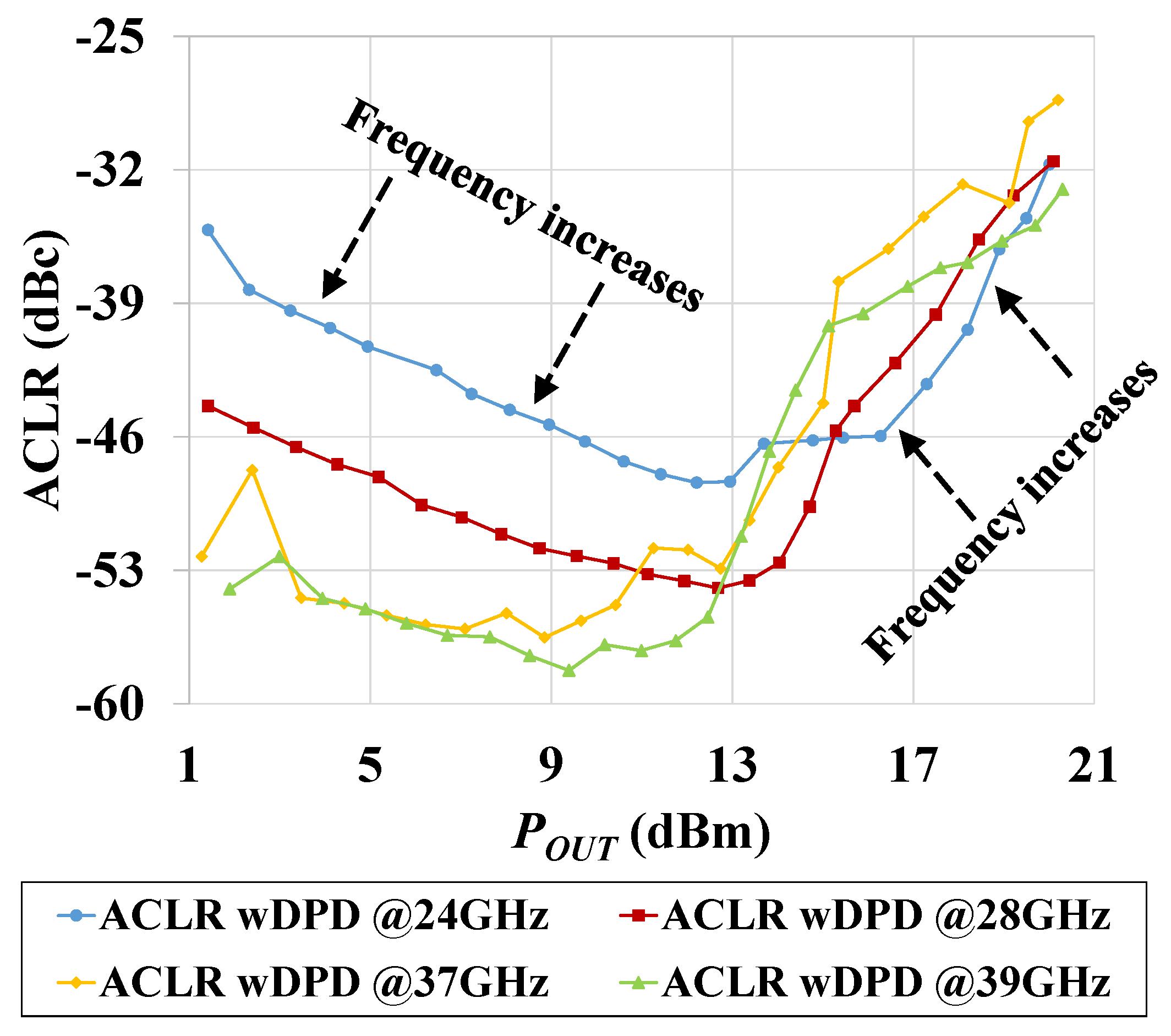
Figure 10 demonstrates the ACLR improvement across various frequencies and
average POUT values using a 5
20 MHz LTE 64-QAM input signal of PAPR = 8 dB. The PA after GMP DPD has an excellent ACLR improvement for the lower
average POUT levels (say, an
average POUT of ≤ 13 dBm) at all frequencies, while the best ACLR happens at the highest frequency of 39 GHz and the ACLR worsens as frequencies become lower, reaching the worst ACLR at 24 GHz. The measured ACLR reaches around −59 dBc at 39 GHz at the
average POUT of 9 dBm, which is the best ACLR level for all cases presented in this work. However, as the PA is operated at a higher
average POUT from 15 dBm to 21 dBm, the lowest ACLR now happens at the
lowest frequency of 24 GHz, and worsens as the frequencies become higher, reaching the worst ACLR at the highest testing frequency of 39 GHz. Therefore, this trend of reaching the best ACLR over the frequencies depends on the
average POUT level, and interestingly it changes around the
average POUT level of around 13 dBm, suggesting that it would be very challenging to use the same GMP DPD algorithm to produce a broadband PA [
23,
24] linearity improvement consistently with a large
average POUT level and frequency range. The linearity improvement is mostly independent of the operation frequency of the broadband mm-Wave PAs tested in this work, which is encouraging as this demonstrates the effectiveness of the GMP DPD model used. The bandwidth effects of the LTE 64-QAM input signal on the PA’s ACLR are shown in
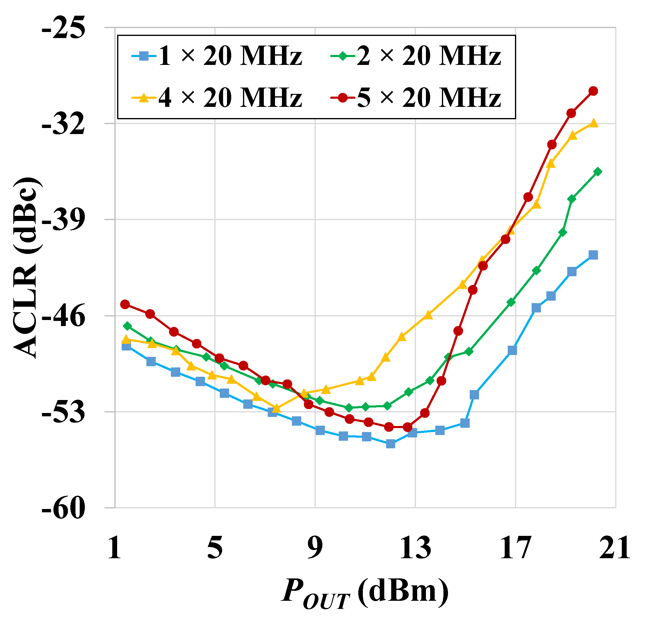
Figure 11 at the single frequency of 28 GHz. We can see that the PA’s ACLR after GMP DPD using a 1
20 MHz 64-QAM 4G LTE input of PAPR = 8 dB is better than those from the 2
20 MHz/4
20 MHz/5
20 MHz LTE 64-QAM input. It appears that the wider the modulated signal BW, the worse the ACLR becomes. However, evidently when the PA is operated with an
average POUT of 13 dBm, the ACLR after GMP DPD the using 1
20 MHz and 5
20 MHz LTE 64-QAM input of PAPR = 8 dB modulated signals at 28 GHz are equally around -54 dBc. As discussed earlier, we can see that the ACLR decreases from −30 dBc to −43 dBc as the signal bandwidth decreases from 5
20 MHz to 1
20 MHz at an
average POUT of 20 dBm, which describes the BW effect on the ACLR. This BW effect similarly occurs with the lower input power as well. The trend changes for the
POUT from 9 dBm to 15 dBm as the ACLR of 5
20 MHz is greater than the ACLR of 2
20 MHz and 4
20 MHz at 28 GHz are due to the GMP DPD.
As the PA is operated at an average POUT greater than 17 dBm, the ACLR after GMP DPD becomes worse with a larger signal bandwidth. The ACLR values after GMP DPD are around −42 dBc/−36 dBc/−32 dBc/−30 dBc for the 1 20 MHz/2 20 MHz/4 20 MHz/5 20 MHz LTE 64-QAM modulated input signal operated with an average POUT of 20 dBm.
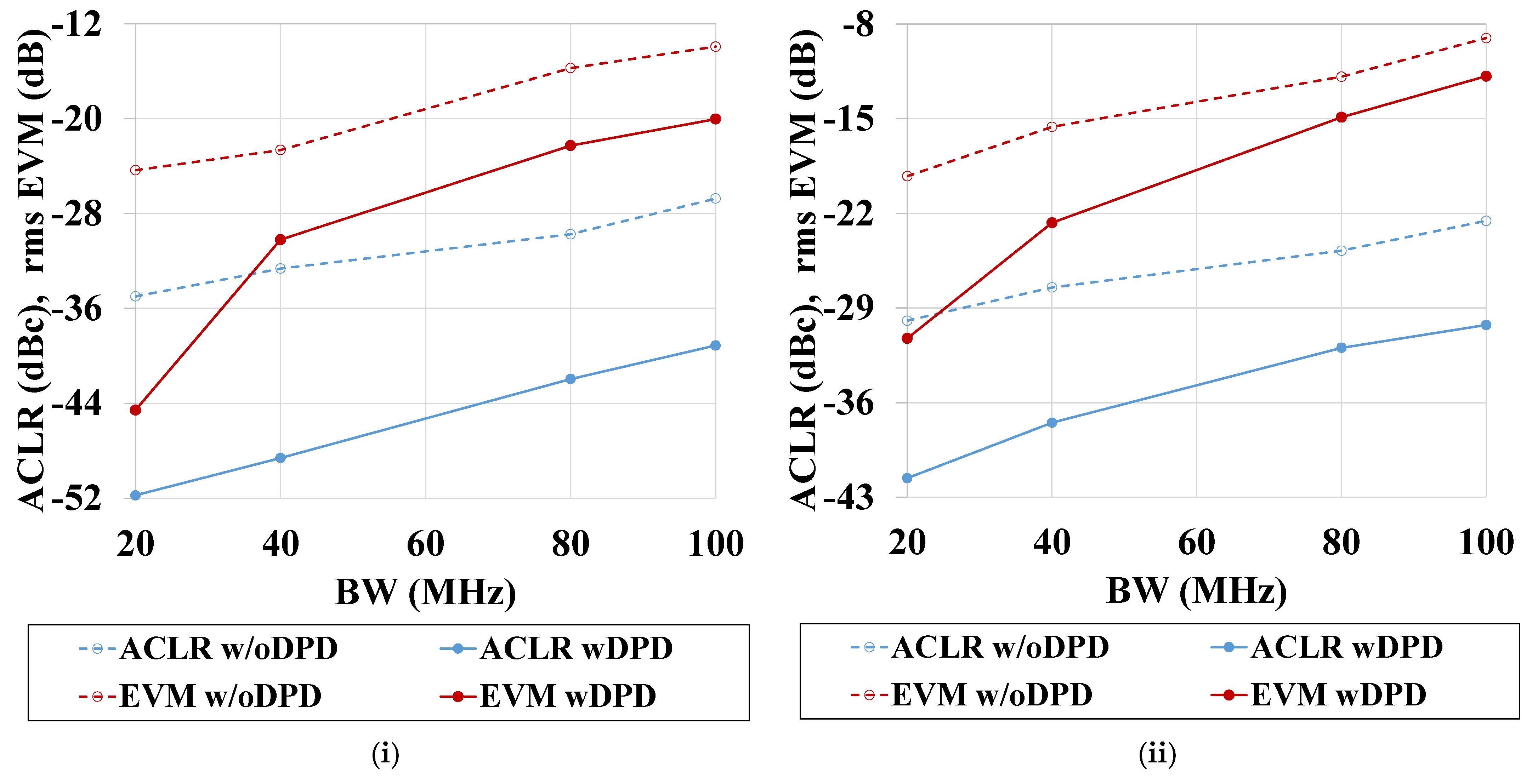
Figure 12 shows the modulated signal bandwidth effects on the rms EVM and ACLR across 1
20 MHz/2
20 MHz/4
20 MHz/5
20 MHz at a higher
average POUT (of ≥15 dBm and 20 dBm). At an
average POUT, MAX of 15 dBm, the rms EVM/ACLR after GMP DPD improves from −24.3 dB/−34.9 dBc to −44.5 dB/-51.7 dBc; from −22.6 dB/−32.6 dBc to −30.2 dB/−48.6 dBc; from −15.7 dB/−29.7 dBc to −22.2 dB/−41.9 dBc; and from −13.9 dB/−26.7 dBc to −20.0 dB/−39.1 dBc using the corresponding 1
20 MHz, 2
20 MHz, 4
20 MHz, and 5
20 MHz LTE 64-QAM input signals. When the
average POUT, MAX = 20 dBm, the rms EVM/ACLR after GMP DPD improves from −19.2 dB/−29.9 dBc to −31.2 dB/−41.5 dBc; −15.6 dB/−27.4 dBc to −22.7 dB/−37.4 dBc; −11.8 dB/−24.7 dBc to −14.8 dB/−31.9 dBc, and −9.0 dB/−22.5 dBc to −11.8 dB/−30.2 dBc using the 1
20 MHz, 2
20 MHz, 4
20 MHz and 5
20 MHz LTE 64-QAM input signals, respectively. The difference in the ACLR after GMP DPD decreases as the bandwidth is increased for both cases of
average POUT of 15 dBm and 20 dBm. This trend is also similar to the ACLR for the rms EVM to reduce after DPD, and it also worsens as the signal bandwidth increases. Wideband-modulated 5G signals are achieved using CA. The distortion worsens as the signal BW increases, with a higher AM/AM and with the rms phase error of AM/PM rising as the signal BW increases, as well as worsened ACLR and EVM values. However, considerable linearity improvements are seen after GMP DPD, which are especially relevant and critical to extending mm-Wave GaN PAs for mm-Wave applications that require larger
POUT, Linear values such as 5G small cells.


 and
and 


