Article

Performance Evaluation of Solar-PV-Based Non-Isolated Switched-Inductor and Switched-Capacitor High-Step-Up Cuk Converter

by
Neeraj Priyadarshi
1,
Mahajan Sagar Bhaskar
2,
Farooque Azam
3,
Mayank Singh
4,
Dheeraj Kumar Dhaked
4,
Ibrahim B. M. Taha
5 and
Mohamed G. Hussien
6,*
1
Department of Electrical Engineering, JIS College of Engineering, Kolkata 741235, India
2
Renewable Energy Lab, College of Engineering, Prince Sultan University, Riyadh 11586, Saudi Arabia
3
School of Computer Science and Engineering, REVA University, Bangalore 560064, India
4
Department of Electrical Engineering, Rajasthan Technical University, Kota 324010, India
5
Electrical Engineering Department, College of Engineering, Taif University, P.O. Box 11099, Taif 21944, Saudi Arabia
6
Electrical Power and Machines Engineering Department, Faculty of Engineering, Tanta University, Tanta 31527, Egypt
*
Author to whom correspondence should be addressed.
Electronics 2022, 11(9), 1381; https://doi.org/10.3390/electronics11091381
Submission received: 23 February 2022 / Revised: 18 April 2022 / Accepted: 22 April 2022 / Published: 26 April 2022
(This article belongs to the Special Issue Advancement in Power Electronics and Control)

Abstract

:
Solar photovoltaic (PV) is the most promising renewable energy source available on Earth. Three topologies based on a switched-inductor capacitor and non-isolated high-step-up Cuk converter have been proposed for solar PV. These topologies of the Cuk converter have higher boosting ability than conventional Cuk and boost converters and can reduce the voltage stress of the main switch. A small voltage rating and on-state resistance can give higher efficiency of the converter. The voltage boosting ability of all three topologies was compared to each other and with a conventional Cuk converter. The boosting capability of the third converter was 11 times at 0.75 duty cycle with a solar PV source. These converters do not use a coupled inductor and transformer, which leads to less volume, reducing coupling/core saturation loss, and thus the cost of the converter. A solar PV system of 12 volts was used for boosting with these converters for analysis of the feasibility of use with renewables. The three topologies of the switched-inductor and switched-capacitor (SLSC) Cuk converter were designed and simulated in MATLAB/Simulink to evaluate their effectiveness.

1. Introduction

World energy demand is growing linearly while fossil fuel supplies, such as petroleum, coal, and natural gases may be depleted in the near future. The major issues with fossil-fuel-based energy generation are greenhouse gas emissions and carbon footprint. The growing energy demand cannot be met solely through sources such as thermal, hydro, nuclear, etc. As a result, it is essential to use alternative energy or renewable energy sources which are abundant and freely available to overcome the global energy crisis and meet future energy demands. Solar energy is of the utmost importance among renewable energy sources because it is pollution-free and inexhaustible [1]. Its use is becoming increasingly common these days because non-renewable energy can harm and affect the environment and nature. The key advantages of photovoltaic (PV) applications are that they are clean, emission free, and have a high level of reliability [2]. PV cells are used to extract a usable electrical form of energy from solar energy. Renewable energy sources, such as solar, give low voltage output that needs to be boosted to higher functional levels [3,4]. The primary consideration in renewable applications is how to achieve high voltage gain while maintaining more efficiency during voltage boosting. By 2040, PV will be the most crucial source of power generation among all renewable energy candidates [5].
DC to DC conversion is now employed in numerous sectors and applications, including renewable sources, EV charging stations, uninterrupted power supply, electric trains, and others [6]. Low DC output voltages are standard in PV and fuel cells, requiring high voltage gain DC-DC converters to connect them to the grid [7,8,9,10]. The converter must have a steady input current to obtain extreme power from the solar panels. More voltage gain from an uninterrupted input supply current determines the suitability of converters for renewable energy applications [11,12]. A novel continuous step/down and step switched-capacitor (SC)-based DC-DC converter has been suggested to have many advantages, such as lower voltage stress for capacitors and higher voltage gain than formerly proposed DC-DC converters [13]. In another paper, a new high voltage amplification DC-DC converter with a coupled inductor and voltage multiplier (VM) cell is described. Converter behavior is relied on for charging capacitors using a single MOSFET switch and adding sources in series from the source to the load [14]. A novel non-solidified DC-DC Cuk and boost converter assembly with high voltage amplification is proposed. The presented topology consists of a boost and a Cuk converter with a low power voltage ripple and high voltage gain in comparison to the conventional boost and Cuk converter [15]. In [16], an effective method based on the Harris Hawks optimization algorithm (HHO) to select the optimal capacity, number, and location of solar-based DGs to reduce active power loss and voltage deviation is used. The authors of [17] describe the improvement in an effective non-isolated switched-capacitor coupled-inductor boost-converter structure. Switched capacitors decrease the voltage stress of power semiconductor switches, reduce device conduction losses, and enable the use of low on-resistance switches. In addition, passive clamp circuits can be used to achieve zero current to turn diodes and solid-state power switches on and off naturally [17]. A high static gain DC-DC converter with a single switch for efficient photovoltaic (PV)-based grid applications is proposed in [18]. This proposed topology is derived from SEPIC (single-ended primary inductor converter) by presenting a voltage doubler circuit to reduce voltage stress across semiconductor devices and provide high voltage gain [18].
This research study considers the requirement by renewable energy applications for high voltage gain with uninterrupted input supply current using a DC-DC converter. A solar PV system is used to generate three different topologies derived from a Cuk converter. The solar PV renewable source can reduce the effect of environmental deteriorating agents produced by conventional power generating stations. A conventional Cuk converter is modified to create three different topologies based on a switched-inductor and a switched-capacitor (SLSC). The improvement implemented involves putting an SC unit in the place of the capacitor, and placing an SL unit in the position of the inductors. The proposed converter produces less noise, has a high transient response, and has minimal electromagnetic interference. Climate issues lead to the degradation of photovoltaic panels; temperature is the most degrading factor for solar panels as they are exposed to sunlight [19,20,21]. This issue must be considered in countries such as India, Egypt, and Saudi Arabia; however, manufacturers’ statements are often given for lower temperatures and different conditions than the real-world conditions experienced. This paper does not consider the durability of panels.
The voltage boosting provided by these converters is negative to positive. The objectives of the study are as follows:
  • To introduce the basics of the Cuk converter and different derived topologies based on switched-inductor and switched-capacitor (SLSC) and a high-gain step-up Cuk converter.
  • To study a PV system with a DC-DC converter.
  • To implement the Simulink model of the three converters considered with solar PV on the MATLAB platform.
  • To study the behavior of the converter and analyze its characteristics.
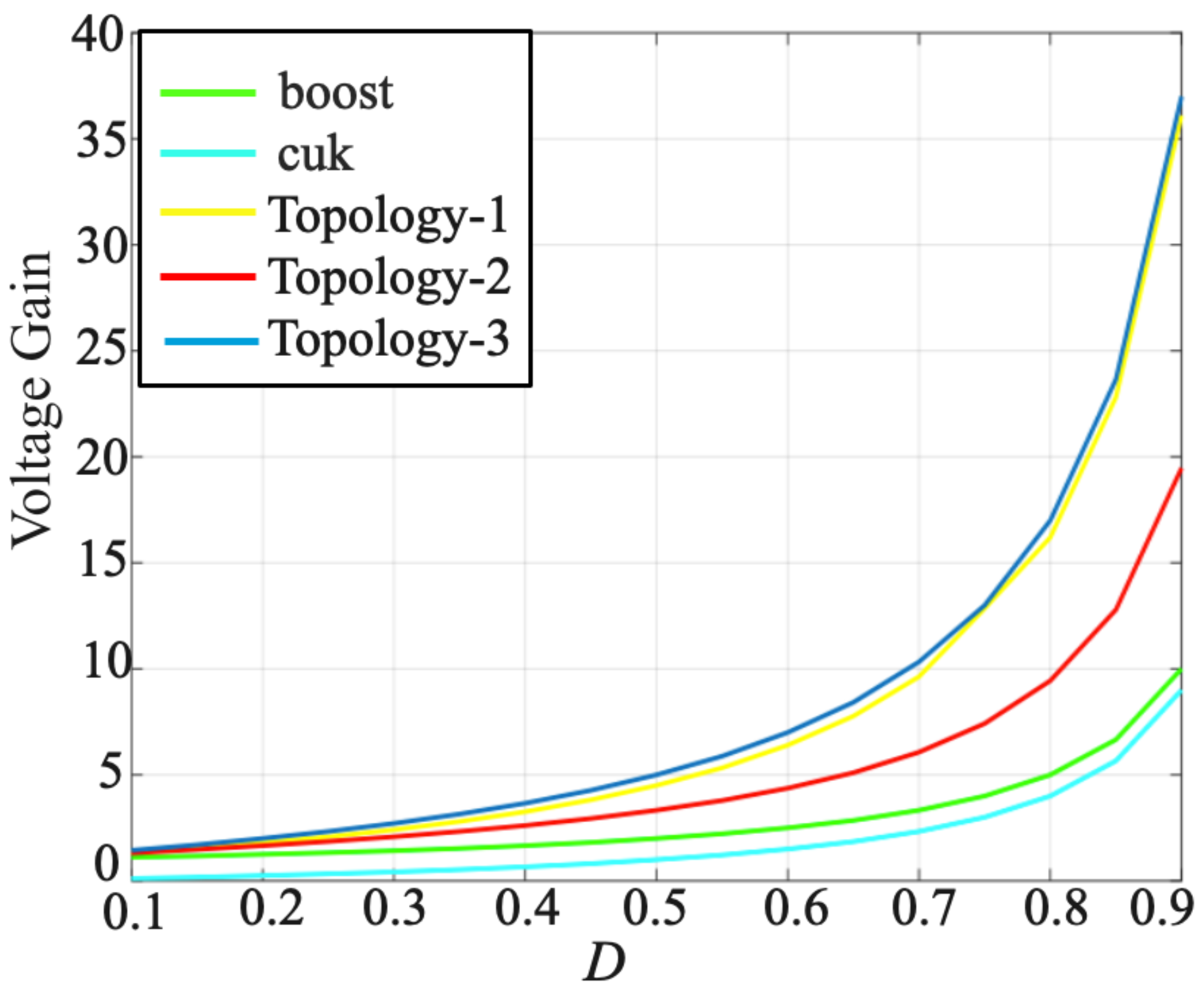
  • To compare the boosting ability of a conventional boost converter with the discussed topologies.

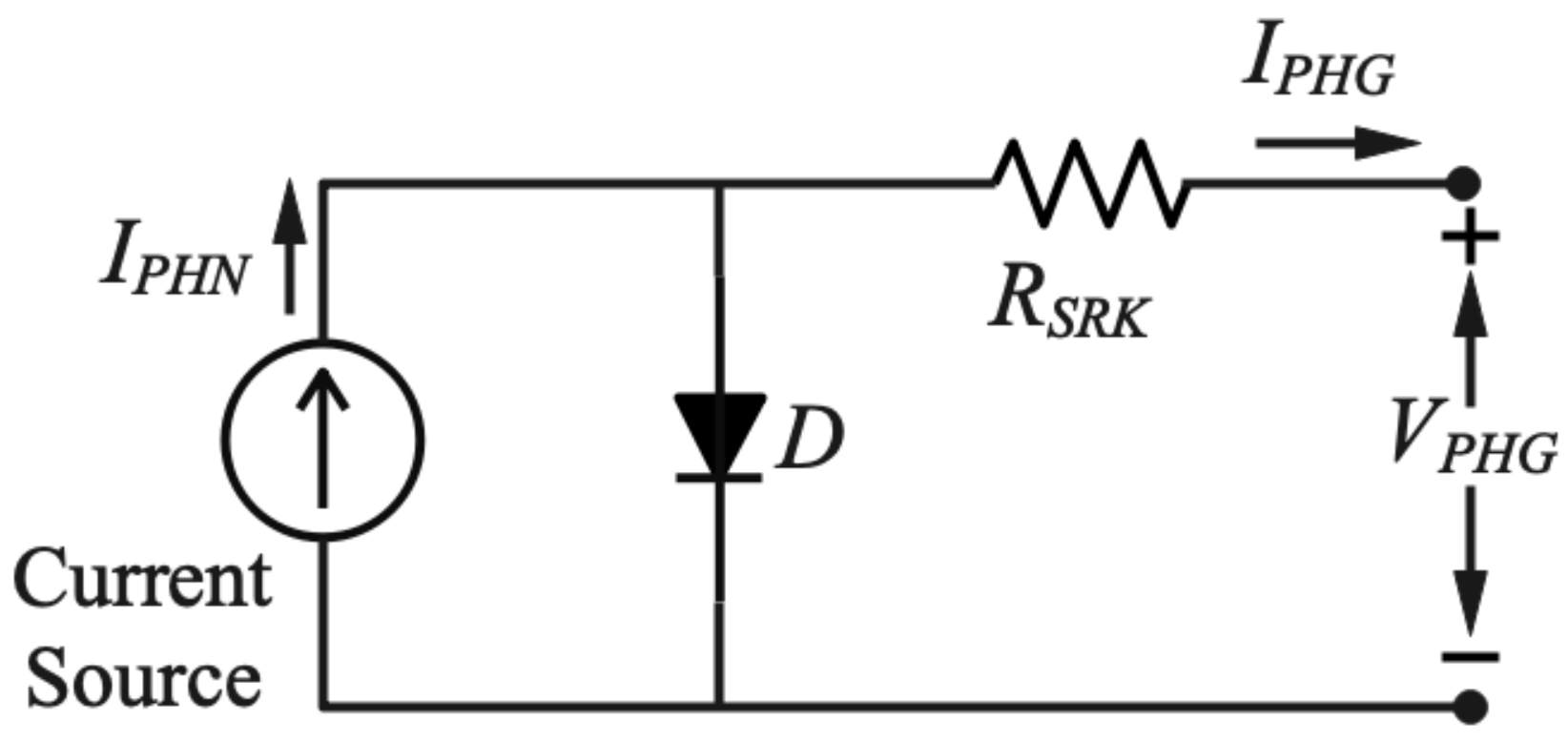
2. Photovoltaic Generator Mathematical Modeling

The PV array parameters depend on several environmental factors [22,23]. However, designers have only used parameters for standard test conditions (STC). Accurate PV modeling is essential to implement maximum power point tracking (MPPT) algorithms, and other controlling methods [24,25]. Hence, this research employed a modified uni-diode modeling (MUDM)-based PV system, which provides more straightforward implementation and reliable operation for power generation under varying atmospheric conditions. Compared to the ideal single diode model (ISDM) and the single diode model (SDM), modified uni-diode modeling (MUDM) enables more straightforward implementation. It also provides a more accurate response and easier modeling as ISDM and SDM do not provide precise I–V nature under the maximum power point (MPP) region and require more parameters for estimation, respectively [26].
The I–V curve of a PV module having N S R K cells connected in series (Figure 1) can be derived mathematically as:
I P H G = I P H N I S A T e Q E V P H G + I P H G R S R K N S R K N S R K K B T B A S 1 V P H G + I P H G R S R K N S R K N S R K R P a r a l l e l
where, I P H G is PV the output current, I P H N is the photon current, I S A T is the saturation current R S R K , R P a r a l l e l are the series and parallel resistor, A S is the diode ideality factor, Q E is the electronic charge, K B is the Boltzmann constant, T B is the module temperature, and N S R K is PV cells connected in series.
Mathematically, the I–V relation of the single diode model of a PV system can be expressed by putting R S R K = 0 in Equation (1) as:
I P H G = I P H N I S A T e Q E V P H G + I P H G R S R K N S R K N S R K K B T B A S 1
I P H G , I S A T and I S A T can be evaluated using the below relations as:
I P H G = G I R ( I s h o r t + α C T Δ T B )
where, G I R is the solar insolation (W/m 2 ), I s h o r t is the short-circuited current at standard test condition, Δ T B is the temperature difference, and α C T is the coefficient of current temperature. Moreover, I s h o r t can be evaluated mathematically as:
V o p e n ( G I R , T B ) V o p e n ( G I R , T S T C ) = | β V T | Δ T B
where, V o p e n ( G I R , T B ) is the open-circuited voltage at temperature T B , V o p e n ( G I R , T S T C ) is the open-circuited voltage at T S T C , and | β V T | is the absolute value of the coefficient of the voltage temperature.
Putting I P H G = 0, V o p e n can be evaluated as:
V o p e n = N S R K K B T B A S Q E ln I P H G I S A T + 1
Hence, V o p e n ( G I R , T B ) and V o p e n ( G I R , T S T C ) shall be evaluated through Equation (5) and refreshing Equation (4) as:
N S R K K B A S Q E T B ln G I R I s h o r t + α C T Δ T B I s h o r t + 1 T S T C G I R I s h o r t I R S + 1 = β V T Δ T B
Moreover, I S A T can be evaluated by the following expressions as:
I S A T = e β V T Δ T B Q E N S R K K B T B A S G I R I s h o r t + α C T Δ T B G I R I s h o r t I R S + 1 T S T C T B e β V T Δ T B N S R K K B T B A S
where, I R S is the reverse saturation current at standard test condition.
I R S = I s h o r t e Q E V o p e n N S R K K B T S T C A S 1
Moreover, V m a x and I m a x under MPP can be correlated mathematically as:
I m a x = I s h o r t I R S e Q E V m a x N S R K K B T S T C A S 1
From Equations (8) and (9),
I m a x I s h o r t = e Q E V m a x N S R K K B T S T C A S I s h o r t I m a x I s h o r t e Q E V o p e n N S R K K B T S T C A S

3. Hybrid Fuzzy-Logic Sliding Mode Control Based MPPT

In this study, a hybrid fuzzy-logic sliding-mode control (HFLC-SMC)-based MPPT controller was employed in which the fuzzy logic control provides production of V R e f which assimilates with MPP. The entire block diagram is presented in Figure 2. SMC delivers tracking of V R e f produced by the FLC controller using proper adjustment of the duty ratio of the Cuk-SEPIC converter, which results in the generation of zero difference of V P V and V R e f . The fuzzy-logic controller provides accurate responses and does not require any mathematical analysis.
The membership function of error and change in error can be expressed mathematically as:
E e r r o r P = P P V G P k P P V G P k 1 V P V G P k V P V G P k 1
d E e r r o r P = E e r r o r P k E e r r o r P k 1
where, P P V G ( P k ) is the instantaneous PV power, V P V G ( P k ) is the output PV voltage, P k is the sampling period.
The fuzzy logic output V R e f can be processed using a sliding mode controller and imposed to the Cuk-SEPIC converter. Considering the reference voltage of the PV module V R e f and the output PV voltage V P V G as controlling parameters of SMC, the sliding area can be expressed mathematically as:
S A r e a = K + d d t E e r r o r R 1
where, R is the relative degree.
E e r r o r = E r r o r = V P V G V R e f
Y ˙ = V ˙ P V G = I P V G C P V G I L K C P V G
Y ¨ K = 1 C P V G I ´ P V G 1 C P V G 1 L K V P V G 1 L K 1 d K V o u t
Put R = 2 in Equation (13),
S A r e a = K + d d t E e r r o r = K E e r r o r + = E ˙ e r r o r
S ˙ A r e a = Y ˙ K Y R e f = I P V G C P V G I L K C P V G
Assuming Y ¨ K = 0,
E ¨ e r r o r = Y ¨ K and S ˙ A r e a = K V P V G ˙ + 1 C P V G I ´ P V G 1 L K V P V G 1 L K 1 d K V o u t
where, K is constant considering the Lyapunov stability function
S ˙ A r e a = λ S i g n S A r e a
where, λ is constant. Using Equations (19) and (20),
λ S i g n S A r e a = K V P V G ˙ + 1 C P V G I ´ P V G 1 L K V P V G 1 L K 1 d K V o u t
And d K , the duty ratio, can be evaluated as:
d K = λ S i g n S A r e a + K V P V G ˙ + 1 C P V G I ´ P V G 1 L K 1 d K L K C P V G V o u t

4. Topologies of the CUK Converter
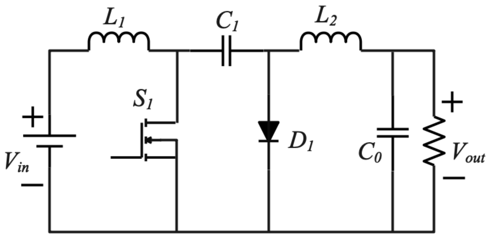
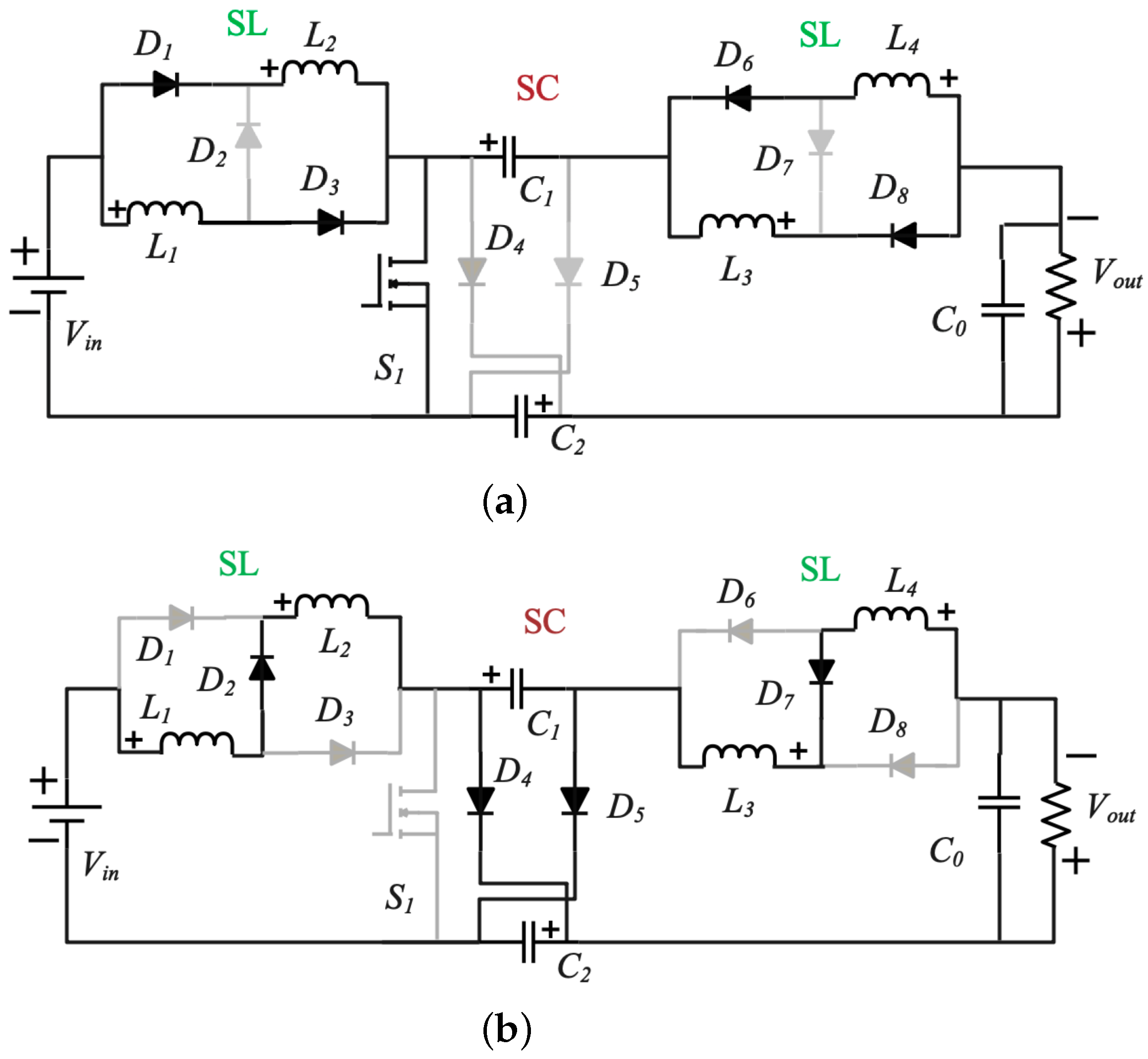
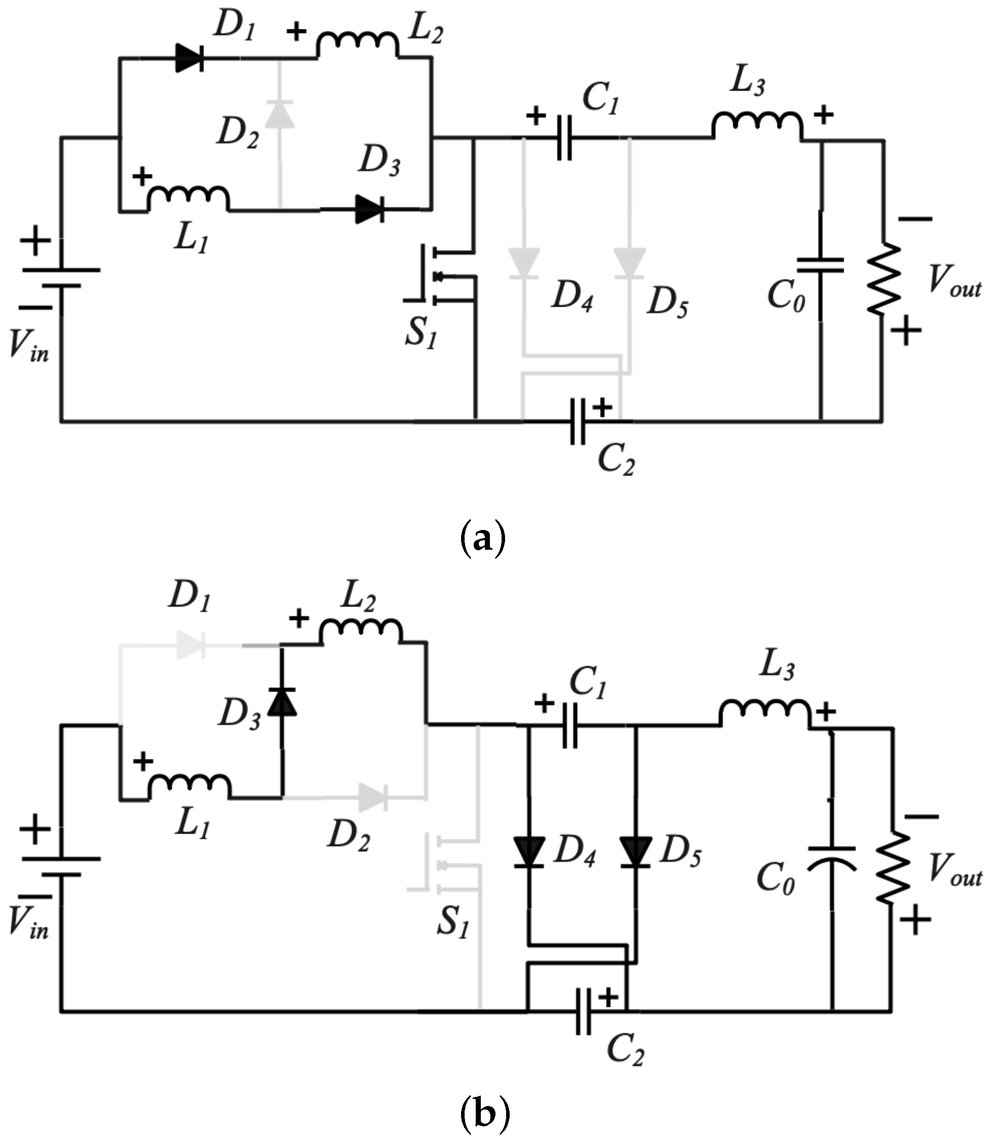
Figure 3 depicts the primary circuit of a conventional Cuk converter. The Cuk converter is utilised for power factor correction applications and has two inductors and two capacitors, which means it has fewer switching losses. The Cuk converter delivers more or less output voltage than the supply voltage with reversed polarity. The inductor L 1 acts as a filter, and the C 1 capacitor decides the extent of energy transfer to the inductor L 1 . The load side inductor and capacitor are responsible for extra circuit requirements with less noise, high transient response, and minimised electromagnetic interference. A Cuk converter is a DC-to-DC converter with a negative capacitive output which is like a buck-boost converter. The difference is that the Cuk converter uses a capacitor instead of an inductor for power transfer and energy storage [27]. The input voltage polarity is reversed for the output voltage of the Cuk converter. If linked properly, this converter generates free ripple output that can be useful for various applications [28]. Different circuit topologies of the converter are introduced depending on the Cuk converters in [29]. The effectiveness of the redesigned Cuk converter has been greatly enhanced. This converter is recommended for the excellent bidirectional operation to manage current and voltage [30].
Within closed-loop systems and fuzzy-logic controllers, several control strategies, e.g., sliding-mode control and traditional proportional-integral (PI) are used to adjust the output voltage [31]. High temperatures affect solar power generation, which is not considered in this study. This study mainly aims to study different topologies of the Cuk converter. This converter is employed in the installation of BLDC motor drives and in PWM.

4.1. Topology-1

This topology is obtained by connecting a switched-inductor (SL) unit with the input side inductor and a switched-capacitor (SC) unit to transfer the energy capacitor. The power circuit schematic of this converter is depicted in Figure 4. Compared to the conventional Cuk prototype, the suggested circuit includes one capacitor, one inductor, and four diodes.
Figure 5a shows the current directions when the switch is turned on (conducting). Through diodes D 1 and D 2 , and switch S 1 , source voltage V i n charges inductors L 1 and L 2 in parallel. During this mode, reversed biased diodes are diodes D 2 , D 4 , and D 5 and inductor L 3 charged by input voltage through switch, capacitor C 1 and C 2 . As both L 1 and L 2 inductors are the same, so the current flowing through them is the same. Figure 5b shows the current direction when the switch is turned off (not conducting). Parallel connected capacitors C 1 and C 2 are charged by the series connection of inductor L 1 and L 2 and input voltage V i n . Similarly, the energy discharge by inductor L 3 also charges the capacitors C 1 and C 2 and provides power to load R. During this mode, reverse biased diodes are diodes D 1 and D 3 .

Design Analysis of Topology-1
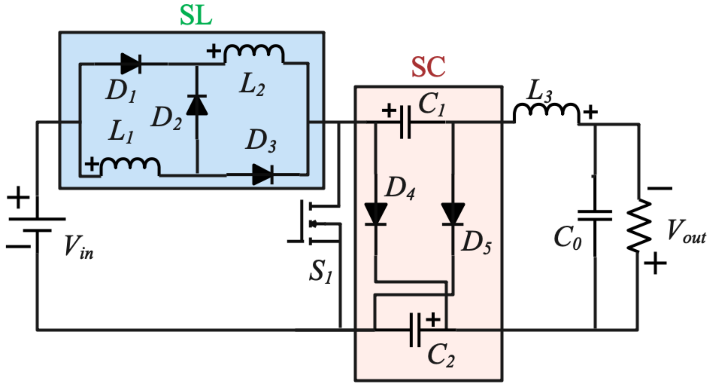
A steady-state analysis of the suggested topology 1 is presented by considering the components are ideal. The source supplies pure DC input voltage V i n , and capacitors have a ripple-free voltage. When the switch S 1 is turned ON, the voltages for the inductors are given as:
V L 1 = V L 2 = V i n
V L 3 = 2 V C V o u t
where, V C = V C 1 = V C 2 . When switch S 1 is turned off the voltages for inductors are given as:
V L 1 = V L 2 = V i n V C 2
V L 3 = V C V o u t
Applying the volt-second method:
V i n D + V i n V C 2 ( 1 D ) = 0
( 2 V C V o u t ) D + ( V C V o u t ) ( 1 D ) = 0
The voltage gain is given by,
G = V o u t V i n = I i n I o u t = ( 1 + D ) 2 1 D
The expression of voltage across switch, capacitors C 1 , C 2 , and reverse voltage across diodes ( D 1 D 5 ) are given in Table 1.

4.2. Topology-2

This topology is obtained by connecting a switched-inductor (SL) unit with the output side inductor and a switched-capacitor (SC) unit to transfer the energy capacitor. The power circuit of this converter is depicted in Figure 6. Compared to the conventional Cuk prototype, the suggested circuit includes one capacitor, one inductor, and four diodes.
Figure 7a shows the equivalent circuit when the switch is turned ON (conducting). The inductor L 1 is charged by source voltage V i n through switch S 1 . Parallel connected inductors L 2 and inductor L 3 are charged through the switch, diodes D 3 and D 5 by capacitors C 1 , C 2 and source voltage V i n . As inductors L 2 and L 3 are the same, the current flowing through them is also the same. During this mode, reversed biased diodes are diode D 1 , D 2 and D 4 . Figure 7b shows the equivalent circuit when the switch is turned OFF (not conducting). Inductors L 1 and source voltage V i n charge parallel-connected capacitors C 1 and C 2 . Similarly, energy discharge by inductors L 2 and L 3 also charges the capacitors C 1 and C 2 and supplies power to load. During this mode, reversed biased diodes are diodes D 3 and D 5 .

Design Analysis of Topology-2
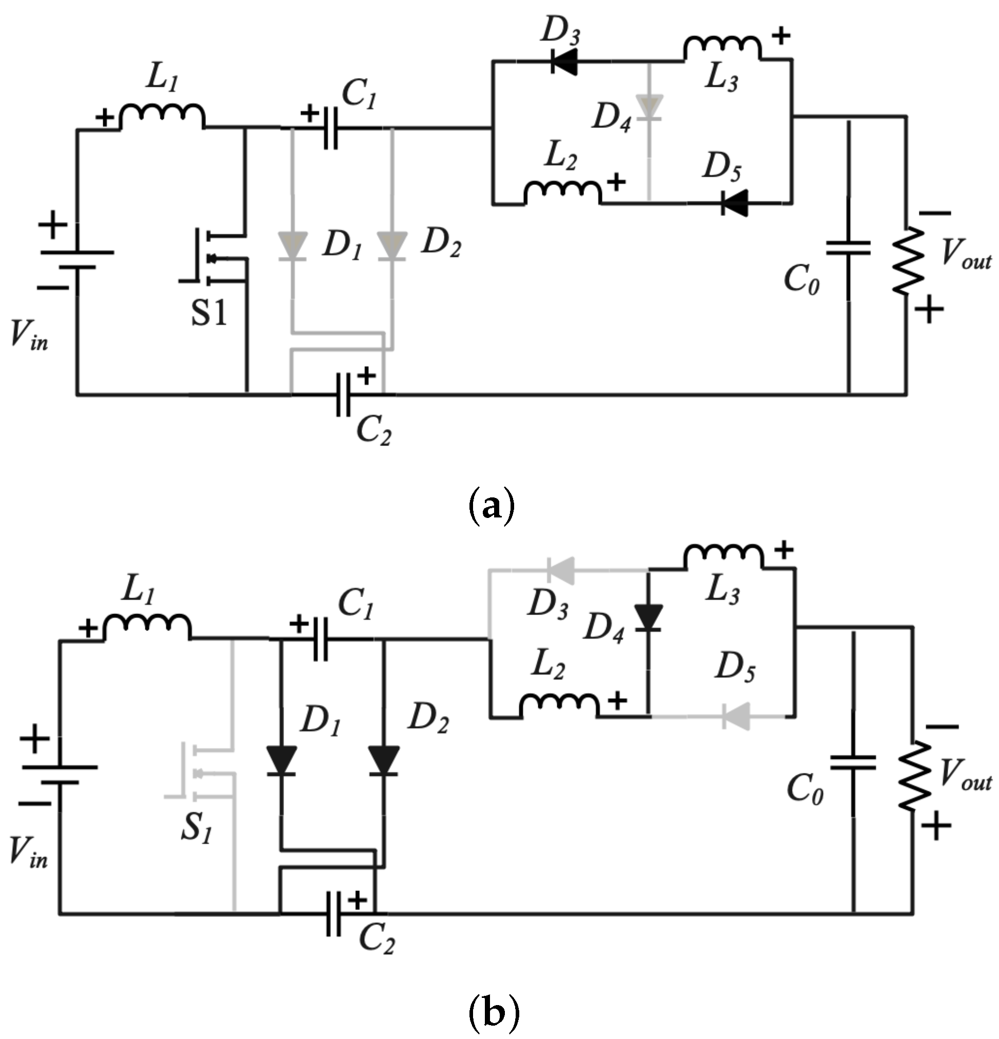
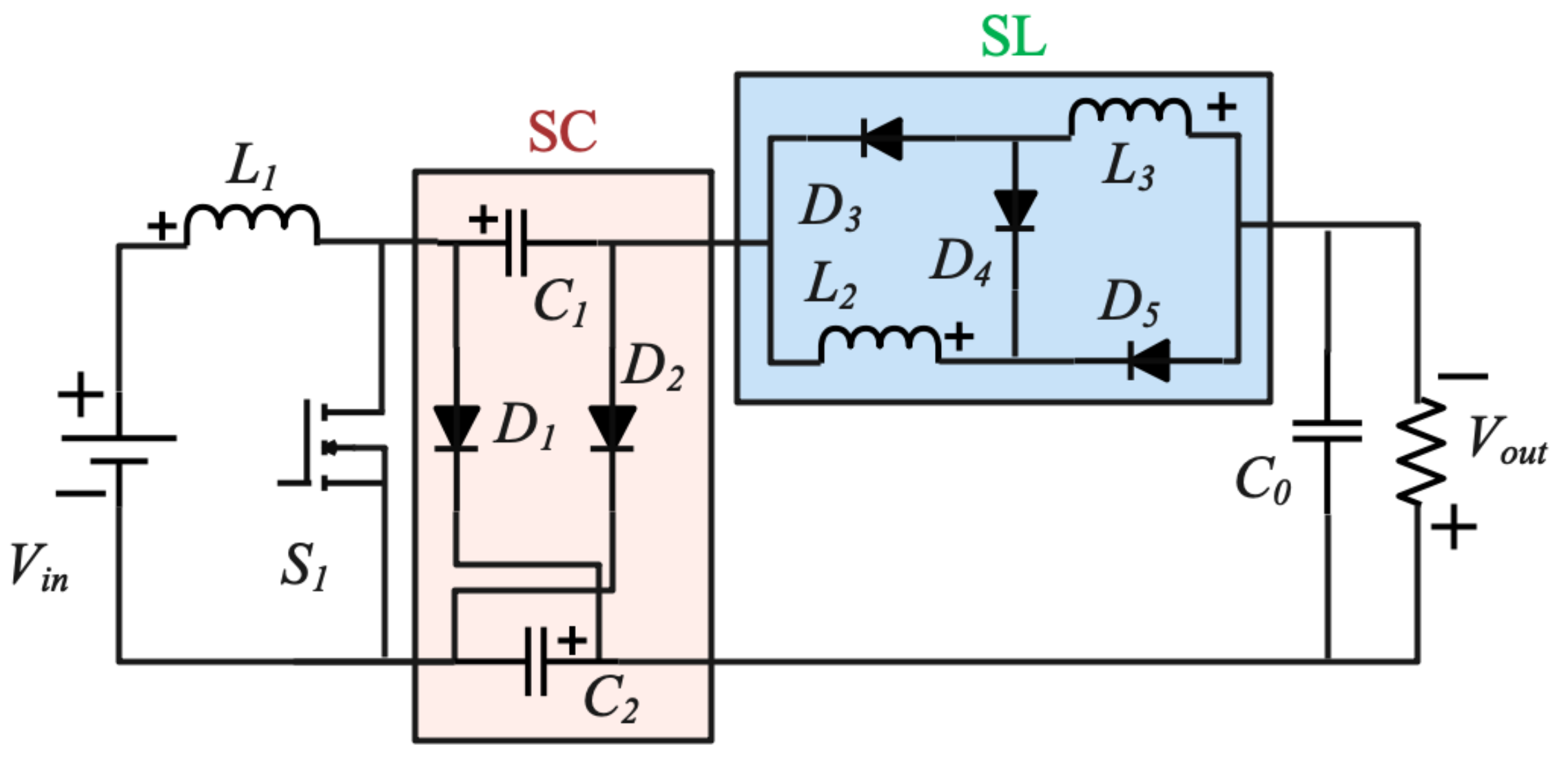
When the switch S 1 is turned ON, the voltages for the inductors are given as:
V L 1 = V i n
V L 2 = V L 3 = 2 V C V o u t
where, V C = V C 1 = V C 2 . When switch S 1 is turned off the voltages for the inductors are given as:
V L 1 = V i n V C
V L 2 = V L 3 = V C V o u t 2
Applying the volt-second method:
V i n D + ( V i n V C ) ( 1 D ) = 0
( 2 V C V o u t ) D + ( V C V o u t 2 ) ( 1 D ) = 0
The voltage gain is given by,
G = V o u t V i n = I i n I o u t = ( 1 + 3 D ) ( 1 + D ) ( 1 D )
The expression of voltage across switch, capacitor C 1 , capacitor C 2 , and reverse voltage across diodes ( D 1 D 5 ) are given in Table 2.

4.3. Topology-3

This topology is obtained by connecting an SL unit in place of both the input side and the output side inductor and an SC unit in place of the transferring energy capacitor. The power circuit for this converter is depicted in Figure 8. Compared to the conventional Cuk prototype, the suggested circuit includes two capacitors, two inductors and seven diodes.
Figure 9a shows the equivalent circuit when the switch is turned ON (conducting). Source voltage V i n charges parallel connected inductors L 1 and L 2 through the switch, diodes D 1 and D 3 . Parallel connected inductors L 3 and L 4 supply power to load through diodes D 6 and D 8 and switch by the help of capacitor C 1 and C 2 . During this mode, reversed biased diodes are diode D 2 , D 4 , D 5 and D 7 . As inductors L 1 and L 2 are the same, an equal amount of current flows through them. Similarly, inductors L 3 and L 4 are the same; an equal amount of current flows through them. Figure 9b shows the current direction when the switch is turned OFF (not conducting). Parallel connected capacitors C 1 and C 2 are charged by source voltage V i n , inductors L 1 and L 2 . Similarly, energy discharge by inductors L 3 and L 4 also charge the capacitors C 1 and C 2 , and also provide power to load. During this mode, reversed biased diodes are diodes D 1 , D 3 , D 6 and D 8 .

Design Analysis of Topology-3

When the switch S 1 is turned ON, the voltages for inductors are given as:
V L 1 = V L 2 = V i n
V L 3 = V L 4 = 2 V C V o u t
where, V C = V C 1 = V C 2 . When switch S 1 is turned off the voltages for the inductors are given as:
V L 1 = V L 1 = V i n V C 2
V L 3 = V L 4 = V C V o u t 2
Applying the volt-second method:
V i n D + ( V i n V C 2 ) ( 1 D ) = 0
( 2 V C V o u t 2 ) D + ( V C V o u t 2 ) ( 1 D ) = 0
The voltage gain is given by,
G = V o u t V i n = I i n I o u t = ( 1 + 3 D ) ( 1 D )
The expression of voltage across switch, capacitor C 1 and C 2 and reverse voltage across diodes ( D 1 D 8 ) are given in Table 3.

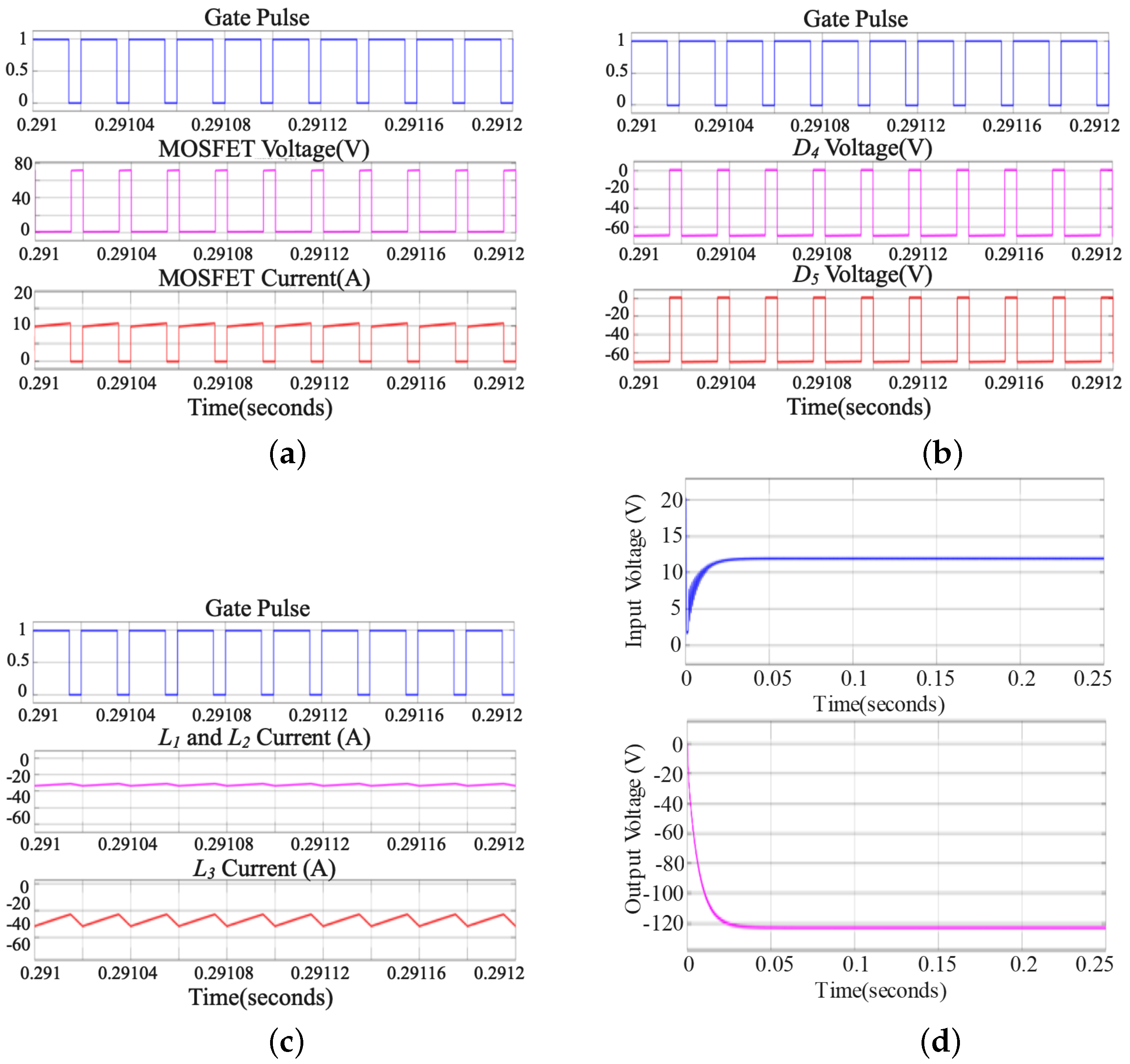
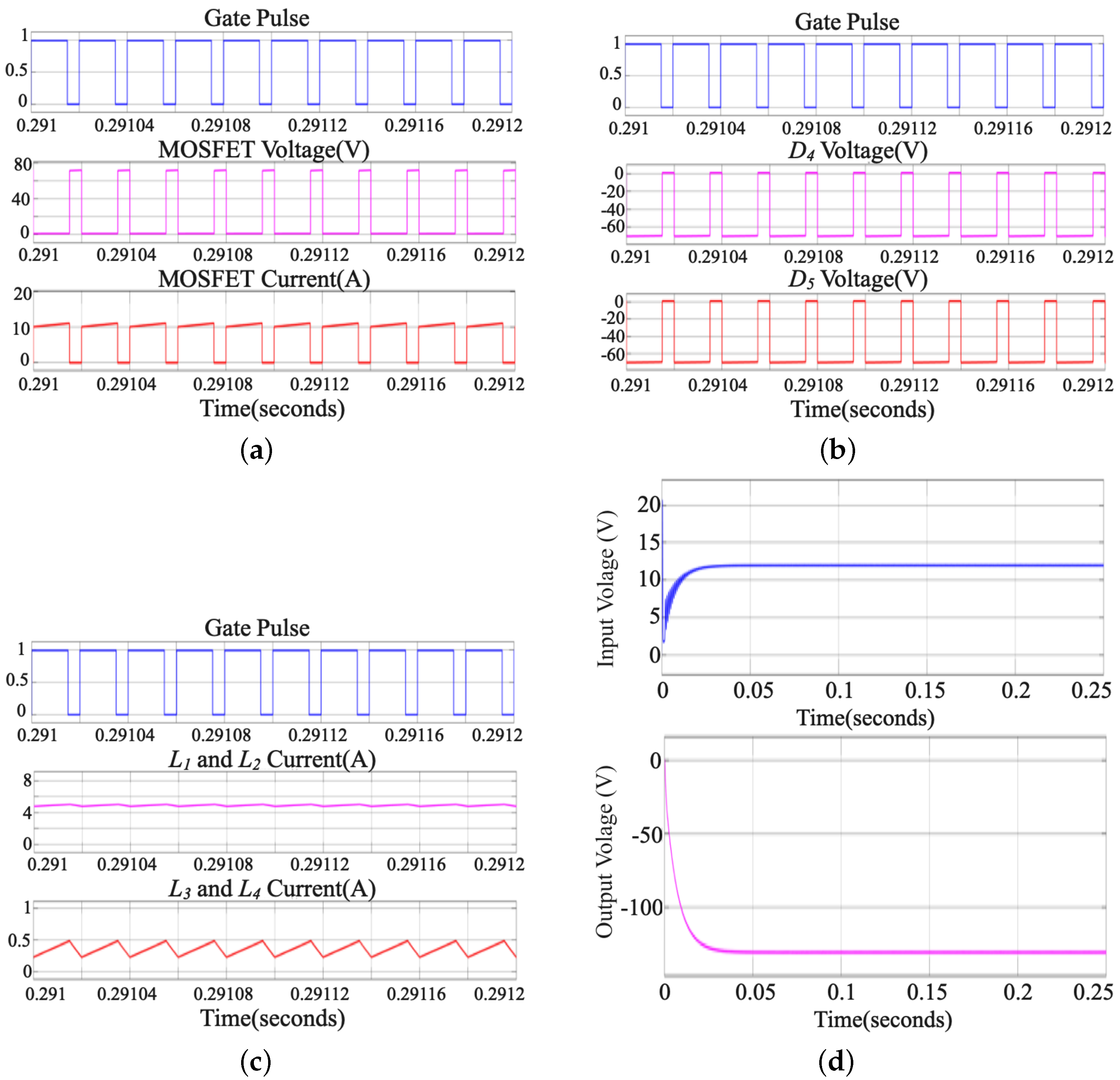
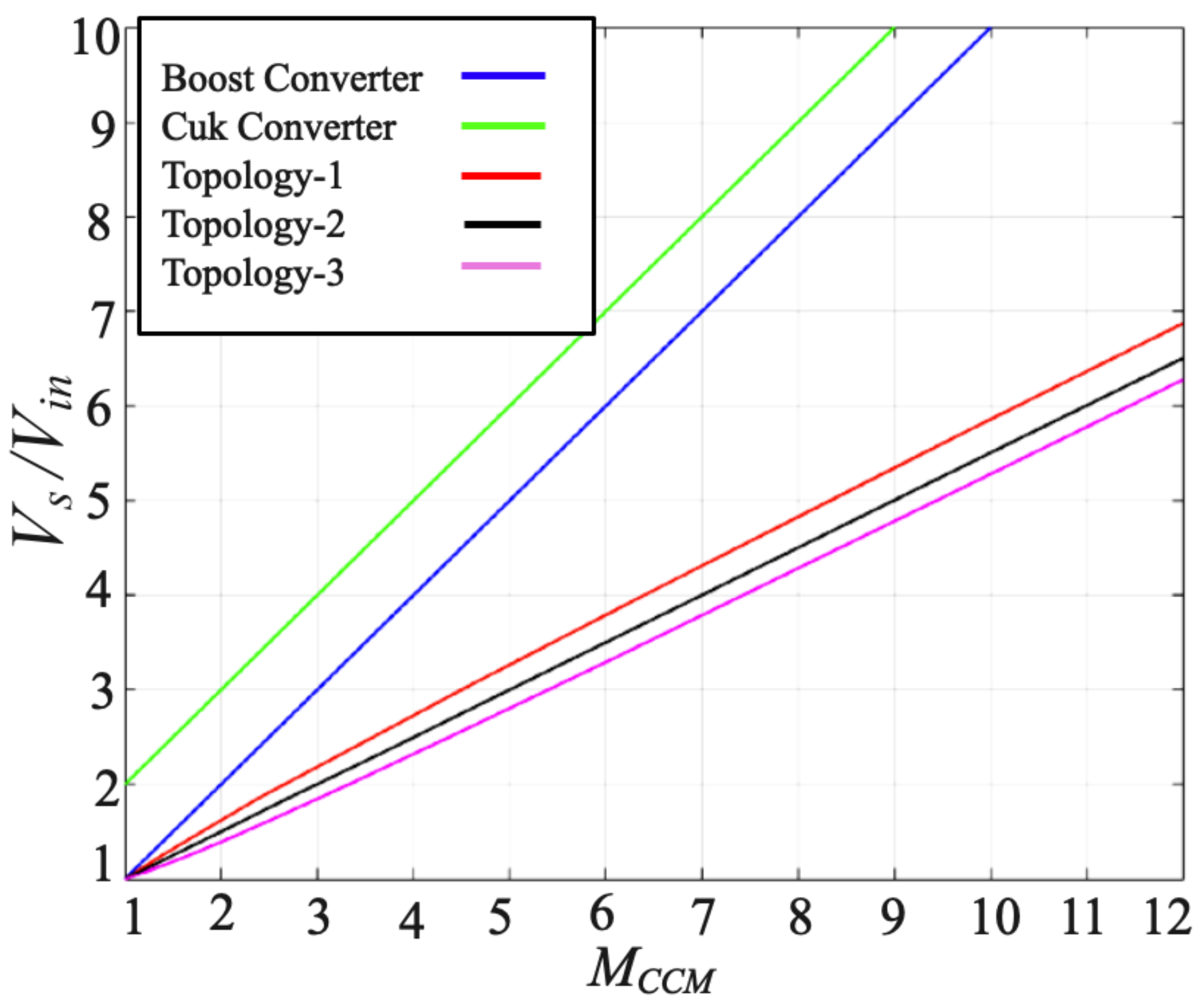
5. Simulation Results and Analysis

The suggested three converters were simulated in the MATLAB Simulink environment to analyze their performance and characteristics. The values of various parameters used for the simulation of these converters are illustrated in Table 4. These converters were simulated using a PV system as an input power source. The PV system was attached with a converter using a coupling capacitor.
The results obtained from topology 1 are presented in Figure 10. Figure 10a depicts the current stress and voltage stress on MOSFET S 1 . Figure 10b depicts the voltage stress on the SC’s two diodes D 4 and D 5 . Figure 10c depicts the current waveform of inductors L 1 , L 2 and L 3 . When MOSFET S 1 is turned ON, the three inductors are charged and discharged when MOSFET S 1 is turned OFF. Figure 10d depicts the input voltage and output voltage waveforms of the converter.
The results obtained from topology 2 are presented in Figure 11. Figure 11a depicts the current stress and voltage stress on MOSFET S 1 . Figure 11b depicts the voltage stress on SC’s two diodes D 1 and D 2 . Figure 11c depicts the current waveform of inductors L 1 , L 2 and L 3 . When MOSFET S 1 is turned ON, the three inductors are charged and discharged when MOSFET S 1 is turned off. Figure 11d depicts the input voltage and output voltage waveforms of the converter.
The results obtained from topology 3 are presented in Figure 12. Figure 12a depicts the current stress and voltage stress on MOSFET S 1 . Figure 12b depicts the voltage stress on the SC’s two diodes D 4 and D 5 . Figure 12c depicts the current waveform of inductors L 1 , L 2 , L 3 and L 4 . When MOSFET S 1 is turned on, the four inductors are charged and discharged when MOSFET S 1 is turned off. Figure 12d depicts the input voltage and output voltage waveform of the converter.
The number of components required for designing the three topologies of the SLSC Cuk converter and voltage gain formula is shown in Table 5. The comparative study of the voltage gain and normalized switch voltage stress for the three topologies of the SLSC Cuk converter with the conventional Cuk converter and boost converter is shown in Figure 13 and Figure 14, respectively. It can be seen that the proposed converter topologies have higher gain than the conventional boost and Cuk converters. Out of the proposed three topologies, topology-3 has the highest gain, which can be seen in Figure 13. From Figure 14, it is concluded that conventional boost and Cuk converters have the highest normalised voltage stress compared to proposed converters.

6. Conclusions

In this study, the topologies of SLSC Cuk converters with low active switch strain and significant voltage gain were successfully designed. The continuous conduction mode operation of the converters was investigated. The suggested converters were controlled at a constant frequency using the PWM approach. The proposed converters were compared with traditional Cuk and boost converters. The suggested converters have several advantages, including low voltage stress and high voltage gain, which allow for selecting an active switch, a lesser voltage rating and low on-state resistance, continuous output and input currents, single switch operation, ease of design, and high efficiency. These converters were simulated with a 12 V PV source as an input of the converter on the MATLAB/Simulink platform. The current stress on the MOSFET switch of three topologies was 10 A. The voltage stress on the MOSFET switch of topology-1 and topology-3 was 78 V, while for topology-2, it was 46 V. Among these topologies, topology-2 provided the least voltage gain, while topology-3 provided the highest voltage gain. The hardware implementation can be considered for future study.

Author Contributions

Conceptualization, N.P., M.S.B., M.S. and D.K.D.; methodology, N.P. and F.A.; software, N.P., F.A., M.S. and D.K.D.; validation, N.P., M.S.B., I.B.M.T. and M.G.H.; formal analysis, N.P., M.S.B., F.A., I.B.M.T. and M.G.H.; investigation, N.P. and M.S.B.; resources, N.P. and M.S.B.; writing, N.P., F.A., M.S. and D.K.D.; writing, review and editing, M.S.B., I.B.M.T. and M.G.H.; visualization, M.S.B.; supervision, N.P. and M.S.B.; project administration, N.P., I.B.M.T. and M.G.H.; funding, I.B.M.T. and M.G.H. All authors have read and agreed to the published version of the manuscript.

Funding

This research was funded by the Taif University Researchers Supporting Project, grant number TURSP-2020/61.

Institutional Review Board Statement

Not applicable.

Informed Consent Statement

Not applicable.

Data Availability Statement

All data generated or analyzed during this study are included in this published article.

Acknowledgments

The authors would like to acknowledge the financial support received from the Taif University Researchers Supporting Project Number (TURSP-2020/61), Taif University, Taif, Saudi Arabia.

Conflicts of Interest

The authors declare no conflict of interest.

References

  1. Khireddine, M.; Makhloufi, M.; Abdessemed, Y.; Boutarfa, A. Tracking power photovoltaic system with a fuzzy logic control strategy. In Proceedings of the 2014 6th International Conference on Computer Science and Information Technology (CSIT), Amman, Jordan, 26–27 March 2014; pp. 42–49. [Google Scholar]
  2. Ranjana, M.S.B.; Reddy, N.S.; Kumar, R.K.P. Non-isolated dual output hybrid DC-DC multilevel converter for photovoltaic applications. In Proceedings of the 2014 2nd International Conference on Devices, Circuits and Systems (ICDCS), Coimbatore, India, 6–8 March 2014; pp. 1–6. [Google Scholar]
  3. Musale, A.S.; Deshmukh, B.T. Three level DC-DC boost converter for high conversion ratio. In Proceedings of the 2016 International Conference on Electrical, Electronics, and Optimization Techniques (ICEEOT), Chennai, India, 3–5 March 2016; pp. 643–647. [Google Scholar]
  4. Almalaq, Y.; Alateeq, A.; Matin, M. Silicon carbide DC-DC multilevel Cuk converter. In Wide Bandgap Power Devices and Applications; International Society for Optics and Photonics: Bellingham, DC, USA, 2016; Volume 9957, p. 99570I. [Google Scholar]
  5. Li, W.; Lv, X.; Deng, Y.; Liu, J.; He, X. A review of non-isolated high step-up DC/DC converters in renewable energy applications. In Proceedings of the 2009 Twenty-Fourth Annual IEEE Applied Power Electronics Conference and Exposition, Washington, DC, USA, 15–19 February 2009; pp. 364–369. [Google Scholar]
  6. Forouzesh, M.; Siwakoti, Y.P.; Gorji, S.A.; Blaabjerg, F.; Lehman, B. Step-up DC–DC converters: A comprehensive review of voltage-boosting techniques, topologies, and applications. IEEE Trans. Power Electron. 2017, 32, 9143–9178. [Google Scholar] [CrossRef]
  7. Moradpour, R.; Ardi, H.; Tavakoli, A. Design and implementation of a new SEPIC-based high step-up DC/DC converter for renewable energy applications. IEEE Trans. Ind. Electron. 2017, 65, 1290–1297. [Google Scholar] [CrossRef]
  8. Hsieh, Y.P.; Chen, J.F.; Liang, T.J.P.; Yang, L.S. Novel high step-up DC–DC converter with coupled-inductor and switched-capacitor techniques for a sustainable energy system. IEEE Trans. Power Electron. 2011, 26, 3481–3490. [Google Scholar] [CrossRef]
  9. Choi, B.H.; Lee, S.W.; Thai, V.; Rim, C.T. A novel single-SiC-switch-based ZVZCS tapped boost converter. IEEE Trans. Power Electron. 2013, 29, 5181–5194. [Google Scholar] [CrossRef]
  10. Salehi, S.M.; Dehghan, S.M.; Hasanzadeh, S. Interleaved-input series-output ultra-high voltage gain DC–DC converter. IEEE Trans. Power Electron. 2018, 34, 3397–3406. [Google Scholar] [CrossRef]
  11. Ardi, H.; Ajami, A.; Sabahi, M. A novel high step-up DC–DC converter with continuous input current integrating coupled inductor for renewable energy applications. IEEE Trans. Ind. Electron. 2017, 65, 1306–1315. [Google Scholar] [CrossRef]
  12. Heidari, M.; Farzanehfard, H.; Esteki, M. Single-Switch Single-Magnetic Core High Step-up Converter with Continuous Input Current and Reduced Voltage Stress for Photovoltaic Applications. In Proceedings of the 2019 10th International Power Electronics, Drive Systems and Technologies Conference (PEDSTC), Shiraz, Iran, 12–14 February 2019; pp. 695–700. [Google Scholar]
  13. Abbasi, M.; Babaei, E.; Tousi, B. New family of non-isolated step-up/down and step-up switched-capacitor-based DC–DC converters. IET Power Electron. 2019, 12, 1706–1720. [Google Scholar] [CrossRef]
  14. Premkumar, M.; Kumar, C.; Anbarasan, A.; Sowmya, R. A novel non-isolated high step-up DC–DC boost converter using single switch for renewable energy systems. Electr. Eng. 2020, 102, 811–829. [Google Scholar] [CrossRef]
  15. Karimian, F.; Nahavandi, A. Design and analysis of a new structure of non-isolated DC–DC cuk–boost converter with high voltage gain. IET Power Electron. 2019, 12, 530–540. [Google Scholar] [CrossRef]
  16. Chakraborty, S.; Verma, S.; Salgotra, A.; Elavarasan, R.M.; Elangovan, D.; Mihet-Popa, L. Solar-Based DG Allocation Using Harris Hawks Optimization While Considering Practical Aspects. Energies 2021, 14, 5206. [Google Scholar] [CrossRef]
  17. Mahar, A.M.; Shaikh, P.H.; Mahar, A.R.; Memon, Z.A.; Khatri, S.A.; Shah, S.F. Simulation of efficient non-isolated DC-DC boost converter topology for photovoltaic application. AIP Conf. Proc. 2019, 2119, 020019. [Google Scholar]
  18. Saravanan, S.; Babu, N.R. Analysis and implementation of high step-up DC-DC converter for PV based grid application. Appl. Energy 2017, 190, 64–72. [Google Scholar] [CrossRef]
  19. Libra, M.; Petrík, T.; Poulek, V.; Tyukhov, I.I.; Kouřím, P. Changes in the Efficiency of Photovoltaic Energy Conversion in Temperature Range with Extreme Limits. IEEE J. Photovoltaics 2021, 11, 1479–1484. [Google Scholar] [CrossRef]
  20. Poulek, V.; Šafránková, J.; Černá, L.; Libra, M.; Beránek, V.; Finsterle, T.; Hrzina, P. PV panel and PV inverter damages caused by combination of edge delamination, water penetration, and high string voltage in moderate climate. IEEE J. Photovoltaics 2021, 11, 561–565. [Google Scholar] [CrossRef]
  21. Shemelin, V.; Matuska, T. Detailed modeling of flat plate solar collector with vacuum glazing. Int. J. Photoenergy 2017, 2017, 1587592. [Google Scholar] [CrossRef] [Green Version]
  22. Priyadarshi, N.; Padmanaban, S.; Maroti, P.K.; Sharma, A. An extensive practical investigation of FPSO-based MPPT for grid integrated PV system under variable operating conditions with anti-islanding protection. IEEE Syst. J. 2018, 13, 1861–1871. [Google Scholar] [CrossRef] [Green Version]
  23. Priyadarshi, N.; Padmanaban, S.; Bhaskar, M.S.; Blaabjerg, F.; Sharma, A. A fuzzy SVPWM based inverter control realization of grid integrated PV-wind system with FPSO MPPT algorithm for a grid-connected PV/wind power generation system: Hardware implementation. Power Appl. 2018, 12, 962–971. [Google Scholar]
  24. Priyadarshi, N.; Padmanaban, S.; Holm-Nielsen, J.B.; Blaabjerg, F.; Bhaskar, M.S. An experimental estimation of hybrid ANFIS–PSO-based MPPT for PV grid integration under fluctuating sun irradiance. IEEE Syst. J. 2019, 14, 1218–1229. [Google Scholar] [CrossRef]
  25. Priyadarshi, N.; Padmanaban, S.; Bhaskar, M.S.; Blaabjerg, F.; Holm-Nielsen, J.B.; Azam, F.; Sharma, A.K. A hybrid photovoltaic-fuel cell-based single-stage grid integration with Lyapunov control scheme. IEEE Syst. J. 2019, 14, 3334–3342. [Google Scholar] [CrossRef]
  26. Priyadarshi, N.; Bhaskar, M.S.; Padmanaban, S.; Blaabjerg, F.; Azam, F. New CUK–SEPIC converter based photovoltaic power system with hybrid GSA–PSO algorithm employing MPPT for water pumping applications. IET Power Electron. 2020, 13, 2824–2830. [Google Scholar] [CrossRef]
  27. Singh, M. Power Electronics; Tata McGraw-Hill Education: New York, NY, USA, 2008. [Google Scholar]
  28. Chung, H.H.; Tse, K.; Hui, S.R.; Mok, C.; Ho, M. A novel maximum power point tracking technique for solar panels using a SEPIC or Cuk converter. IEEE Trans. Power Electron. 2003, 18, 717–724. [Google Scholar] [CrossRef]
  29. Zhu, M.; Luo, F.L. Enhanced Self-Lift Ck Converter for Negative-to-Positive Voltage Conversion. IEEE Trans. Power Electron. 2010, 25, 2227–2233. [Google Scholar] [CrossRef]
  30. Su-Won, L.; Lee, S.; Chil-Hwan, J. A New High Efficient Bi-directional DC/DC Converter in the Dual Voltage System. J. Electr. Eng. Technol. 2006, 1, 343–350. [Google Scholar]
  31. Chen, Z. PI and sliding mode control of a Cuk converter. IEEE Trans. Power Electron. 2012, 27, 3695–3703. [Google Scholar] [CrossRef]
Figure 1. PV cell model.
Electronics 11 01381 g001
Figure 2. Hybrid FLC-SMC-based MPPT-controlled PV System.
Electronics 11 01381 g002
Figure 3. Basic CUK converter.
Electronics 11 01381 g003
Figure 4. Topology 1: Power circuit of type-1 switched-inductor-switched-capacitor (SLSC) Cuk converter.
Electronics 11 01381 g004
Figure 5. Topology 1: Operating mode of SLSC CUK converter (a) ON Mode (b) OFF Mode.
Electronics 11 01381 g005
Figure 6. Topology 2: Power circuit of type-2 switched-inductor-switched-capacitor (SLSC) Cuk converter.
Electronics 11 01381 g006
Figure 7. Topology 2: Operating mode of SLSC CUK converter (a) ON Mode (b) OFF Mode.
Electronics 11 01381 g007
Figure 8. Topology 3: Power circuit of type-2 switched-inductor-switched-capacitor (SLSC) Cuk converter.
Electronics 11 01381 g008
Figure 9. Topology 3: Operating mode of SLSC CUK converter (a) ON Mode (b) OFF Mode.
Electronics 11 01381 g009
Figure 10. Simulation results of topology 1: (a) voltage and current of MOSFET (b) voltage across diodes (c) inductor’s current (d) input and output voltage.
Electronics 11 01381 g010
Figure 11. Simulation results of topology 2: (a) voltage and current of MOSFET (b) voltage across diodes (c) inductor’s current (d) input and output voltage.
Electronics 11 01381 g011
Figure 12. Simulation results of topology 3: (a) voltage and current of MOSFET (b) voltage across diodes (c) inductor’s current (d) input and output voltage.
Electronics 11 01381 g012
Figure 13. Comparison of converters in terms of voltage gain.
Electronics 11 01381 g013
Figure 14. Comparison of converters in terms of normalized switch voltage stress.
Electronics 11 01381 g014
Table 1. Equations of voltages for type-1 SLSC CUK converter.
ParametersExpression
Capacitors C 1 and C 2 1 + D 1 D V i n
Switch S 1 1 + D 1 D V i n
Diodes D 1 and D 3 D 1 D V i n
Diodes D 2 V i n
Diodes D 4 and D 5 1 + D 1 D V i n
Table 2. Equations of voltages for type-2 SLSC CUK converter.
ParametersExpression
Capacitors C 1 and C 2 1 1 D V i n
Switch S 1 1 1 D V i n
Diodes D 1 and D 2 1 1 D V i n
Diodes D 3 and D 5 D ( 1 + D ) ( 1 D ) V i n
Diodes D 4 1 1 + D V i n
Table 3. Equations of voltages for type-3 SLSC CUK converter.
ParametersExpression
Capacitors C 1 and C 2 1 + D 1 D V i n
Switch S 1 1 + D 1 D V i n
Diodes D 1 , D 3 , D 6 and D 8 D 1 D V i n
Diodes D 2 and D 7 V i n
Diodes D 4 and D 5 1 + D 1 D V i n
Table 4. Parameter values used for simulation.
ParametersTopology 1Topology 2Topology 3
Input Voltage (in Volts)121212
Switching Frequency (in kHz)555
Inductor (in μ H)600600600
Capacitor (in μ F)222222
Load Resistance (in Ω )19075210
Table 5. Comparison of Converters.
ParameterBoostCukTopology 1Topology 2Topology 3
Diode11558
Capacitors12333
Inductors12334
Switch11111
Voltage Gain 1 1 D V i n D 1 D V i n ( 1 + D ) 2 1 D V i n 1 + 3 D ( 1 + D ) ( 1 D ) V i n 1 + 3 D ( 1 D ) V i n
Publisher’s Note: MDPI stays neutral with regard to jurisdictional claims in published maps and institutional affiliations.

