
Design and Demonstration of a 540 V/28 V SiC-Based Resonant DC–DC Converter for Auxiliary Power Supply in More Electric Aircraft


Abstract
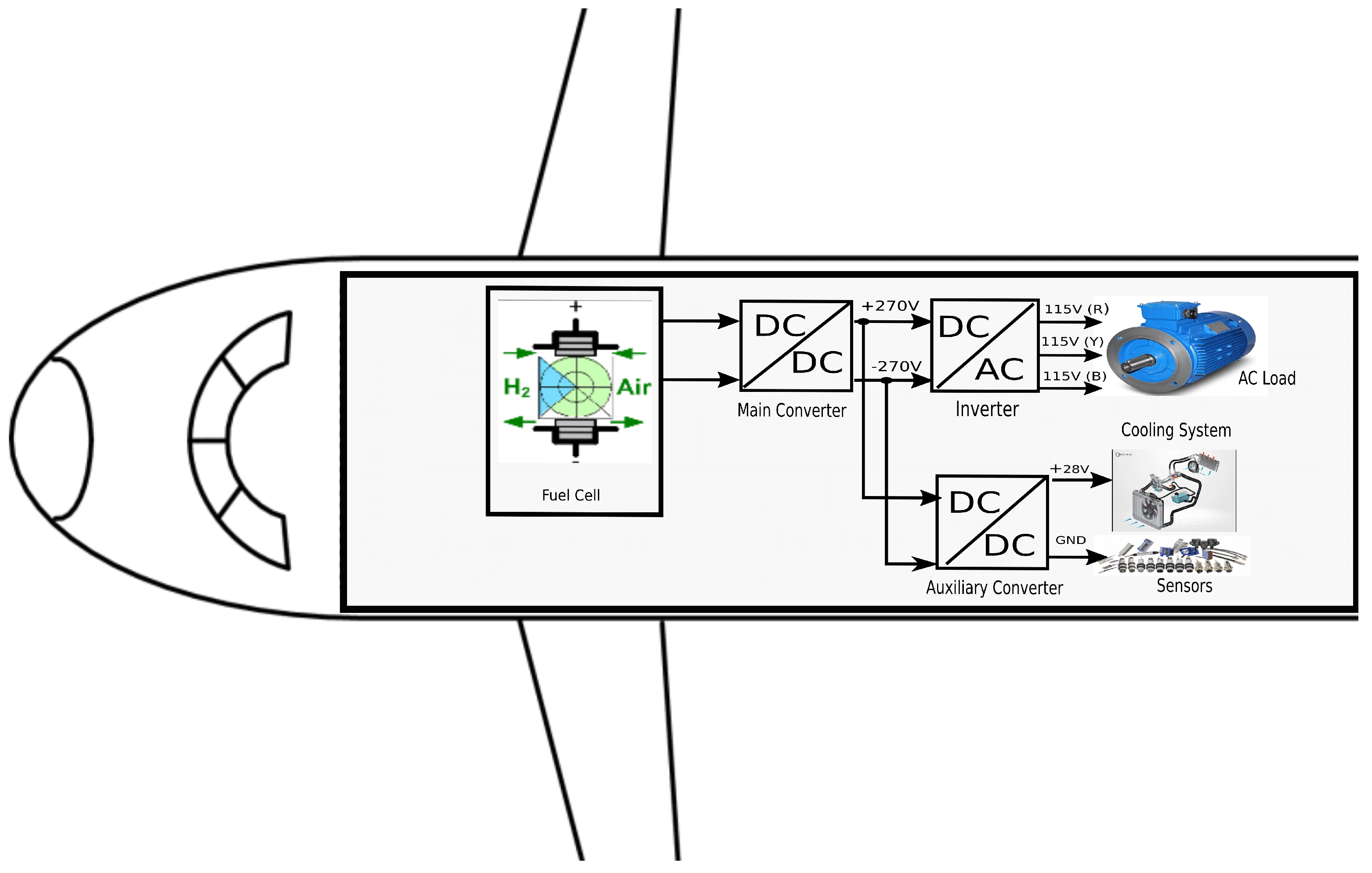
:1. Introduction
- (1)
- High–voltage gain;
- (2)
- High power density with reduction of volume and weight;
- (3)
- High conversion efficiency;
- (4)
- High reliability and redundancy to ensure safe operation even in the event of a system failure;
- (5)
- MIL–STD–704F (aircraft electric power characteristics) compliance for voltage regulation on the ±270 V dc–bus.
2. Operation Principle
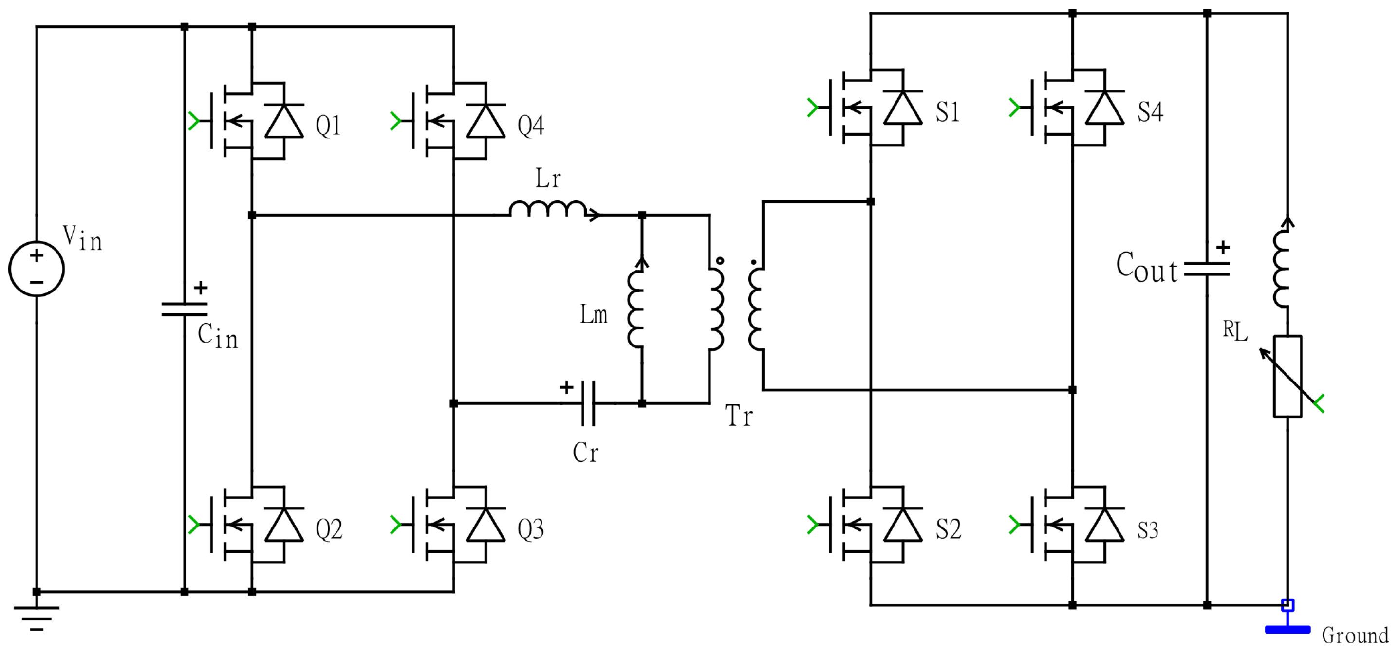
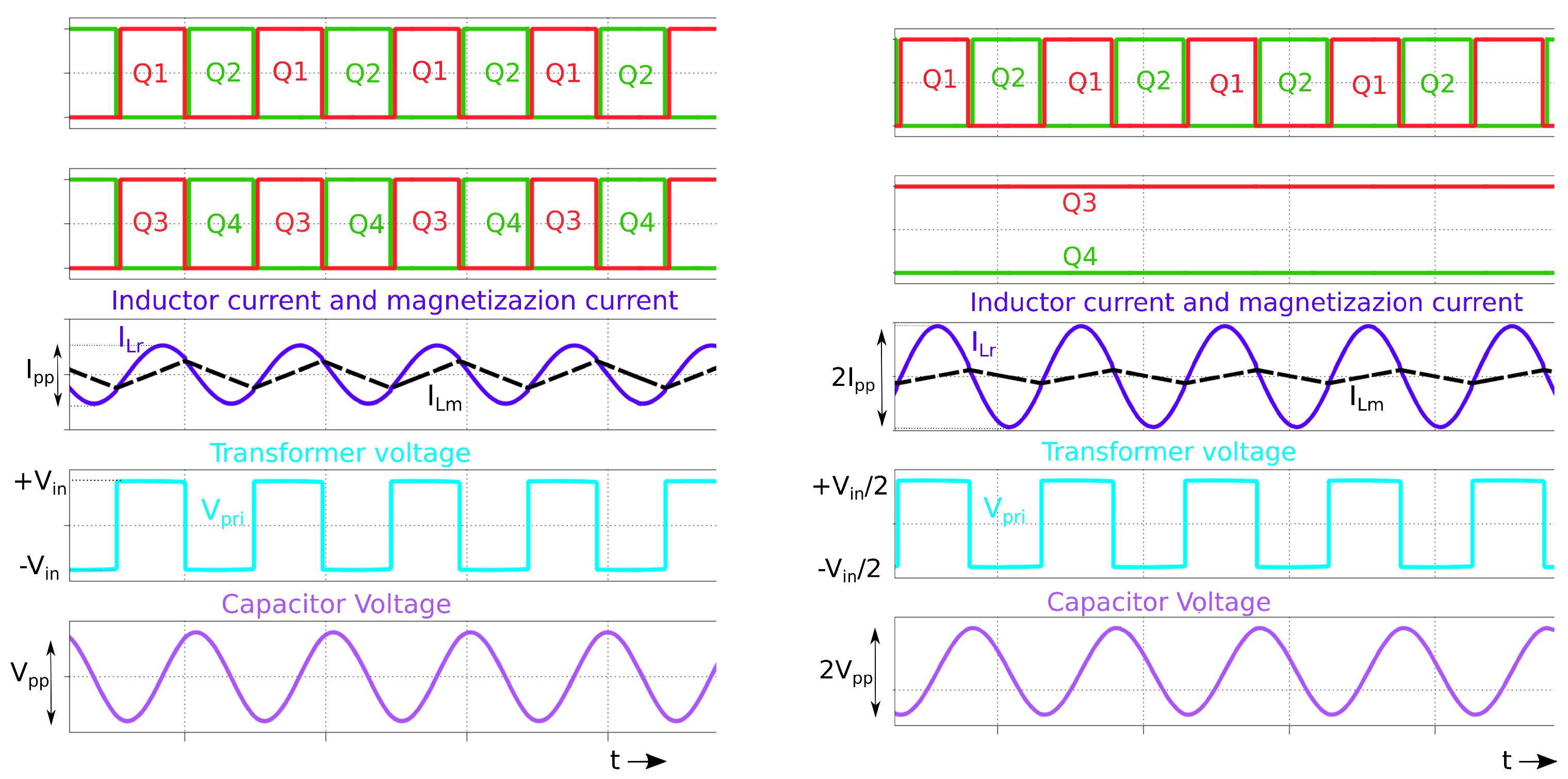
2.1. Synchronous Full–Bridge LLC Converter
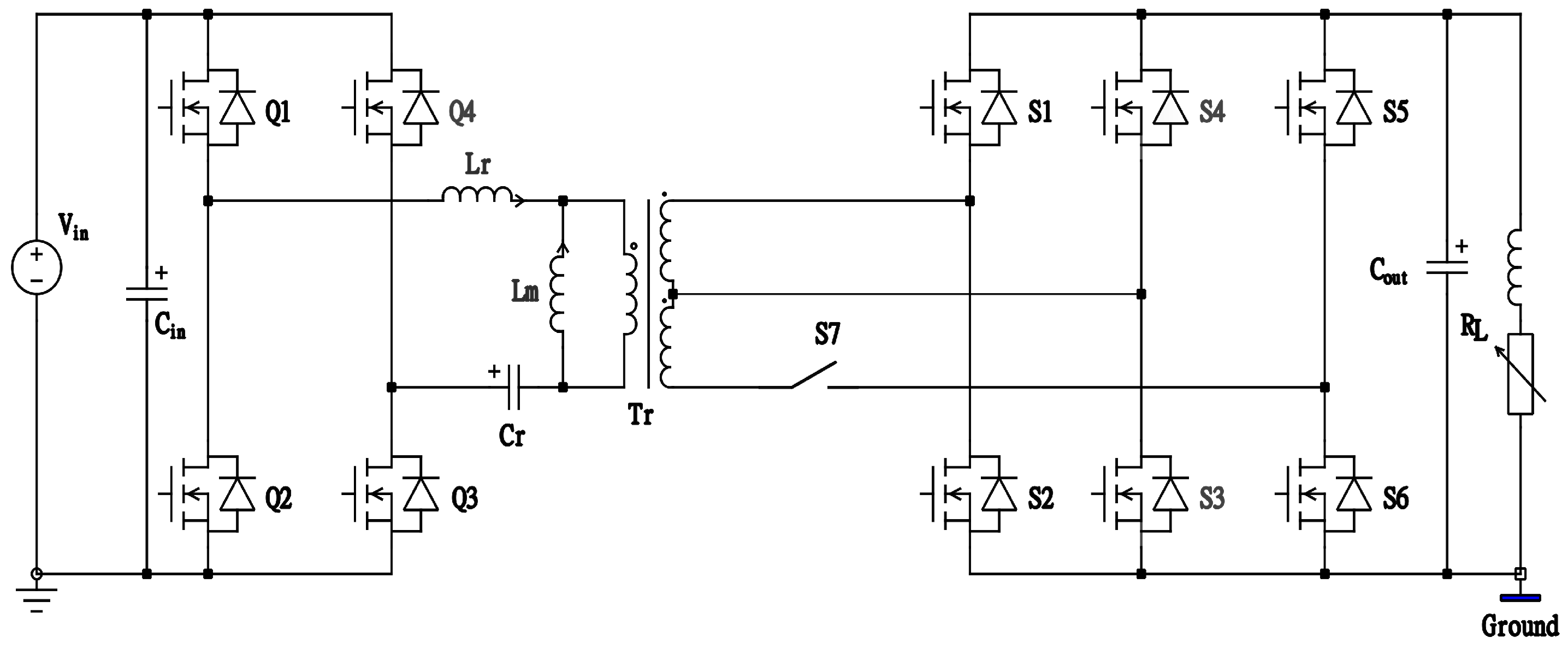
2.2. Proposed Converter
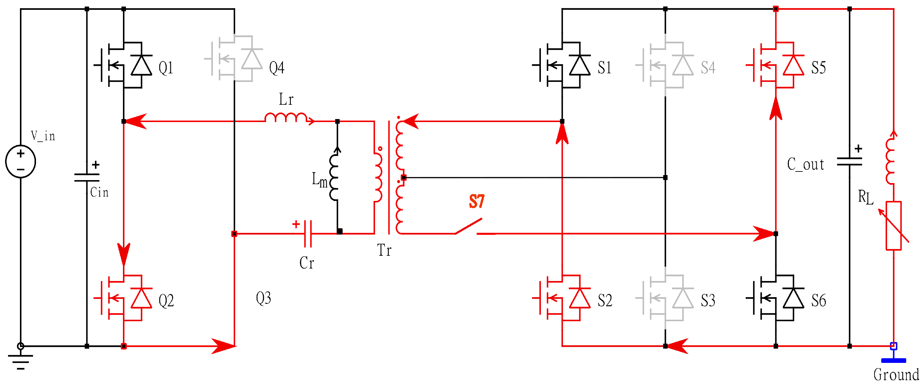
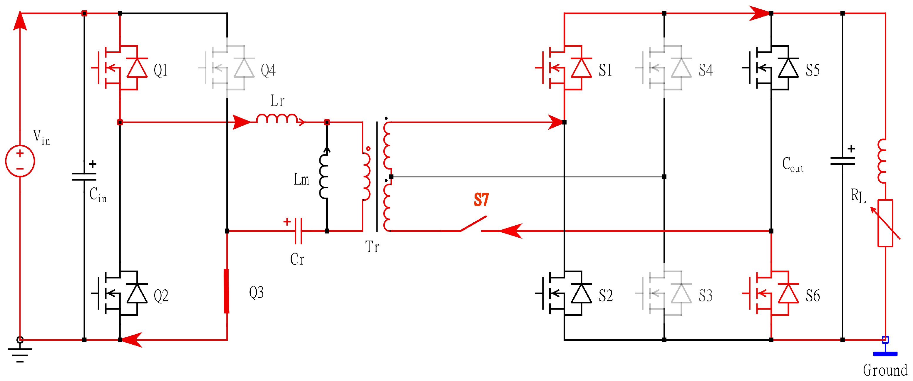
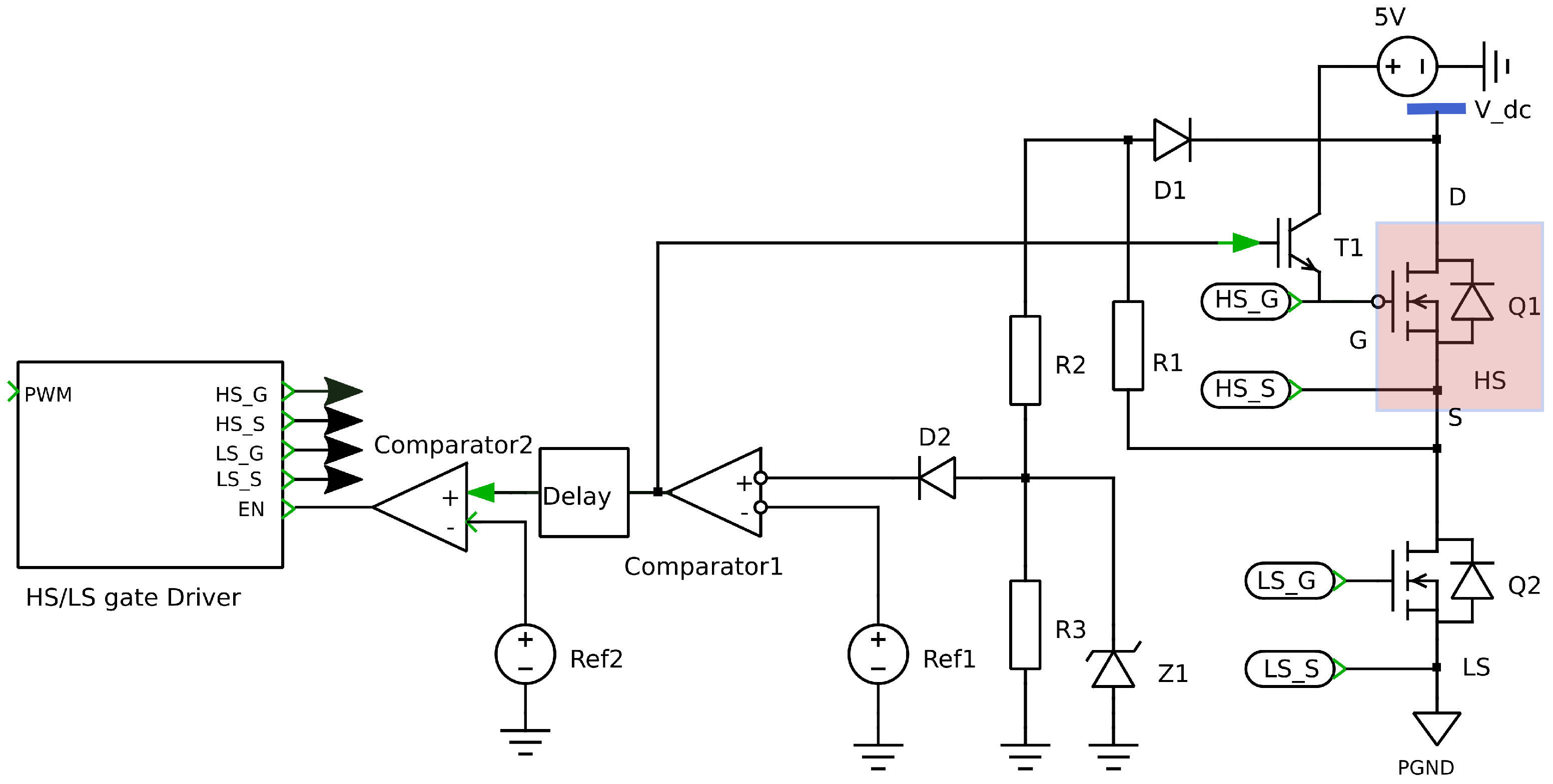
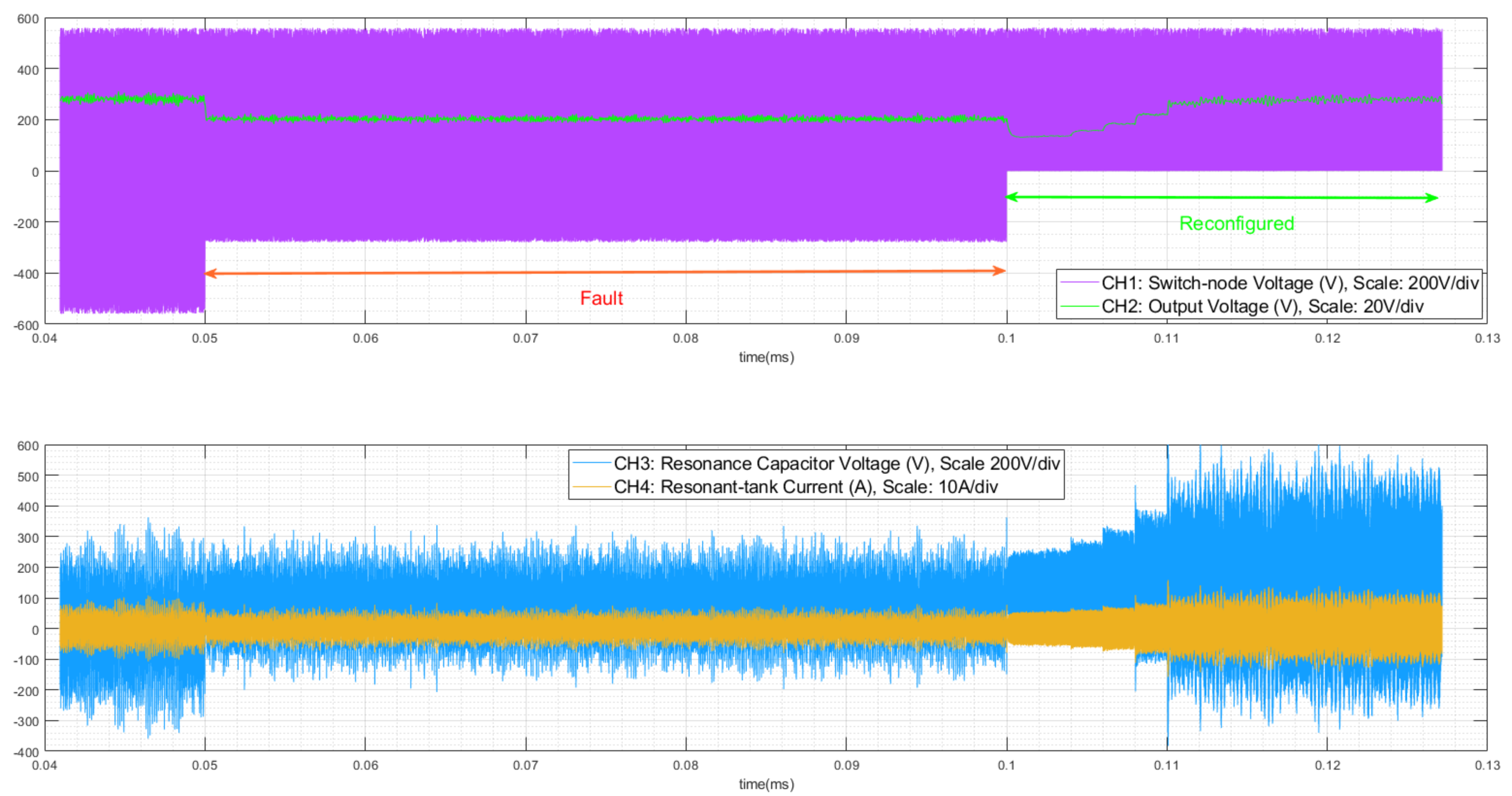
2.3. Operation under Fault
- To reconfigure the primary side of the converter to an HB, the switch Q4 is open–circuited permanently. Since Q3 is permanently short–circuited, the switch Q3 is henceforward assumed as a permanent short–circuited path and utilized as part of the current commutation path as a closed link.
- Simultaneously, in the secondary bridge, the switch S7 is turned on continuously, and the bottom node of the transformer is connected to the middle node of the switch–pair S5, S6. Since the switches S4 and S3 are no longer part of the rectification circuit, they are deliberately left open–circuited by turning their respective gate signals off and are unused for the duration of this mode.
- Since S5 and S6 are available in the secondary rectification path, S1, S6, and S5, S2 are switched in a complementary fashion to achieve a synchronous rectification. Note that by choosing this configuration, both the secondary and the tertiary windings of the transformer are energized.
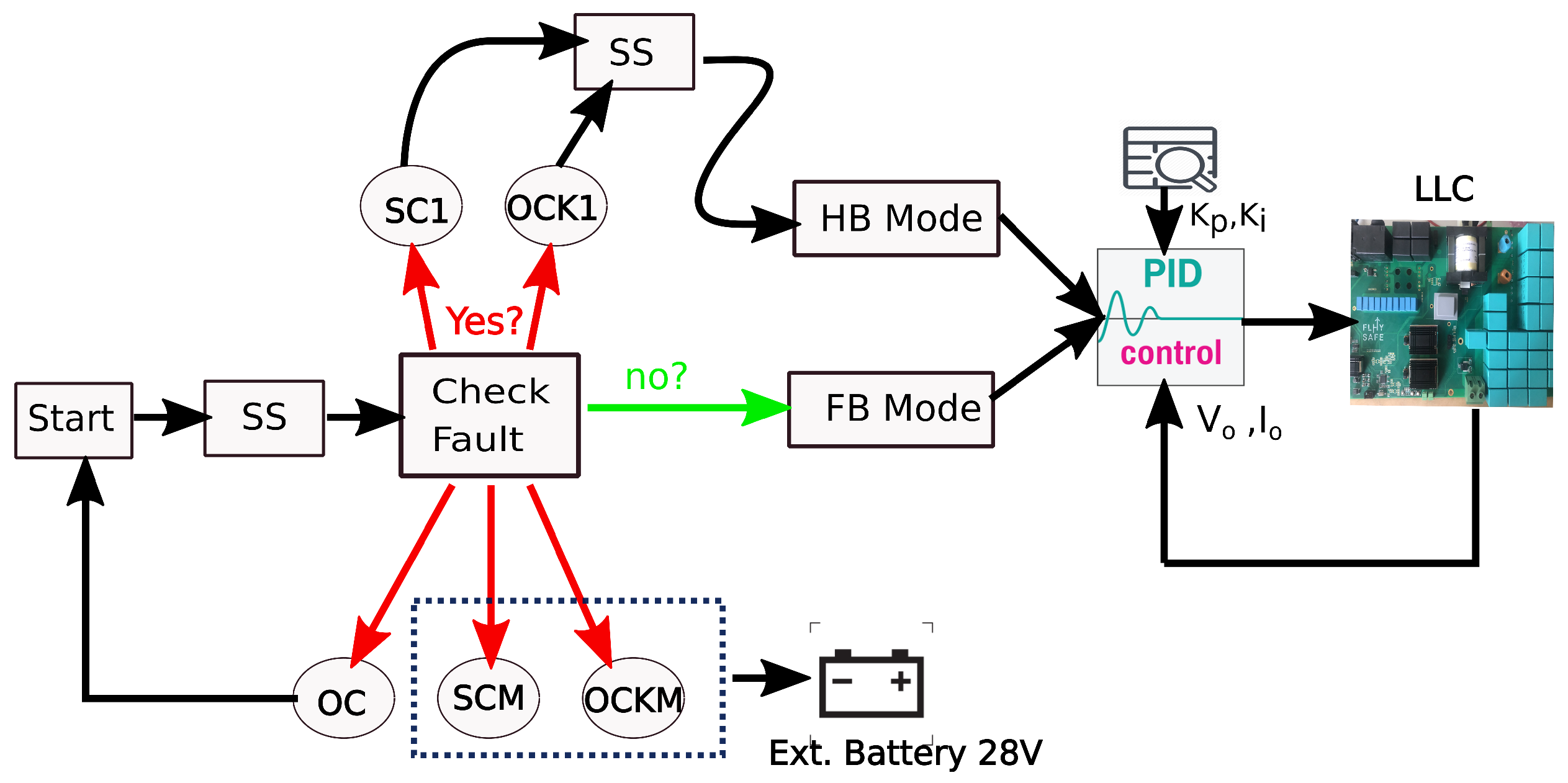
2.4. Fault Detection Mechanism
3. Converter Design
3.1. Resonant Stage Design
- The first step is to obtain the turns ratio of the transformer. The turns ratio of the transformer depends on the nominal input voltage (Vin,nom), output voltage (Vo), forward MOSFET voltage drop (VDS,on), and the diode forward voltage drop (Vf) and can be obtained from Equation (1).
- Alongside, the maximum voltage gain (Mmax) and minimum voltage gain (Mmin) are to be determined. The voltage gain is the ratio of output voltage and input voltage, and is not a fixed value, if the input voltage of the converter fluctuates. These two parameters are calculated based on design constraints based on Equation (2):In order to deal with overload capacities of the converter, a safety factor of 1.2 is considered.
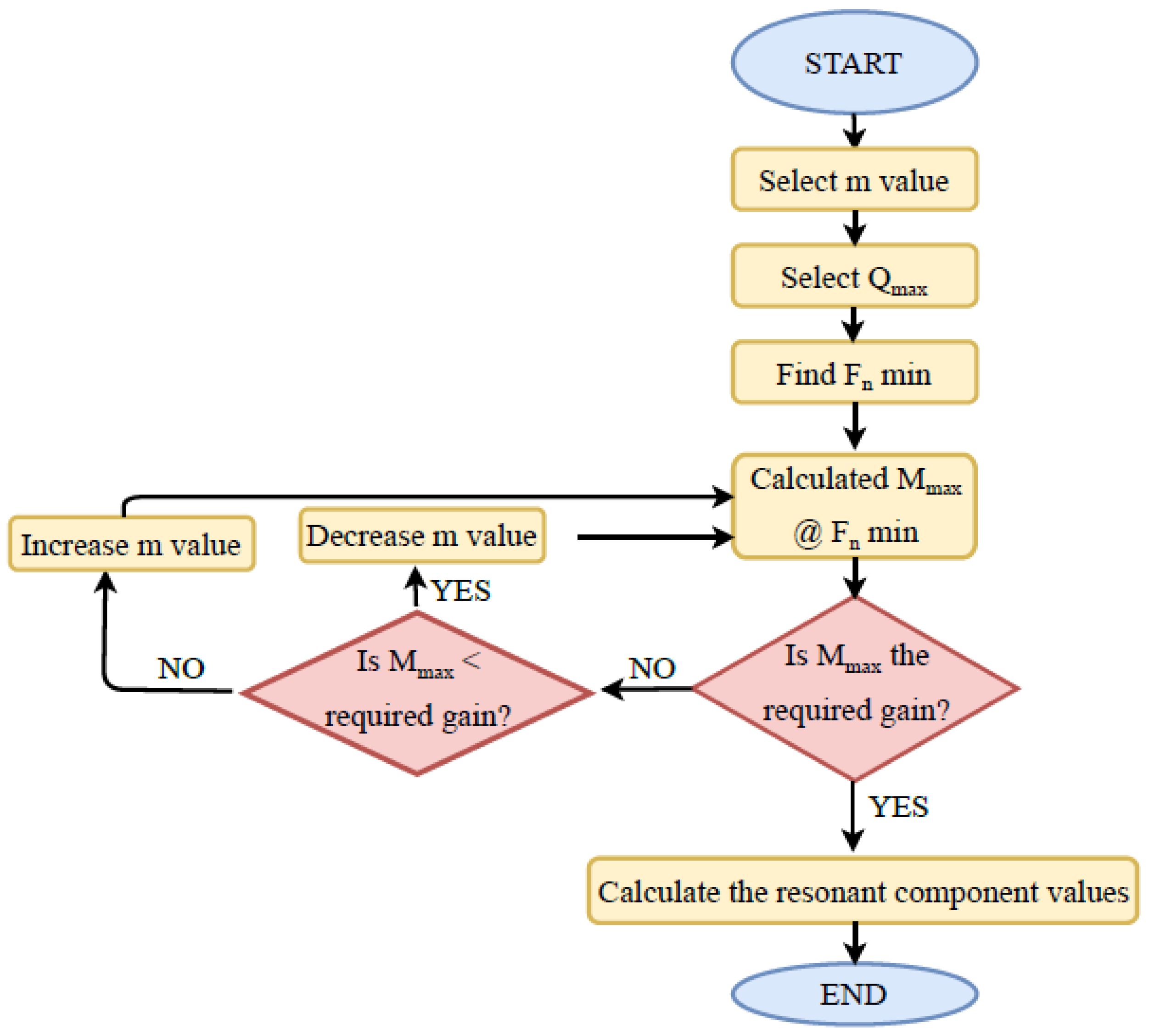
- The transformer inductance ratio (m) = (Lm + Lr)/Lr is another important parameter for the design. It is defined by the ratio of the primary magnetization inductance (Lm) and the equivalent leakage inductance (Lr). The transformer inductance ratio (m) is an important parameter that helps shape the gain curve. By selecting a smaller values of m, a higher voltage gain can be achieved with a narrow range of frequency modulation. Hence, lower values of m are more suitable for a wide input voltage range. On the other hand, choosing a small value of m means a very large Lr and a small value of Lm resulting in a very poor transformer coupling and thereby, reducing the efficiency due to a large circulating current [34]. A higher value of m increases the efficiency at the cost of a reduced voltage gain and a narrow range of frequency modulation. Therefore, the value of m is generally set between 3 and 7. An iterative method is normally employed to choose the optimal value of m based on input design parameters.
- The voltage gain after the integration of the transformer leakage differs from the voltage gain derived in Equation (3) by a multiple of Mv. This is the fixed gain at resonant frequency and it is given by:
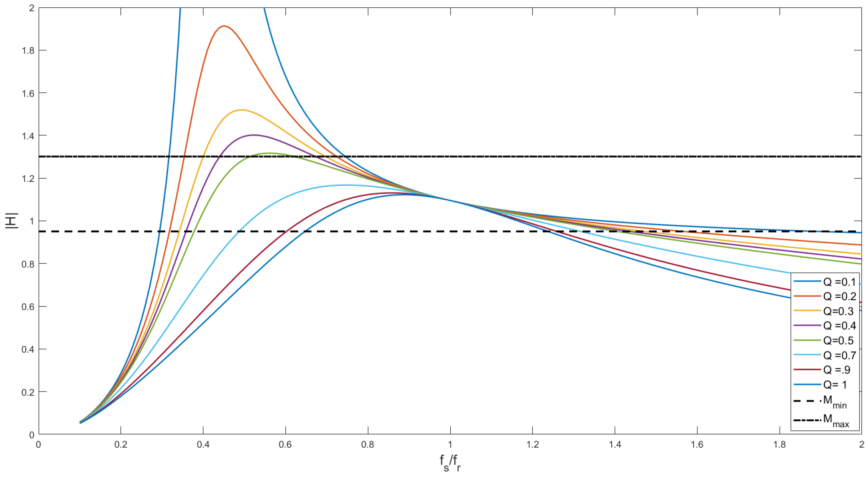
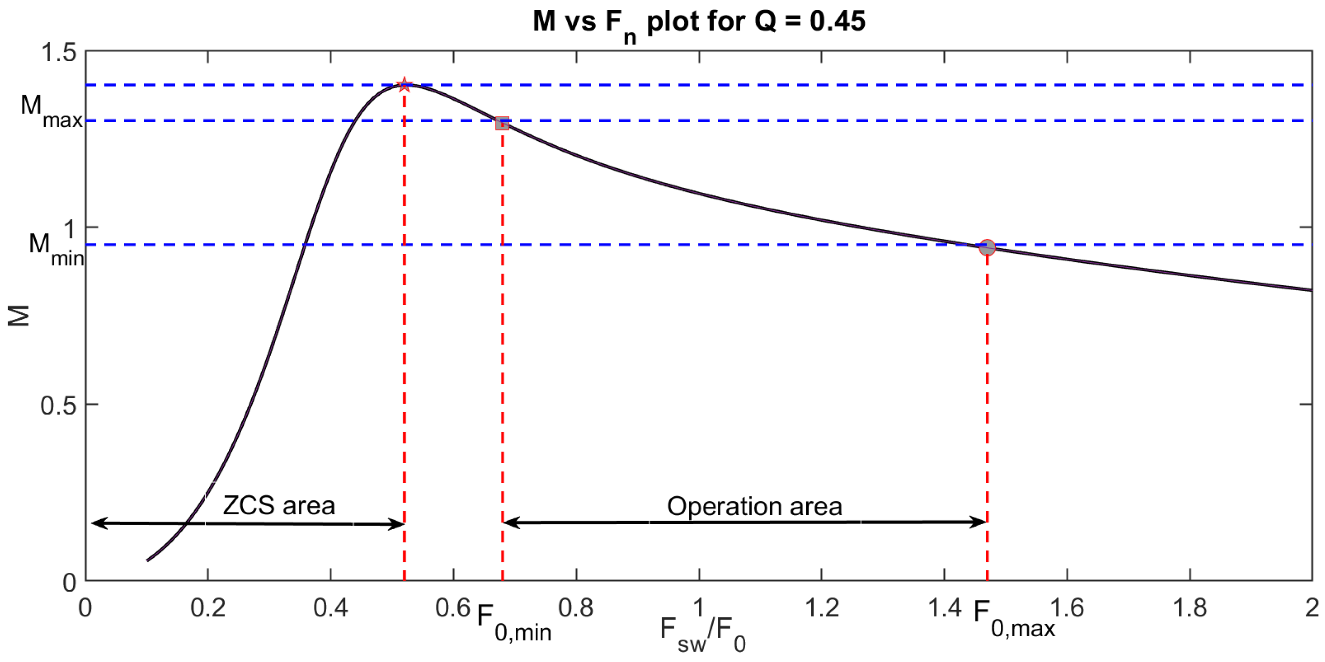
- The final step is to obtain the converter transfer function to attain the gain curve of the system. The time-domain analysis of an LLC converter is a very cumbersome process as the presence of nonlinear reactive elements in the converter and hence the resulting transfer function is typically nonlinear. To simplify the design procedure, first harmonic approximation (FHA) method is often employed. In this methodology, only the first harmonic signals are thought to contribute to power transfer. As a result, all current and voltage waveforms are presumed to be sinusoidal in nature. The FHA also helps determining the necessary constraints for the primary bridge to achieve ZVS. The transfer function ), also known as the voltage-gain function (i.e., ratio of output to input voltage) is shown in Equation (5).The real part of Equation (5) can be represented as:Plotting the gain vs. the normalized switching frequency with respect to the variable Q values gives an idea of which value of Qmax would satisfy the gain requirement. From Figure 9 it is evident that for m = 6 a Qmax = 0.45 would suffice.The gain curve is plotted again with the selected value of Qmax = 0.45 and m = 6 and shown in Figure 10. From the intersection of the maximum and minimum gain values, the frequency limit of inductive ZVS operation can be determined. The switching frequency must never go below the frequency where the peak occurs (as the converter enters a capacitive mode and it is not recommended).
- Finally the resonant tank parameters can be calculated from the following equations:
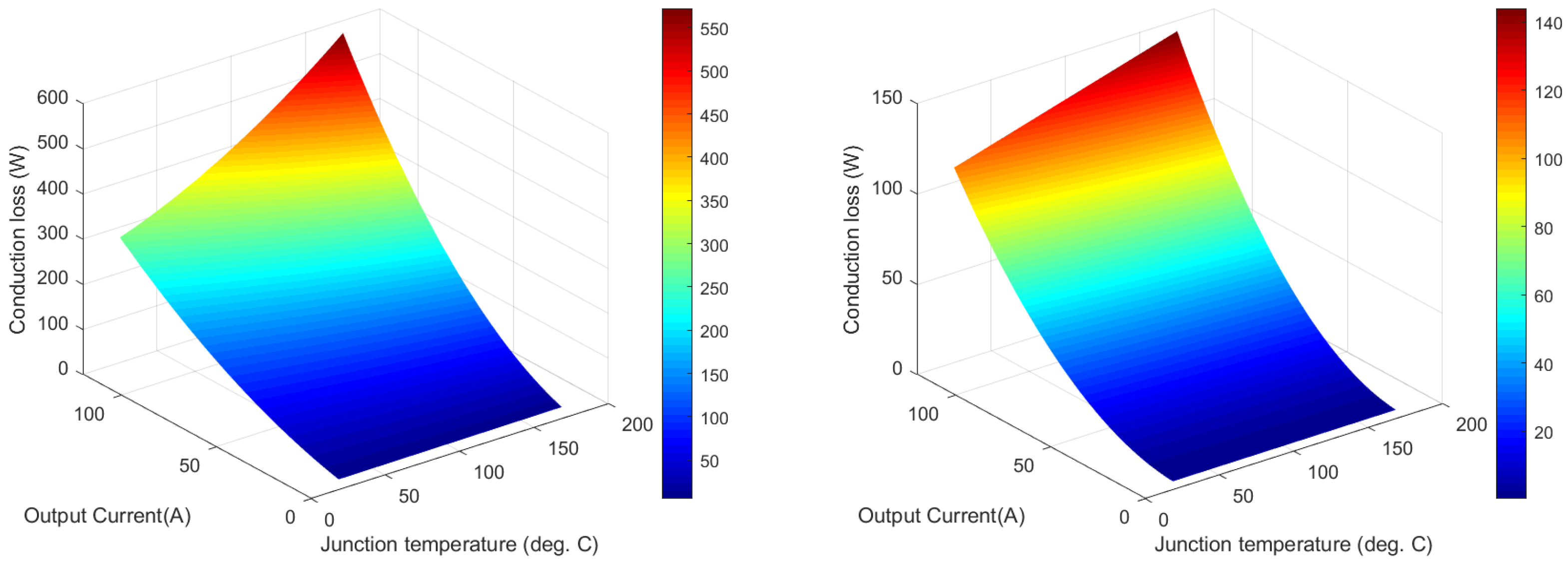
3.2. Secondary Stage Design
4. Control System
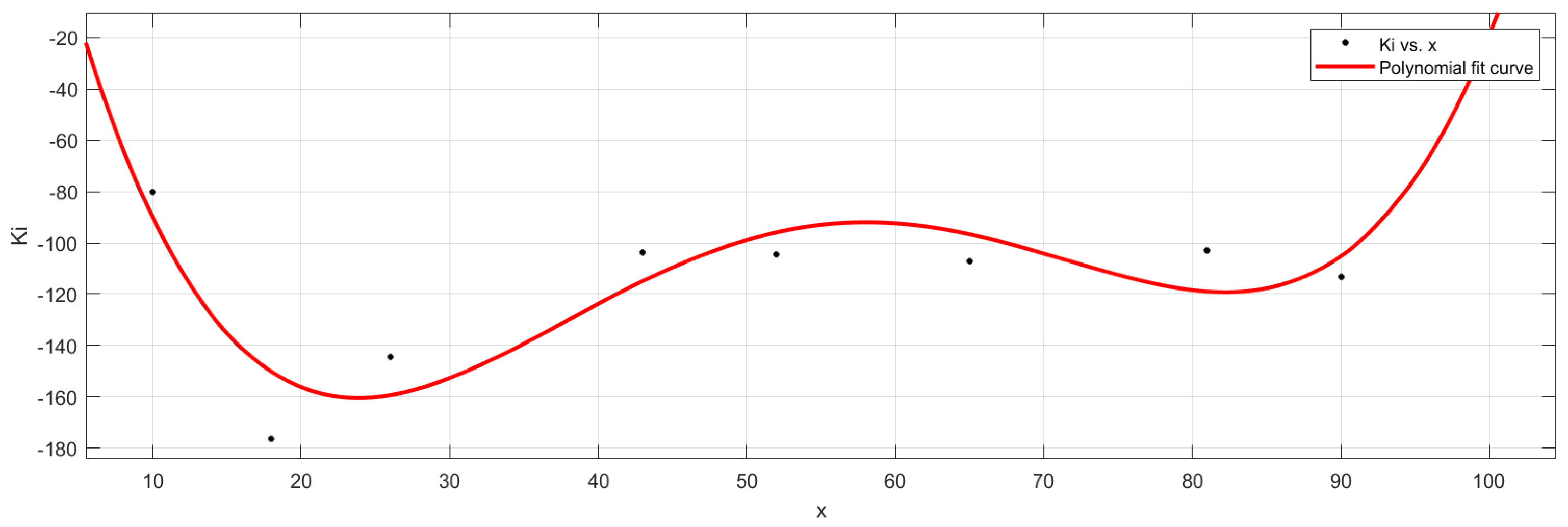
4.1. Gain Parameter Look–Up Table
4.2. Control Strategy
- In case of OC, the load current is limited and it is checked if the fault is cleared. Otherwise, the state is changed to SC1 or SCM based on the number of switches affected.
- In case of SCM or OCKM, the converter is unusable and the auxiliary battery must be engaged.
- In case of SC1, the converter enters the HB reconfiguration mode and decides which switches must be used to achieve HB operation based on the logic Table 2. Similar logic can be derived for the OCK1 state.
- The transition from FB mode to HB mode is accompanied with an SS sequence, in order to reduce the output voltage overshoot caused by the sudden inductive current step.
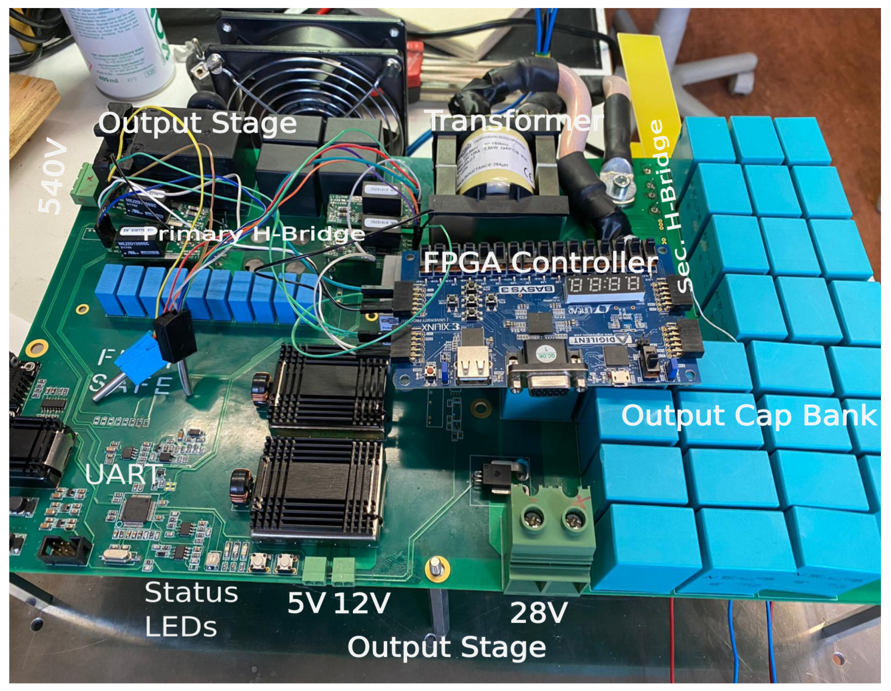
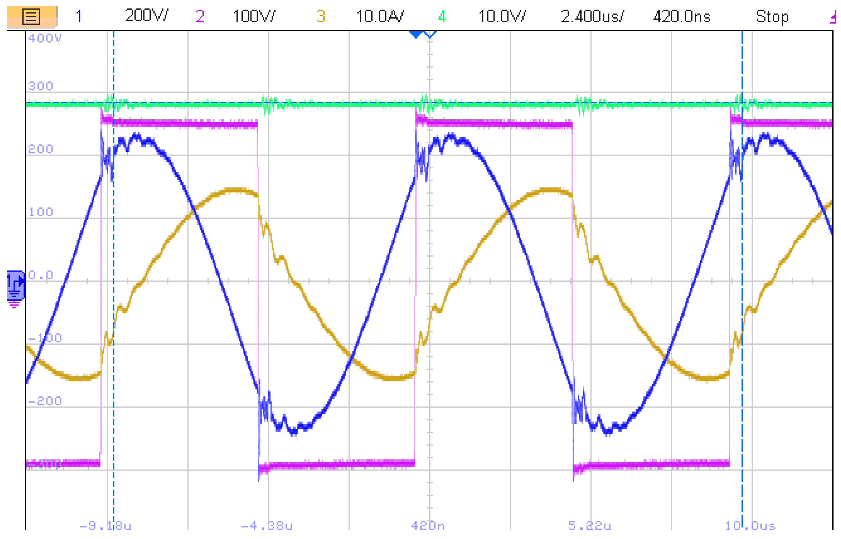
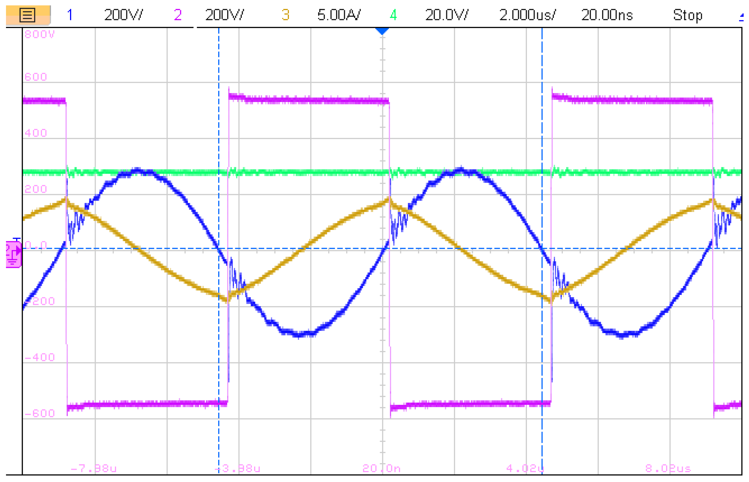
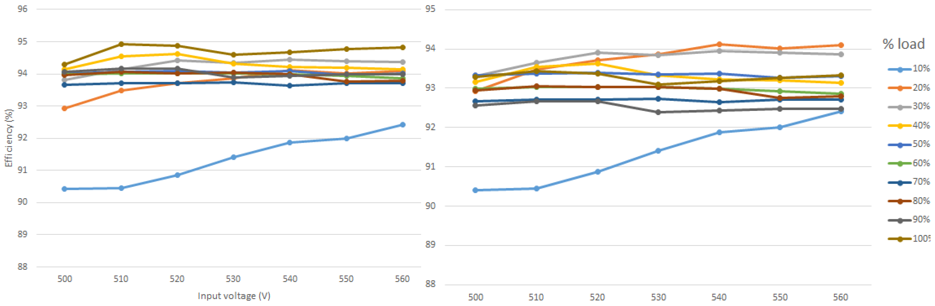
5. Experimental Results and Discussion
6. Conclusions
Author Contributions
Funding
Institutional Review Board Statement
Informed Consent Statement
Data Availability Statement
Acknowledgments
Conflicts of Interest
References
- Rosero, J.A.; Ortega, J.A.; Aldabas, E.; Romeral, L. Moving towards a more electric aircraft. IEEE Trans. Aerosp. Electron. Mag. 2007, 22, 3–9. [Google Scholar] [CrossRef] [Green Version]
- Revol, B.; Azzopardi, S.; Youssef, T.; Teu, J.S.N.; Gautier, C.; Khazaka, R.; Roggia, S. Overview and new trends in technology bricks for reliability enhancement in future wide band gap power converters for More Electrical Aircraft (MEA) and More Electrical Propulsion (MEP) systems. In Proceedings of the IECON 2019—45th Annual Conference of the IEEE Industrial Electronics Society, Lisbon, Portugal, 14–17 October 2019; pp. 7128–7134. [Google Scholar]
- Nawawi, A.; Tong, C.F.; Liu, Y.; Sakanova, A.; Yin, S.; Liu, Y.; Men, K.; See, K.Y.; Tseng, K.J.; Simanjorang, R.; et al. Design of high power density converter for aircraft applications. In Proceedings of the 2015 International Conference on Electrical Systems for Aircraft, Railway, Ship Propulsion and Road Vehicles (ESARS), Aachen, Germany, 3–5 March 2015; pp. 1–6. [Google Scholar]
- Swaminathan, N.; Cao, Y. An Overview of High-Conversion High-Voltage DC–DC Converters for Electrified Aviation Power Distribution System. IEEE Trans. Transp. Electrif. 2020, 6, 1740–1754. [Google Scholar] [CrossRef]
- Clements, R.; Jones, R.W. DC-DC convertor design for the 270 volts DC ‘More Electric Aircraft’. In Proceedings of the 2018 13th IEEE Conference on Industrial Electronics and Applications (ICIEA), Wuhan, China, 31 May–2 June 2018; pp. 1847–1852. [Google Scholar]
- Mastromauro, R.A.; Pugliese, S.; Stasi, S. An advanced active rectifier based on the single–star bridge cells modular multilevel cascade converter for more–electric–aircrafts applications. In Proceedings of the 2015 International Conference on Electrical Systems for Aircraft, Railway, Ship Propulsion and Road Vehicles (ESARS), Aachen, Germany, 3–5 March 2015; pp. 1–6. [Google Scholar]
- Hoenicke, P.; Ghosh, D.; Muhandes, A.; Bhattacharya, S.; Bauer, C.; Kallo, J.; Willich, C. Power management control and delivery module for a hybrid electric aircraft using fuel cell and battery. Energy Convers. Manag. 2021, 244, 114445. [Google Scholar] [CrossRef]
- Shi, B.; Zhou, B.; Hu, D. A novel dual–output indirect matrix converter for more electric aircraft. In Proceedings of the IECON 2017–43rd Annual Conference of the IEEE Industrial Electronics Society, Beijing, China, 29 October–1 November 2017; pp. 4083–4087. [Google Scholar]
- Raghavendra, K.V.G.; Zeb, K.; Muthusamy, A.; Krishna, T.N.V.; Kumar, S.V.S.V.P.; Kim, D.-H.; Kim, M.-S.; Cho, H.-G.; Kim, H.-J. A Comprehensive Review of DC–DC Converter Topologies and Modulation Strategies with Recent Advances in Solar Photovoltaic Systems. Electronics 2020, 9, 31. [Google Scholar] [CrossRef] [Green Version]
- Krishna, T.N.V.; Sathishkumar, P.; Himasree, P.; Punnoose, D.; Raghavendra, K.V.G.; Himanshu; Naresh, B.; Rana, R.A.; Kim, H.-J. 4T Analog MOS Control–High Voltage High Frequency (HVHF) Plasma Switching Power Supply for Water Purification in Industrial Applications. Electronics 2018, 7, 245. [Google Scholar] [CrossRef] [Green Version]
- Pugliese, S.; Mastromauro, R.A.; Stasi, S. 270 V/28 V wide bandgap device–based DAB converter for more–electric–aircrafts: Feasibility and optimization. In Proceedings of the 2016 International Conference on Electrical Systems for Aircraft, Railway, Ship Propulsion and Road Vehicles amd International Transportation Electrification Conference (ESARS–ITEC), Toulouse, France, 2–4 November 2016; pp. 1–6. [Google Scholar]
- Buticchi, G.; Costa, L.; Liserre, M. Improving System Efficiency for the More Electric Aircraft. IEEE Ind. Electron. Mag. 2017, 11, 26–36. [Google Scholar] [CrossRef]
- Rahrovi, B.; Ehsani, M. A Review of the More Electric Aircraft Power Electronics. In Proceedings of the 2019 IEEE Texas Power and Energy Conference (TPEC), College Station, TX, USA, 7–8 February 2019; pp. 1–6. [Google Scholar] [CrossRef]
- Peng, G.O.H.; Zhang, Y.; Dasgupta, S.; Husband, M.; Di, W.; Changyun, W. Fault Tolerant More Electric Engine/Aircraft Architecture with Integrated Condition–Based Control. In Proceedings of the 2018 IEEE International Conference on Electrical Systems for Aircraft, Railway, Ship Propulsion and Road Vehicles and International Transportation Electrification Conference (ESARS–ITEC), Nottingham, UK, 7–9 November 2018; pp. 1–6. [Google Scholar]
- Weimer, J.A. Electrical power technology for the more electric aircraft. In Proceedings of the AIAA/IEEE Digital Avionics Systems Conference, Fort Worth, TX, USA, 25–28 October 1993; pp. 445–450. [Google Scholar]
- Zhang, W.; Xu, D.; Enjeti, P.N.; Li, H.; Hawke, J.T.; Krishnamoorthy, H.S. Survey on fault–tolerant techniques for power electronic converters. IEEE Trans. Power Electron. 2014, 29, 6319–6331. [Google Scholar] [CrossRef]
- Ni, K.; Liu, Y.; Mei, Z.; Wu, T.; Hu, Y.; Wen, H.; Wang, Y. Electrical and Electronic Technologies in More–Electric Aircraft: A Review. IEEE Access 2019, 7, 76145–76166. [Google Scholar] [CrossRef]
- Pazouki, E.; de Abreu-Garcia, J.A.; Sozer, Y. Fault tolerant control method for interleaved DC–DC converters under open and short circuit switch faults. In Proceedings of the 2017 IEEE Energy Conversion Congress and Exposition (ECCE), Cincinnati, OH, USA, 1–5 October 2017; pp. 1137–1142. [Google Scholar]
- Palma, L.; Enjeti, P.N. A modular fuel cell, modular DC–DC converter concept for high performance and enhanced reliability. IEEE Trans. Power Electron. 2009, 24, 1437–1443. [Google Scholar] [CrossRef]
- Lian, Y.; Adam, G.; Holliday, D.; Finney, S. Modular input–parallel output-series DC/DC converter control with fault detection and redundancy. IET Gener. Transmiss. Distrib. 2016, 10, 1361–1369. [Google Scholar] [CrossRef] [Green Version]
- Haghnazari, S.; Vahedi, H.; Zolghadri, M.R. Fault tolerant operation strategy design for modular multilevel converters. In Proceedings of the IECON 2016–42nd Annual Conference of the IEEE Industrial Electronics Society, Florence, Italy, 23–26 October 2016; pp. 2172–2176. [Google Scholar]
- Deng, F.; Lü, Y.; Liu, C.; Heng, Q.; Yu, Q.; Zhao, J. Overview on submodule topologies, modeling, modulation, control schemes, fault diagnosis, and tolerant control strategies of modular multilevel converters. Chin. J. Electr. Eng. 2020, 6, 1–21. [Google Scholar] [CrossRef]
- Chen, G.; Chen, L.; Deng, Y.; Wang, K.; Qing, X. Topology-Reconfigurable Fault-Tolerant LLC Converter with High Reliability and Low Cost for More Electric Aircraft. IEEE Trans. Power Electron. 2019, 34, 2479–2493. [Google Scholar] [CrossRef]
- Zhao, N.; Liu, J.; Shi, Y.; Yang, J.; Zhang, J.; You, X. Mode Analysis and Fault–Tolerant Method of Open-Circuit Fault for a Dual Active-Bridge DC–DC Converter. IEEE Trans. Ind. Electron. 2020, 67, 6916–6926. [Google Scholar] [CrossRef]
- Huang, J.; Chen, G.; Shi, H. A Cost-Reliability Trade-Off Fault-Tolerant Series-Resonant Converter Combining Redundancy and Reconstruction. IEEE Trans. Power Electron. 2021, 36, 11543–11554. [Google Scholar] [CrossRef]
- Soon, J.L.; Lu, D.D. Design of Fuse–MOSFET Pair for Fault-Tolerant DC/DC Converters. IEEE Trans. Power Electron. 2016, 31, 6069–6074. [Google Scholar] [CrossRef]
- Costa, L.; Buticchi, G.; Liserre, M. A Fault-Tolerant Series-Resonant DC–DC Converter. IEEE Trans. Power Electron. 2017, 32, 900–905. [Google Scholar] [CrossRef] [Green Version]
- Bhattacharya, S.; Willich, C.; Hoenicke, P.; Kallo, J. A Novel Re-configurable LLC Converter for Electric Aircraft. In Proceedings of the 2021 IEEE 12th Energy Conversion Congress and Exposition-Asia (ECCE-Asia), Singapore, 24–27 May 2021; pp. 32–37. [Google Scholar] [CrossRef]
- Santini, T.; Sebastien, M.; Florent, M.; Phung, L.; Allard, B. Gate oxide reliability assessment of a SiC MOSFET for high temperature aeronautic applications. In Proceedings of the 2013 IEEE ECCE Asia Downunder—5th IEEE Annual International Energy Conversion Congress and Exhibition, Melbourne, VIC, Australia, 3–6 June 2013; pp. 385–391. [Google Scholar]
- Friedrichs, P.; Rupp, R. Silicon carbide power devices—Current developments and potential applications. In Proceedings of the 2005 European Conference on Power Electronics and Applications, Dresden, Germany, 11–14 September 2005. [Google Scholar]
- Musavi, F.; Craciun, M.; Gautam, D.S.; Eberle, W. Control Strategies for Wide Output Voltage Range LLC Resonant DC–DC Converters in Battery Chargers. IEEE Trans. Veh. Technol. 2014, 63, 1117–1125. [Google Scholar] [CrossRef]
- Miftakhutdinov, R.; Li, X.; Mukhopadhyay, R.; Wang, G. How to Protect SiC FETs from Short Circuit Faults–Overview. In Proceedings of the 2018 20th European Conference on Power Electronics and Applications (EPE’18 ECCE Europe), Riga, Latvia, 17–21 September 2018; pp. P.1–P.10. [Google Scholar]
- Texas Instruments Incorporated, Bi–Directional, Dual Active Bridge Reference Design for Level 3 Electric Vehicle Charging Stations, (Application Node: TIDUES0B–JUNE 2019–REVISED OCTOBER 2021). Available online: https://www.ti.com/tool/TIDA--010054 (accessed on 1 February 2021).
- Infineon Technologies Asia Pacific, Design Guide for LLC Converter with ICE2HS01G (Application Note, V1.0, July 2011). Available online: https://www.infineon.com/ (accessed on 1 February 2021).
- Texas Instruments Incorporated, Designing an LLC Resonant Half–Bridge Power Converter. Available online: https://www.ti.com/seclit/ml/slup263/slup263.pdf (accessed on 20 April 2022).
- Zeb, K.; Busarello, T.D.C.; Ul Islam, S.; Uddin, W.; Raghavendra, K.V.G.; Khan, M.A.; Kim, H.-J. Design of Super Twisting Sliding Mode Controller for a Three–Phase Grid–connected Photovoltaic System under Normal and Abnormal Conditions. Energies 2020, 13, 3773. [Google Scholar] [CrossRef]
- GeneSiC Semiconductor Inc. GC2X15MPS12–247 1200V 30A SiC Schottky MPS Diode (Datasheet, Revised July 2021). Available online: https://www.genesicsemi.com/ja/sic-schottky-mps/GC2X15MPS12-247/GC2X15MPS12-247.pdf (accessed on 20 April 2022).
- Wolfspeed Inc. C3M0015065K Silicon Carbide Power MOSFET C3M MOSFET Technology (Datasheet. Rev. 4.02.2021). Available online: https://assets.wolfspeed.com/uploads/2020/12/C3M0015065K.pdf (accessed on 20 April 2022).
- Gopiyani, A.; Patel, V. A closed–loop control of high power LLC Resonant Converter for DC–DC applications. In Proceedings of the 2011 Nirma University International Conference on Engineering, Gujarat, India, 8–10 December 2011; pp. 1–6. [Google Scholar] [CrossRef]
- Texas Instruments Inc. CSD18532KCS 60-V N–Channel NexFET Power MOSFET (Datasheet), August 2012–Revised July 2014. Available online: https://www.ti.com/product/CSD18532KCS (accessed on 20 April 2022).
- Texas Instruments Inc. LM74670–Q1 Zero IQ Smart Diode Rectifier Controller (74HC4051) Datasheet, October 2015. Available online: https://www.ti.com/product/LM74670-Q1 (accessed on 20 April 2022).
- Wolfspeed Inc. CGD15SG00D2 Gate Driver for Cree’s 3rd Generation (C3MTM) SiC MOSFET, Datasheet (CPWR–AN21, Rev. B.). Available online: https://www.wolfspeed.com/cgd15sg00d2/ (accessed on 20 April 2022).
- Digilent Inc. Basys 3 FPGA Board Reference Manual, Revised on 12.08.2014. Available online: https://digilent.com/ (accessed on 20 April 2022).


| Parameter | Value | Unit | |
|---|---|---|---|
| Input | Input voltage max (nom.) | 560 | V |
| Input voltage min (nom.) | 500 | V | |
| Abnormal Input voltage max (abnormal at 0.02 s) | 660 | V | |
| Abnormal Input voltage min (abnormal at 0.02 s) | 400 | V | |
| Preferred switching freq. | 50–200 | kHz | |
| Output | Output voltage (nom.) | 28 | V |
| Output voltage range | 22–29 | V | |
| Voltage ripple max | 1.5 | V | |
| Output power (nom.) | 2.0 | kW | |
| Output power (max) | 2.3 | kW | |
| Distortion factor (max) | 0.035 | ||
| Designed | Leakage inductance | 50 | H |
| Resonant | Magnetizing inductance | 275 | H |
| tank | Resonance capacitance | 47 | nF |
| Transformer turns ratio | 18:1:1 | ||
| Dead time | 350 | ns | |
| Resonance frequency | 98 | kHz | |
| Switching frequency max | 145 | kHz | |
| Switching frequency min | 67 | kHz |
| Q1 SC Fault | Q3 PWM | Q4 PWM | Q2 Open |
| Q2 SC Fault | Q3 PWM | Q4 PWM | Q1 Open |
| Q3 SC Fault | Q1 PWM | Q2 PWM | Q4 Open |
| Q4 SC Fault | Q1 PWM | Q2 PWM | Q3 Open |
Publisher’s Note: MDPI stays neutral with regard to jurisdictional claims in published maps and institutional affiliations. |
© 2022 by the authors. Licensee MDPI, Basel, Switzerland. This article is an open access article distributed under the terms and conditions of the Creative Commons Attribution (CC BY) license (https://creativecommons.org/licenses/by/4.0/).
Share and Cite
Bhattacharya, S.; Willich, C.; Kallo, J. Design and Demonstration of a 540 V/28 V SiC-Based Resonant DC–DC Converter for Auxiliary Power Supply in More Electric Aircraft. Electronics 2022, 11, 1382. https://doi.org/10.3390/electronics11091382
Bhattacharya S, Willich C, Kallo J. Design and Demonstration of a 540 V/28 V SiC-Based Resonant DC–DC Converter for Auxiliary Power Supply in More Electric Aircraft. Electronics. 2022; 11(9):1382. https://doi.org/10.3390/electronics11091382
Chicago/Turabian StyleBhattacharya, Sumantra, Caroline Willich, and Josef Kallo. 2022. "Design and Demonstration of a 540 V/28 V SiC-Based Resonant DC–DC Converter for Auxiliary Power Supply in More Electric Aircraft" Electronics 11, no. 9: 1382. https://doi.org/10.3390/electronics11091382
APA StyleBhattacharya, S., Willich, C., & Kallo, J. (2022). Design and Demonstration of a 540 V/28 V SiC-Based Resonant DC–DC Converter for Auxiliary Power Supply in More Electric Aircraft. Electronics, 11(9), 1382. https://doi.org/10.3390/electronics11091382