1. Introduction
This paper presents a 10-bit 5-MS/s successive approximation register (SAR) analog-to-digital converter (ADC) with a charge pump (CP) phase-locked loop (PLL) and a bootstrapped switch (referred to as PLL-SAR ADC) for a brushless direct current (BLDC) motor drive system. To meet system-on-chip and industrial requirements, we integrated the proposed SAR ADC and the control circuit of electric vehicles and implemented them by using the TSMC 0.25-μm high-voltage complementary metal oxide semiconductor (CMOS). There is a demand for reducing the power consumption and cost of electric vehicles through the use of a CP-PLL [
1], comparator, two bootstrapped switches, two monotonic capacitor arrays, SAR control logic, and digital error correction logic [
2]. Moreover, because the SAR ADC does not require a high-performance operational amplifier (OP Amp), its power consumption is remarkably low.
A BLDC motor drive is characterized by higher efficiency, lower maintenance, and higher cost. A new digital control concept for BLDC machines was introduced and experimentally verified. Because of the simplistic nature of this control concept, it can potentially be implemented in a low-cost, application-specific integrated circuit. Furthermore, this simplified control strategy does not require a state observer to regulate speed. A field programmable gain amplifier (PGA)–based novel digital pulse-width modulator (PWM) control scheme was developed to considerably reduce the system size and cost [
3]. A high-performance permanent-magnet synchronous motor driver IC featuring a scheme without position sensors and with current-sensing circuits was proposed. To produce current-sensing circuits, a 10-bit SAR ADC and various gain amplifiers were implemented in the fabricated IC [
4]. Sensing circuits and PGAs differ considerably in terms of the resolution of the SAR ADC. PGAs are used to amplify small voltages (~20 mV) that must be digitalized using 12-bit ADCs with up to 12.5 MS/s in motor control applications [
5]. A high-performance MCU-integrated PGA with a complete on-chip motor control solution was fabricated with a 65-nm CMOS. The switching noise was mitigated through the provision of an on-chip programmable R-bank, which can achieve the necessary noise filtering, along with on-board capacitors [
6]. That is, a completed on-chip motor control system can be implemented in the CMOS process.
The low-power low-noise integer-N divider-less technique can be employed to produce a digital PLL with high resolutions. A CP and a pulse-generation circuit are introduced to form the time-domain integral variable-gain amplifier to increase the resolution. A small-area SAR ADC is used to transform voltage signals into digital signals, thus avoiding the need for an analog filter, which occupies a large area. Compared with the conventional analog phase detector, the SAR ADC phase detector is compact and consumes less power [
1]. In general, the resolution of a SAR ADC with a PLL is restricted to 8 or 10 bits. An 8-bit SAR ADC was designed for transceivers for use in space communication. A CP-PLL was used to generate the reference clock signal of this SAR ADC, and its effective number of bits (ENOB) and signal-to-noise-and-distortion ratio (SNDR) were 7.7 bits and 48.15 dB, respectively. The main advantages of the SAR ADC are low power consumption, high speed, and high linearity because of its integer-based digital-to-analog converter (DAC) architecture [
7]. Furthermore, a 10-bit SAR ADC and PLL were employed with the TSMC 0.18-μm CMOS process for the optical sensors used in the depth cameras embedded in virtual reality and augmented reality applications. Using the Vcm-based switching method significantly reduced the switching power of the DAC, and the resulting SAR ADC with the PLL design used fewer capacitors in the DAC array [
8]. Moreover, a low-power reference-sampling digital PLL (RS-DPLL) equipped with a reference-sampling phase detector that used the bottom-plate sampling technique was proposed. The sampled voltage error was digitized using a gated amplifier incorporated with a compact 8-bit SAR ADC, resulting in a high resolution. The RS-DPLL, which was implemented using 28-nm CMOS technology, achieved a jitter of 355-fs rms and power consumption of only 1.1 mW [
9]. Combining SAR ADC with PLL is a popular solution in many industrial applications. Moreover, this design is suitable for the BLDC motor drive.
An efficient capacitor-switching procedure was presented for a 10-bit 50-MS/s SAR ADC [
10]. This switching procedure reduced both switching energy and total capacitance. Compared with the conventional switching procedure, this procedure had approximately 81% and 50% lower average switching energy and total capacitance, respectively. Moreover, the biased comparator reduced the dynamic offset induced by input common-mode voltage variation. However, this implementation was affected by process variations, and the coupling effect was not completely eliminated. To overcome this limitation, a dummy switch was used to improve the sample-and-hold accuracy. The dummy compensation mechanism removed the effect of clock feedthrough contributed by the observed voltage error to extremely low levels. The CMOS analog bootstrapped switch was found to be suitable for use in a high-precision sample-and-hold circuit [
11]. Subsequently, an SAR ADC equipped with a DAC consisting of grouped capacitors was implemented to reduce the bottom-plate parasitic capacitance threshold for the achievement of high speed and high power efficiency. The dual-path bootstrapped switch improved the sampling spurious-free dynamic range (SFDR) by more than 5 dB by isolating the critical signal from the N-well capacitance [
12].
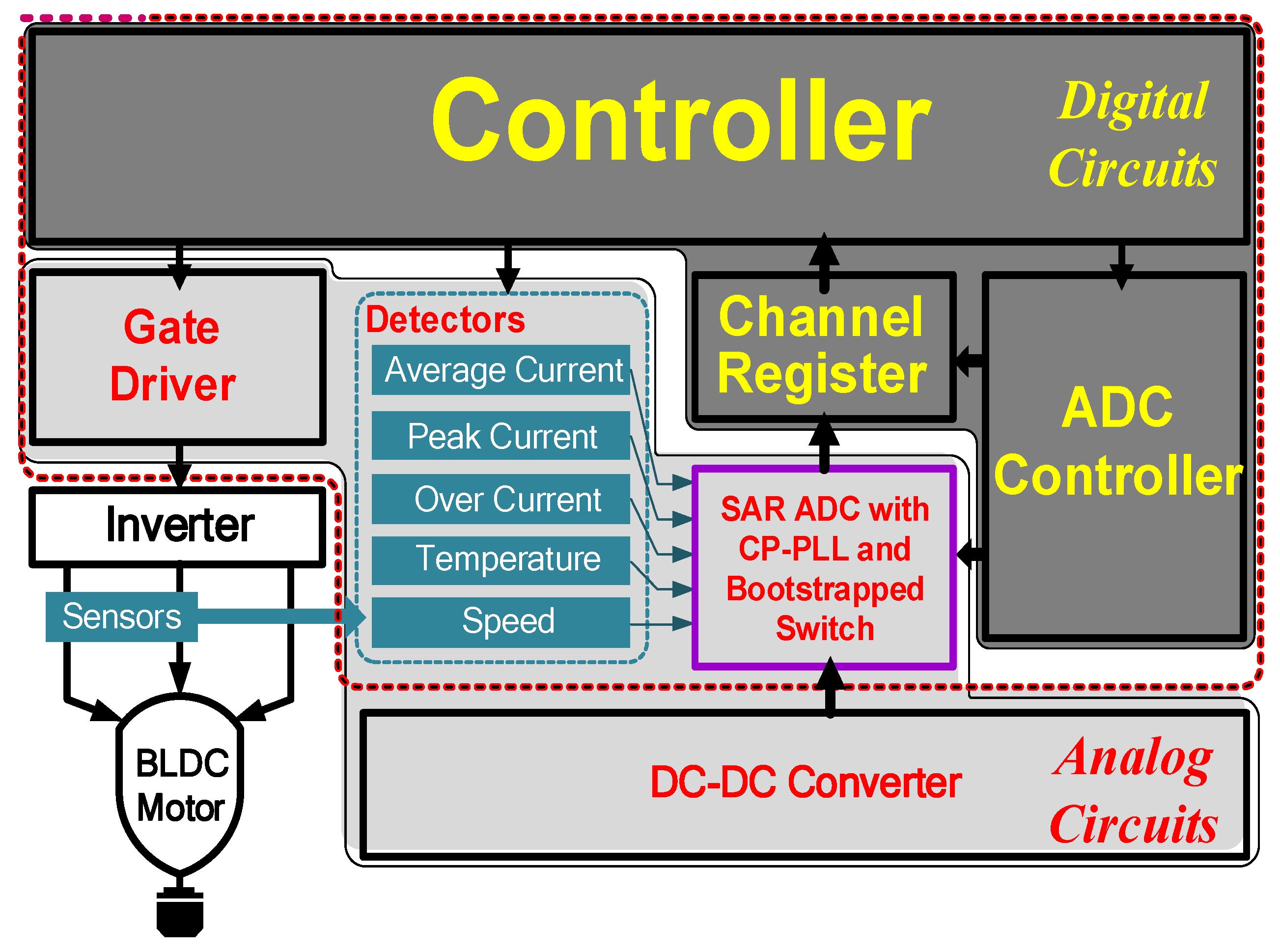
Figure 1 presents a system block diagram of an electric vehicle with a BLDC motor drive, which is composed of a digital controller, a channel register, an ADC controller, a gate driver, various detectors, a SAR ADC with a CP–PLL and bootstrapped switch, a direct current–direct current (DC–DC) buck converter, an inverter, and a BLDC motor [
13]. The digital circuits include the digital controller, channel register, and ADC controller, and the analog circuits include the gate driver, detectors, SAR ADC with a CP-PLL and bootstrapped switch, and DC–DC buck converter. Notably, multichannel detectors were used to detect and monitor useful parameters, including average current, peak current, overcurrent, temperature, and speed. After the sensing data are digitalized using the proposed SAR ADC, a digital control code is fed into the ADC controller to generate an appropriate PWM signal for controlling the gate driver and smoothly driving the BLDC motor. In brief, the designed SAR ADC is a key component in BLDC motor drive. The proposed PLL-SAR ADC performs with low power consumption, high sampling rate, and high linearity. It meets the requirements of SAR ADC in BLDC motor drive because the PWM register contains an 8-bit channel with clock frequencies of 0.25–8.0 MHz. An N-type buried layer is used to withstand high voltages through sharing of the bodies of all p-type metal oxide semiconductor field-effect transistors (PMOSFETs or PMOSs) in the TSMC 0.25-μm CMOS high-voltage process. We attempted to avoid shorting the source and body in the PMOSFETs. Furthermore, a dummy switch and a dummy transistor are added to improve the performance of the sample-and-hold circuit. The proposed SAR ADC provides a correct clock signal without an external signal generator. The remainder of this paper is organized as follows.
Section 2 elucidates the circuit design of the proposed SAR ADC with a CP-PLL and modified bootstrapped switch.
Section 3 presents the simulated and measured results.
Section 4 presents our concluding remarks.
2. Circuit Design of the Proposed PLL-SAR ADC
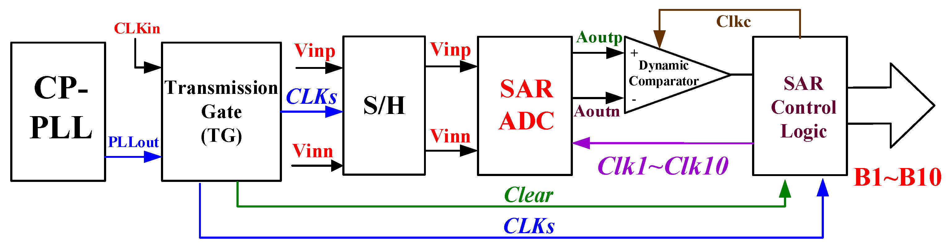
Figure 2 presents the system block diagram of the proposed PLL-SAR ADC with the modified bootstrapped switch. It was implemented with a monotonic capacitor-switching procedure to save power, CP-PLL to control the clock signal (CLKs), clear signal to reset the digital codes of the SAR control logic (Clear), and transmission gate (TG) to select the appropriate clock signal. Two clock signals, an external clock signal (CLKin) and an internal clock signal from the CP-PLL (
PLLout), are provided to guarantee that a correct
CLKs is obtained. After the design and verification of the proposed blocks, the PLL-SAR ADC system was fabricated with the TSMC 0.25-μm 1P3M CMOS high-voltage process for industrial applications through integration of the control circuits into a single chip.
2.1. System Design of the SAR ADC
In the single-ended architecture, only one end of the capacitor is switched. Consequently, the power consumption and the chip area are smaller than those of the dual-ended architecture. The advantage of the dual-ended architecture is that it can suppress any interference noise. Thus, combining the single capacitor-switching procedure with the dual-ended architecture yields a continuous progressive ADC with low power dissipation and the suppression of switching noise.
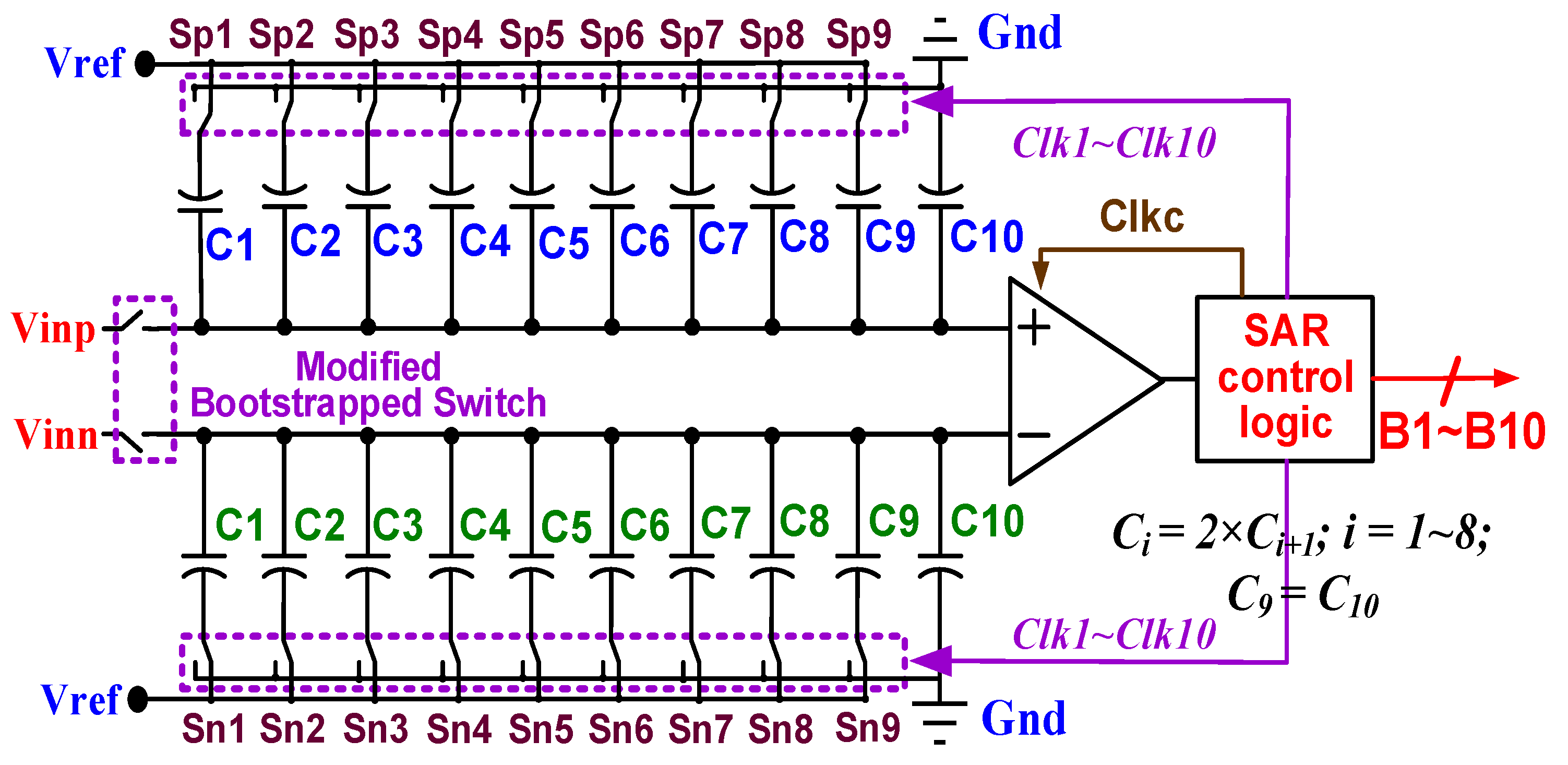
Figure 3 illustrates the dual-ended SAR ADC with the monotonic switching topology used herein. In the sample mode, the differential input signal passes through the sample-and-hold circuit (S/H) and samples the input signal against the upper plate of the capacitor array. The switches Sp1–Sp9 and Sn1–Sn9 are switched to the reference voltage
Vref, which is connected to the power supply
VDD. In the first cycle (
Clk1), the comparison begins with the use of the differential input voltages
Vinp and
Vinn, and all of the switches remain unchanged. If the positive input voltage
Vinp is higher than the negative input voltage
Vinn, then the first output bit B1 is set to 1. In the second cycle (
Clk2), the first weighted capacitor
C1 on the positive side is switched to the ground voltage (
Gnd = 0 V) through switching of the first positive switch Sp1. The other positive switches Sp2–Sp9 and negative switches Sn1–Sn9 remain unchanged. If
Vinp is higher than
Vinn, then the second output bit B2 is set to a high voltage (
Vref) and the second weighted capacitor
C2 on the positive side is connected to
Gnd. If not, the second output bit B2 is set to a low voltage (
Gnd), the second capacitor
C2 on the negative side is switched to
Gnd, and the remaining capacitors remain connected to
Vref. This switching procedure continues until the minimum output bit (B10) is obtained. The power consumption of this capacitance switching is effectively reduced because switching is only performed with one side of the capacitor. Two basic capacitors (
C11) at upside and downside and four switches (Sp10–Sp11 and Sn10–Sn11) are eliminated, leading to a significantly smaller chip area and significantly less switching noise compared with those of the conventional 10-bit SAR ADC [
10].
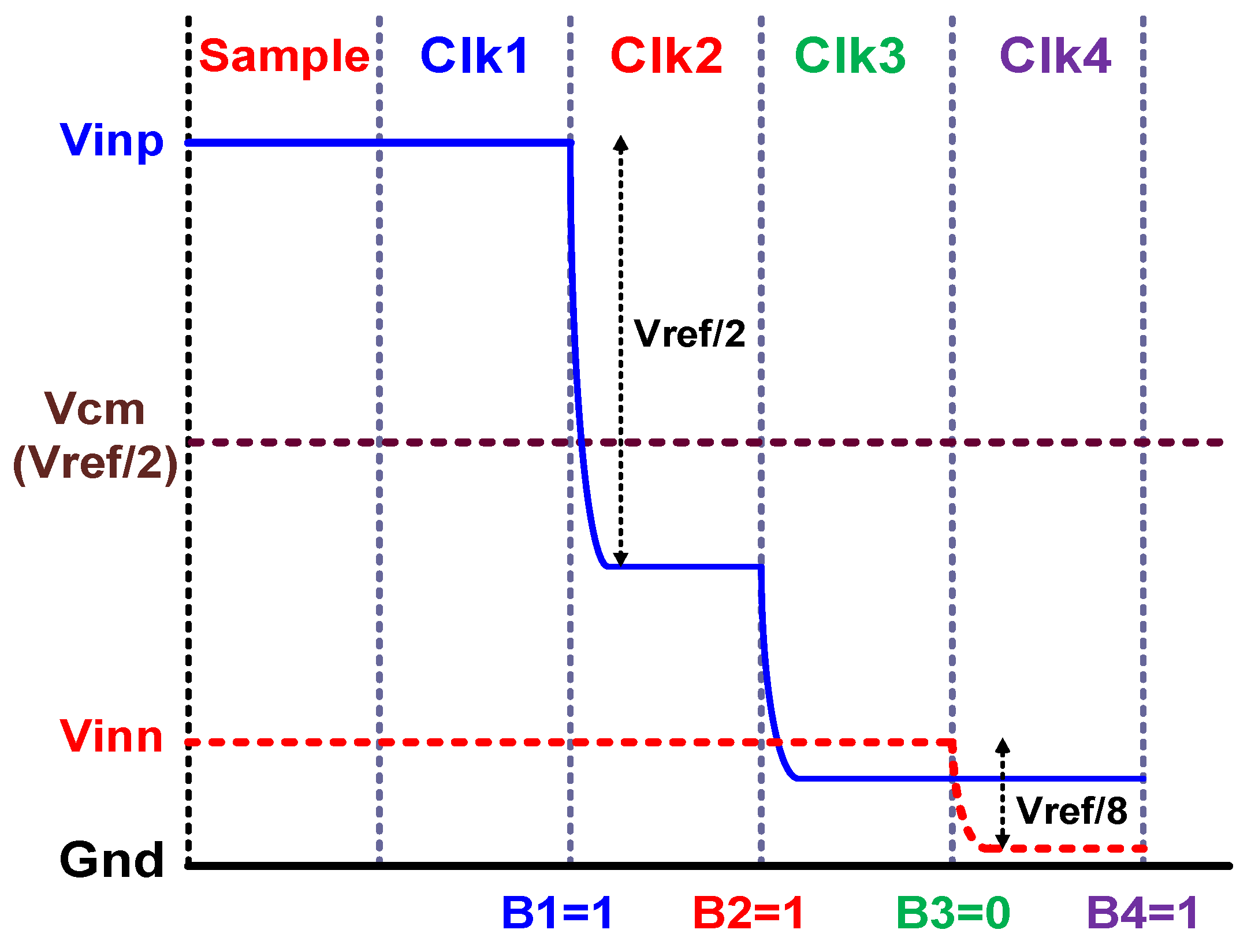
Figure 4 shows the adopted monotonic switching procedure, which does not require upward transition and performs sampling on the top plate. These features accelerate DAC settling. In addition, the first comparison can be performed without any capacitor switching in the first clock (
Clk1), as illustrated in
Figure 4. In
Clk2, the adopted switching sequence reduces
Vinp to (
Vinp-
Vref/2) and maintains the negative input voltage
Vinn. In
Clk3, the positive input voltage
Vinp is reduced to (
Vinp-
Vref/2-
Vref/4), and the negative input voltage
Vinn is unchanged. In
Clk4, the negative input voltage is reduced to (
Vinn-
Vref/8), and the positive input voltage
Vinp remains unchanged. The switching procedure continues until the ground voltage is reached. In contrast to the conventional switching procedure [
10], the proposed procedure only requires the downward transition to be switched in each comparison. The monotonic capacitor-switching procedure thus reduces power consumption and switching noise.
2.2. Modified Bootstrapped Switch with a Dummy Switch and Dummy Transistor
In the sample mode, a modified S/H is used to sample the differential input voltage, which is affected by the changing switch impedance. As the control signal (
PLLout) is fed into the switch from the CP-PLL, distortion occurs as a result of the changing switch impedance, which increases the signal noise and distortion and reduces the signal-to-noise ratio (SNR) and SNDR. To overcome this problem, a good switch with a small on-resistance must be identified.
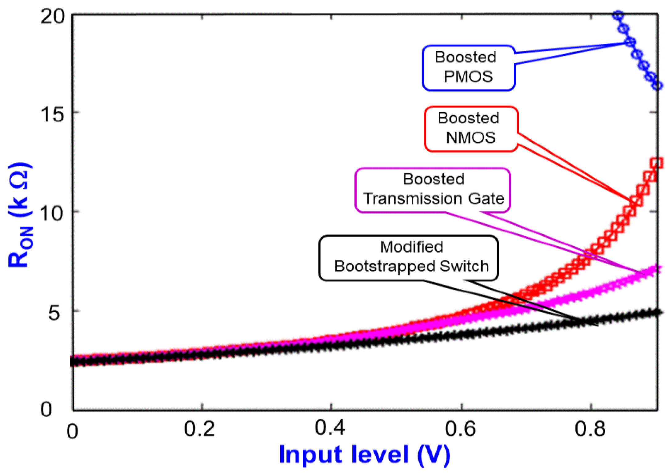
Figure 5 depicts the simulated on-resistance
Ron with respect to the input levels of various switches, including the boosted PMOS, boosted NMOS, boosted TG, and modified bootstrapped switch with a constant gate-to-source voltage (
Vgs). The modified bootstrapped switch operates with a small and linear conducting impedance.
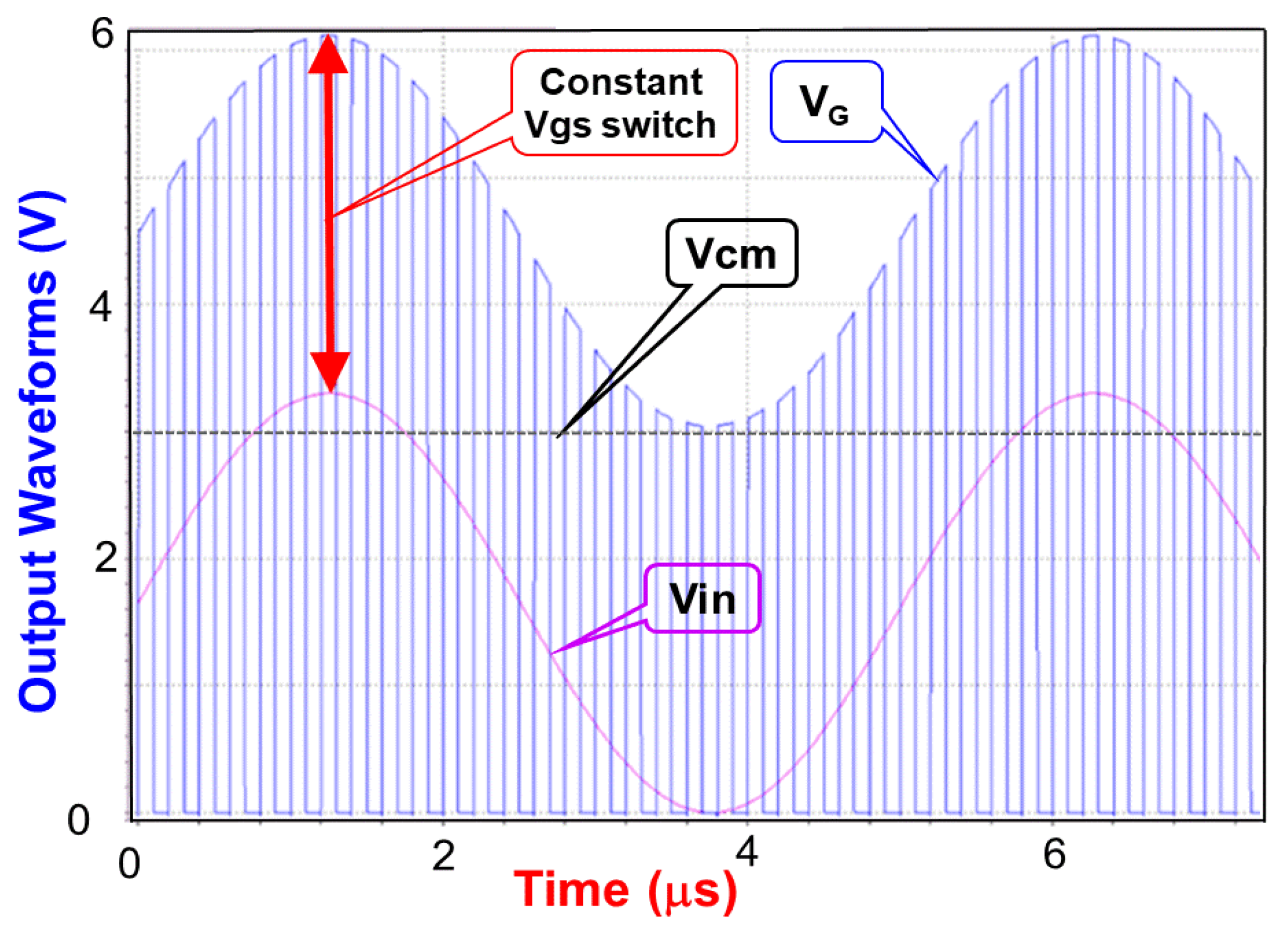
Figure 6 illustrates the simulated output waveforms of the modified bootstrapped switch. Notably, the
Vgs remains constant between the gate voltage
VG and the input signal
Vin.
Figure 7 depicts the modified sample-and-hold circuit with a constant
Vgs switch and a dummy switch. It is composed of a sampling capacitor Cs and a bootstrapped switch MH
9 to facilitate operation with low power dissipation and a wide bandwidth. The boosted driver causes periodic output switching between (
Vdda +
Vinp) and
Vinp by using the analog positive power supply
Vdda and the input voltage
Vinp. Two PMOSs, namely MH
3 and MH
5, are used to rectify the errors caused by the charge injection and clock feedthrough because these switches operate interactively. If
CLKs = 0, then the NMOSs MH
4, MH
7, and MH
11 are turned on simultaneously. The voltage
VG is set to 0 V after it has passed through MH
6 and MH
7. Next, the PMOS MH
3 is turned on due to the gate voltage
VG (0 V). The sampling capacitor C
S is rapidly charged to
Vdda. Meanwhile, MH
5 is turned off upon its connection to
Vdda through MH
1 and two NMOSs, namely MH
8 and MH
9, are turned off upon their connection to the gate voltage
VG (0 V). By contrast, if
CLKs = 1, then the gate voltage of MH
5 is set to the ground voltage (0 V) to activate MH
5. Subsequently, the gate voltage
VG is charged to
Vdda. The voltage difference between the power supply voltage (
Vdda) and ground voltage (
Vssa) is stored in the sampling capacitor C
S. When the positive input voltage
Vinp is fed to MH
8, the voltage
VG is charged upward to (
Vdda +
Vinp). Next, the gate-to-source voltage
Vgs8 of MH
8 is fixed to
Vdda regardless of the variation of the input voltage
Vinp. That is, the positive output voltage
Soutp is not adversely affected by the errors in MH
8 and MH
9, which are induced by charge injection and clock feedthrough. Notably, a dummy switch MH
10 is added to increase precision by reducing the coupling effect and on-resistance [
11].
As illustrated in
Figure 7, the positive output voltage
Soutp is achieved at the corresponding inputs of
Vinp and
Vinn after passage through MH
9 and MH
10, respectively. The corresponding inputs
Vinn and
Vinp are connected to MH
9 and MH
10, respectively, to obtain the negative output voltage
Soutn. A dummy switch MH
10 is added to reduce the clock feedthrough and eliminate voltage disturbance, which is induced by the parasitic capacitance
Cds at the S/H capacitor C
H [
2]. Furthermore, a dummy transistor MH
11, driven by
, is added to the circuit such that after MH
9 and MH
10 are turned off and MH
11 is turned on, the channel charge deposited on C
H is absorbed by the dummy transistor MH
11 to alleviate the error induced by charge injection and to improve the switch linearity [
14].
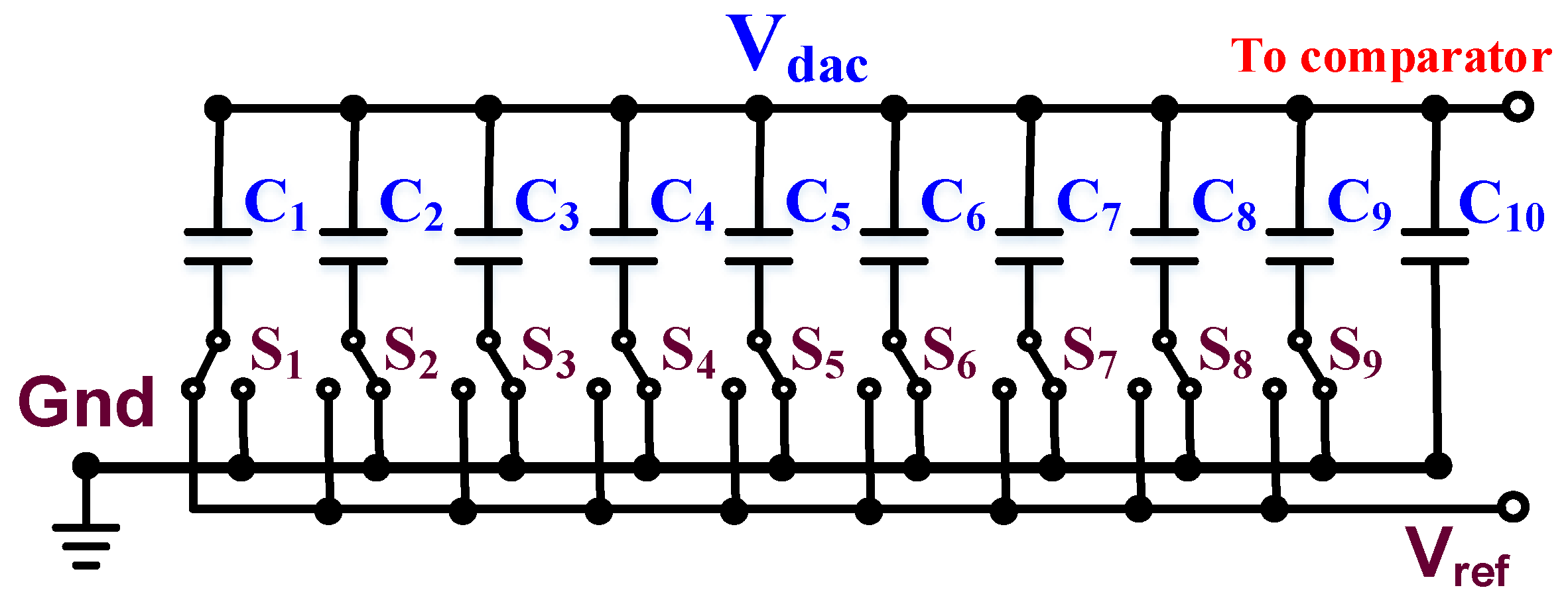
2.3. Binary-Weighted Capacitor Array DAC
The DAC is used to convert the digital codes at the output of the SAR logic into an analog signal. The analog signal is then compared with the input signal with a comparator. The DAC is generally composed of resistors or capacitor arrays. To reduce power consumption, a 10-bit binary-weighted capacitive DAC (CDAC) is considered herein, as illustrated in
Figure 8. This DAC is composed of 10 binary-weighted capacitors (
C1–
C10) and a set of switches (S
1–S
9). The capacitance relationship is
Ci = 2 ×
Ci+1 and
C9 =
C10, where
i = 1–8.
The maximum settling time of a DAC is usually determined by the charge and discharge procedure of the most significant bit (MSB) and by the conversion speed of the MSB with the maximum offset. Thus, the decoding error is greater than all of the noise sources, which reduces the SNR if the DAC is poorly designed. To realize a high-resolution DAC, these mismatches, which are induced by practical capacitors and parasitic capacitors, must be analyzed and eliminated. If the maximum capacitor
C1 is connected to
Vref with an error rate of ε and the remaining capacitors (
C2–
C10) are connected to the ground, the output voltage of the DAC with a mismatch capacitor can be expressed as follows:
Let us assume that the reference voltage
Vref is 3.3 V and the resolution is 10 bits; the ideal output voltage of the DAC
Vdac (
ideal) is thus 1.65 V, which is half of the reference voltage. The maximum error rate ε can be calculated as follows.
The DAC is extremely sensitive to switch ratio and capacitor mismatch, especially in case of the minimum capacitor
C0. The capacitor layout must be designed carefully to eliminate the mismatch effect [
15].
2.4. Modified Two-Stage Dynamic Comparator
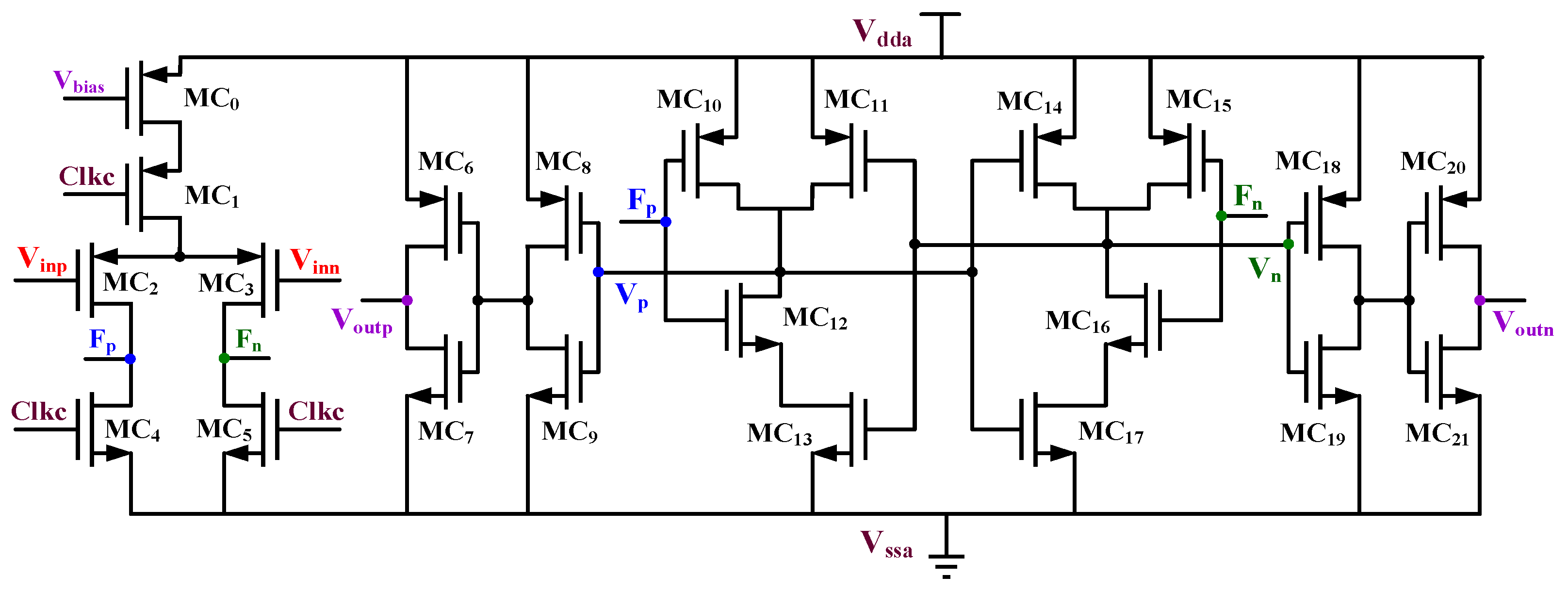
A dynamic latch-type comparator is used to rapidly latch the voltage difference between the two inputs Vinn and Vinp to the high level (1) or low level (0) through positive feedback. The dynamic latch comparator does not consume static power, unlike the open-loop amplifier. For a single capacitor, the comparator has a pull-down switching design. That is, the common-mode voltage at the comparator input is switched between Vref/2 and Vssa. This means that the dynamic comparator must be operated at a low voltage. To this end, a differential pair, which is established in the PMOSs, is a good choice.
Figure 9 illustrates a modified two-stage dynamic comparator [
16]. When the clock signal
Clkc is high, two n-type metal oxide semiconductor field-effect transistors (NMOSFETs or NMOSs) MC
4 and MC
5 are turned on. The dynamic comparator operates in the reset mode, and the two float voltages
Fp and
Fn are connected to the ground. Next, two PMOSFETs, MC
10 and MC
15, are turned on, and the power voltage
Vdda is directly connected to two internal voltages
VP and
Vn. When passing through two NOT gates, the two output voltages
Voutp and
Voutn are high. Notably, the NMOSFET MC
1 is turned off when
Clkc = 1 (high), as is the dynamic comparator. Therefore, it does not consume any static current. By contrast, when the clock signal
Clkc is low (0), MC
4 and MC
5 are turned off and MC
1 is turned on. The dynamic comparator operates in the comparison mode. The two float voltages
Fp and
Fn are then determined according to the two inputs
Vinp and
Vinn. If
Vinp >
Vinn, then
Fp <
Fn. When passing through two inverters, MC
10–MC
13 and MC
14–MC
17,
Vp >
Vn. Finally, the positive output voltage
Voutp is higher than the negative output voltage
Voutn. A higher input voltage
Vinp corresponds to a higher output voltage
Voutp. The modified two-stage dynamic comparator can prevent kickback noise and is insensitive to the input signal.
Taking the input-stage of the dynamic comparator as an example, the input offset voltage
Vos can be expressed as follows [
17]:
where Δ
VTH2,3 is the threshold voltage mismatch of the two input PMOSFETs MC
2 and MC
3. Δ
S2,3 is the mismatch in physical dimensions between MC
2 and MC
3. Δ
R is the resistor mismatch of the load resistance, which is contributed by the two NMOSFETs MC
4 and MC
5. As expressed in (5), the first term represents a static offset, which does not affect the performance of the ADC, whereas the second term is a dynamic offset, which is affected by variation in the common-mode voltage. The offset voltage
Vos can be reduced through a decrease in the overdrive voltage (
VGS −
VTH)
2,3 through MC
2 or MC
3. Thus, the gate of MC
0 is connected to
Vbias to reduce the offset error in the second term. Moreover, the two NMOSFETs, MC
12 and MC
16, are added not only to reduce the offset error but also to enhance the linearity of the modified dynamic comparator.
2.5. Modified SAR Control Logic
The continuous progressive controller is implemented with CMOS circuits. The designed functions of the SAR control logic include controlling the reset signal of the dynamic comparator, managing the switching action of the DAC, storing the comparison result of the comparator, and exporting the digital codes.
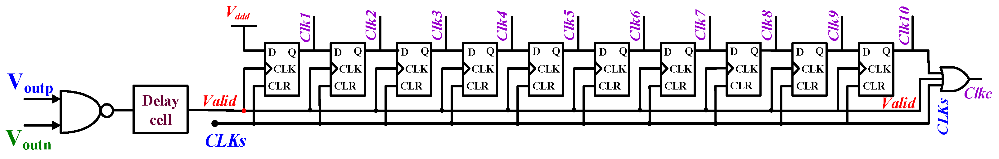
A modified asynchronous SAR control logic circuit is proposed to generate the necessary clock signals through the addition of a delay cell to guarantee that the output clock signals are asynchronous [
10].
Figure 10 shows a schematic of the modified asynchronous SAR control logic circuit with the digital power supply
Vddd, which is used not only to accept the two control signals
Valid and
CLKs but also to generate a comparison signal
Clkc and 10 asynchronous clock signals
Clk1–
Clk10. The signal
CLKs is fed through the TG to reset the control logic. The signal
Valid is generated from two output voltages of the modified dynamic comparator
Voutp and
Voutn. The clock signals
Clk1–Clk10 sample the digital output codes of the two-stage dynamic comparator and furnish them to the capacitor arrays to execute the monotonic switching procedure.
Table 1 summarizes the state table of the SAR control logic for controlling the DAC switches. As the dynamic comparator completes the comparison, the signal
Valid is sent to the asynchronous SAR control logic circuit to trigger the clock signals in order and maintain them at a high level (
Vddd). If the reset signal (
Clear) starts at
CLKs = 1 (high), the clock signals
Clk1–Clk10 are reduced to the low level (Gnd). A delay cell is added to the asynchronous control logic circuit to guarantee that the output level of the capacitor array remains stable. This means that the time delay of the delay cell must be longer than the settling time of the DAC capacitor array.
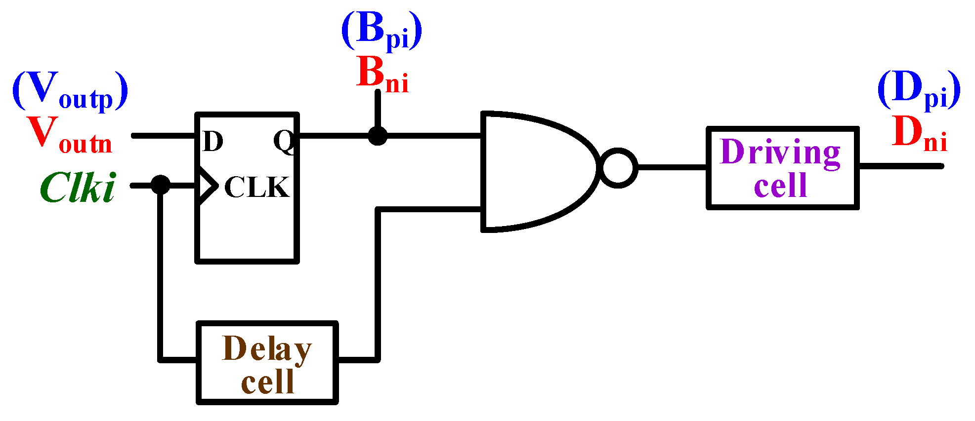
The designed DAC control circuits are divided into two categories: N-type and P-type. Each type operates with 10 DAC control circuits. That is, there are 20 DAC control circuits in the asynchronous SAR control logic circuit.
Figure 11 presents the modified DAC control circuit [
10], which includes
Voutn/
Voutp,
Clki,
Bni/
Bpi, and
Dni/
Dpi. The integer
i refers to an
i-bit control signal. The output voltages
Voutn and
Voutp are captured using the dynamic comparator circuit. The output clock signal
Clki of the asynchronous SAR control logic circuit is used to control the switching procedure of the DAC. Because
Clki is positive-edge triggered, the captured output voltage
Voutn/
Voutp is transferred to the output voltage of a D-type flip-flop (DFF)
Bni/
Bpi. After passage through the NAND gate, the output control signal
Dni/
Dpi for controlling the DAC capacitor array is obtained. For example, if
Voutp = 1 (high), then
Dpi = 0. The lower plate of the capacitor is connected to
Vssa from
Vref. If
Voutn = 0, then
Dni = 1 (high). That is, the lower plate of the capacitor operates without action. Notably, a driving cell is added to alleviate the switching error of the high binary-weighted DAC capacitor array.
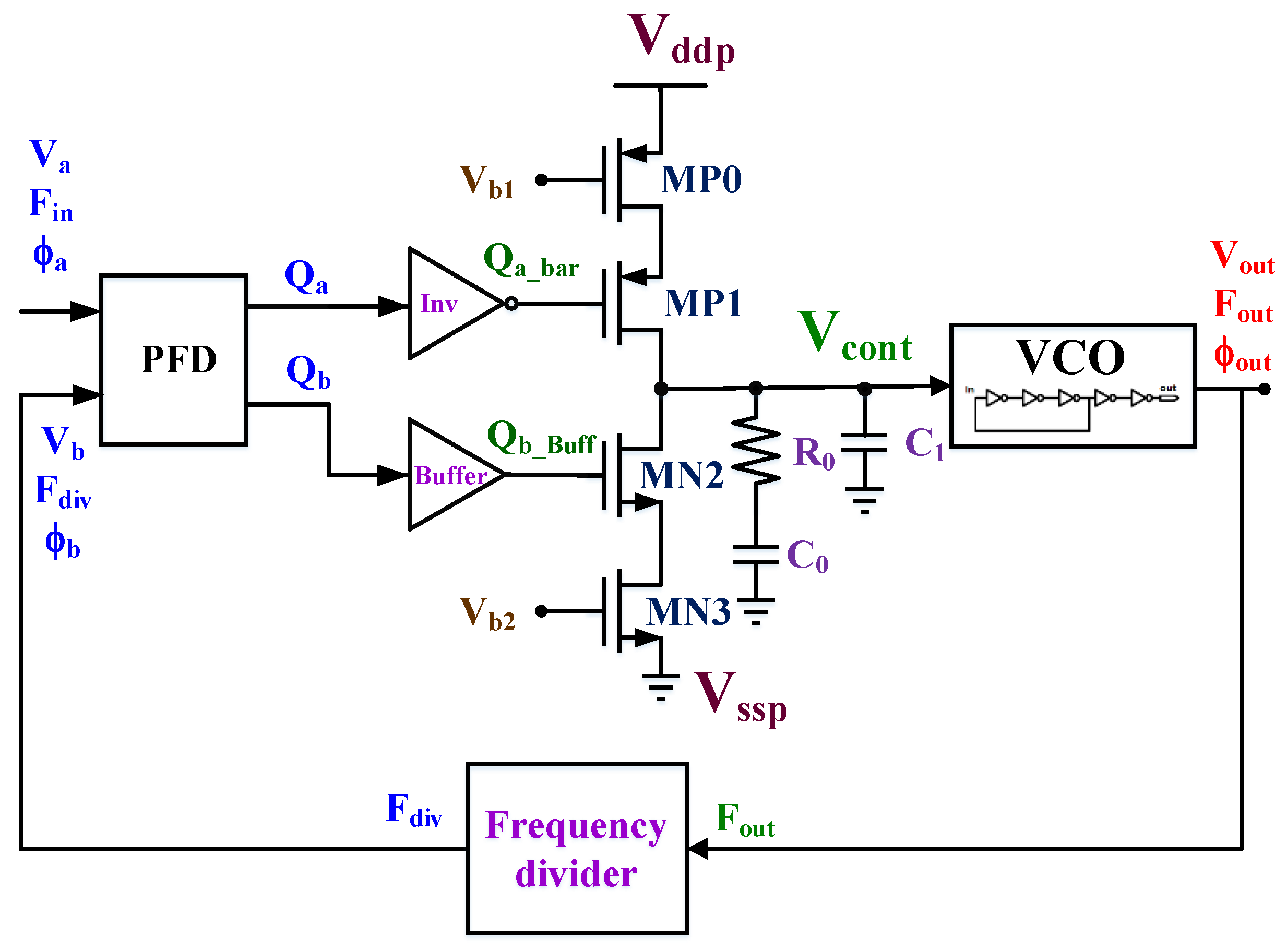
2.6. Fundamental PLL
A fundamental PLL was adopted to guarantee that the frequency (
F) and the phase (ϕ) of the input reference signal
Va and the feedback signal
Vb are the same.
Figure 12 depicts the adopted fundamental PLL, which includes a phase frequency detector (PFD), CP, loop filter, voltage-controlled oscillator (VCO), and frequency divider (FD) [
18,
19]. The operating principle of the fundamental PLL can be described as follows: the PFD detects the phase difference (Δϕ) between the input reference signal (
Va) and the feedback signal (
Vb) and transmits two output signals
Qa and
Qb to the CP for the subsequent stage. The inverse voltage
Qa_bar passing through the inverter and the buffer is used to control the PMOSFET MP
1, and the buffer voltage
Qb_Buff is used to control the NMOSFET MN
2. That is, two control signals
Qa_bar and
Qb_Buff are connected to the gates of MP
1 and MN
2, respectively, to charge or discharge the loop filter, which is composed of a resistor R
0 and two capacitors
C0 and
C1. A control voltage
Vcont is then generated to change the output frequency
Fout of the VCO. The output frequency
Fout passing through the FD is divided to generate a feedback frequency
Fdiv, which is close to the input reference frequency
Fin and reduces the phase difference (Δφ) between φ
a and φ
b. This procedure is repeated until Δφ = 0. The function of the fundamental PLL is to guarantee that the frequency and phase of V
a are identical to those of V
b. However, only a clock signal appears in the traditional SAR ADC. It requires an external clock generator and fails to guarantee the synchronous operation between
Va and
Vb.
VCO generates an output frequency Fout based on the control voltage Vcont. The ring oscillator is a popular oscillator, and it is implemented without passive components. This feature is suitable for fabrication in the CMOS process. In general, a ring oscillator is composed of an odd number of inverters. The delay time td is inherent in the inverter from the input to the output, and vice versa. When a ring oscillator is initiated, the oscillation frequency fosc is equal to 1/(2 × td). The greater the odd number of inverters, the lower the oscillation frequency.
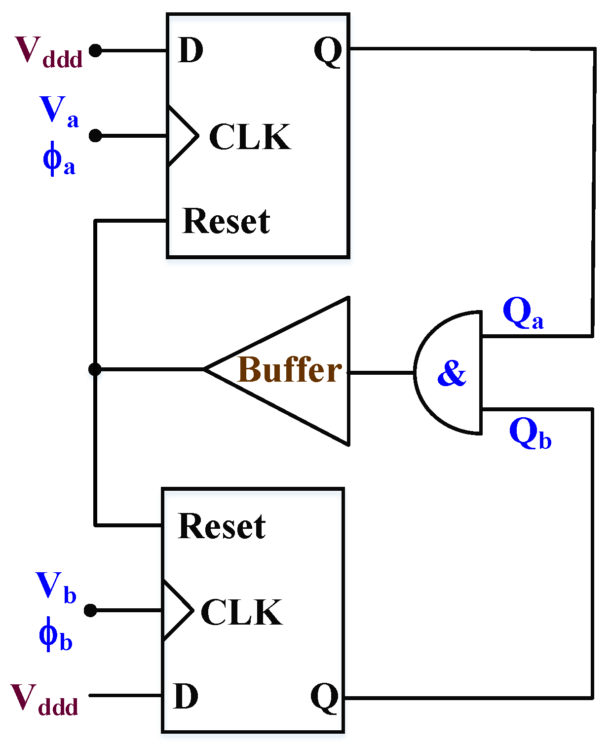
Figure 13 illustrates the adopted PFD, which is composed of two DFFs, a buffer, and an AND gate. If the CLK is triggered by the input reference voltage
Va, then the output
Qa is high because the data (D) are connected to the digital power supply
Vddd. The same mechanism is executed with the feedback voltage
Vb. The PFD used herein can correctly detect the phase difference between φ
a and φ
b. If the phase of φ
a is ahead relative to that of φ
b, a pulse waveform is generated at
Qa, and the pulse width of this waveform is proportional to Δφ. By contrast,
Qb generates a pulse waveform if the phase of φ
b is ahead relative to that of φ
a. A buffer is used to drive the reset signal when both
Qa and
Qb are high.
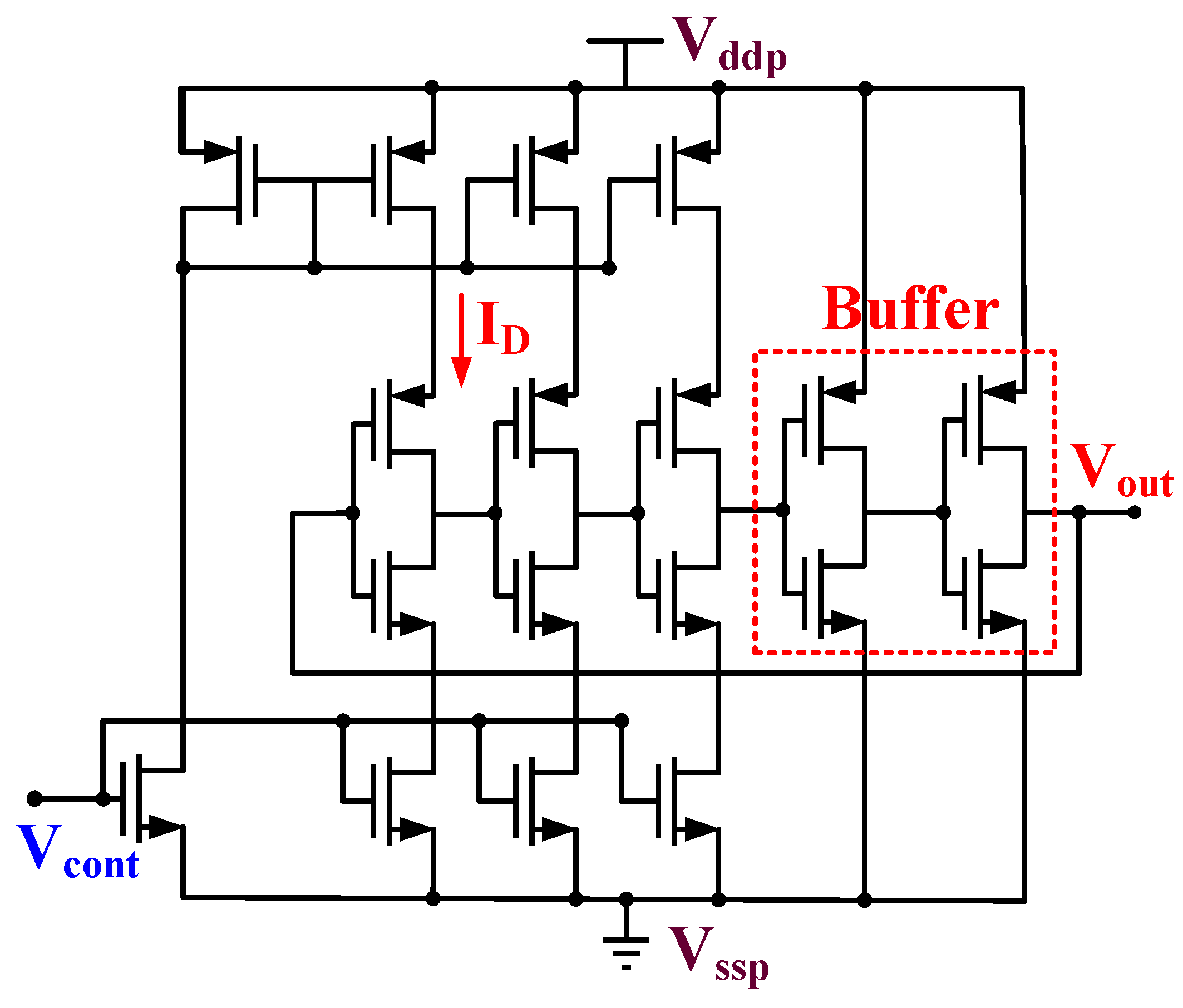
Figure 14 shows the modified three-stage current-starved VCO (CS-VCO) with a buffer, which offers low power dissipation, low phase noise, and high oscillation frequency [
20]. If a certain drain current
ID, number of inverter stages N, and total capacitance
Ctot of a single-stage inverter circuit are known, then the oscillation frequency
fosc can be calculated using the digital power supply
Vddd.
If both
N and
fosc are selected according to the designed CS-VCO, then the drain current
ID can be calculated with (6). The transistor sizes (
W/
L) can then be set based on the aforementioned calculated drain current. A buffer is added to improve the output swing voltage based on the two inverters. There is usually a tradeoff between the output swing voltage and the oscillation frequency. The FD of the PLL is implemented using a six-stage DFF circuit [
21]. The divide ratio of the divider circuit is set to 64. If the output frequency of the CS-VCO is 320 MHz, with a divide ratio of 64, then the feedback frequency
Fdiv is 5 MHz.
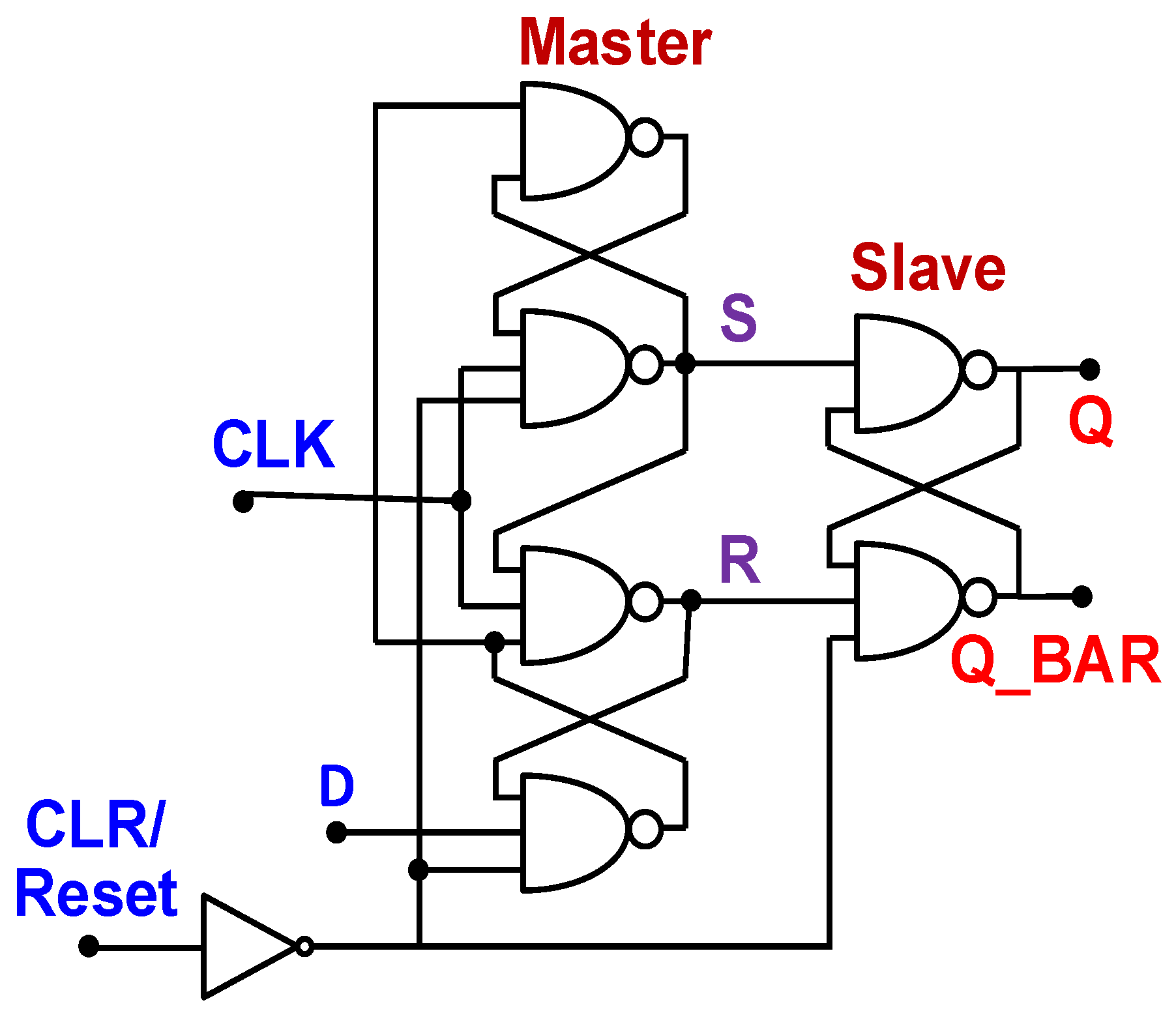
Figure 15 shows the adopted DFF with the asynchronous reset circuit, which is composed of two master R–S latches and a slave latch [
22]. When the reset signal is set to 1, the data (D) and clock (CLK) inputs are simultaneously overridden with a logic low (0). S is then forced to high (1), and R is forced to low (0). The output Q is forced to low (0), and Q_BAR is forced to high (1). Because the rising edge of the clock is used to load the value at the D input, which causes the two master R–S latches to briefly toggle states, the two master R–S latches must be cleared at the same instant. The function of the reset pin should be clean and glitch-free at the outputs Q and Q_BAR. That is, Q should be set to low (0) if it is high (1), and Q_BAR becomes high (1) with almost no skewing.
3. Simulation and Measurement Results
According to (5), the larger the physical dimension
S2,3, the smaller the offset error
Vos. However, the enlarged dimensions of MC
2 and MC
3 reduce the operating speed and increase power consumption. Another method involves adding a serial NMOSFET MC
12 to MC
13, as illustrated in
Figure 9. This design not only reduces the offset error but also enhances the linearity of the modified dynamic comparator. If an offset error
Vos occurs at the input node, then the change in the drain voltage
Fp of MC
4 is significant, and the variation of the gate-to-source voltage Δ
VGS12 of MC
12 is large. However, the drain-to-source voltage
VDS12 of MC
12 varies marginally because MC
12 operates in the saturation mode. The internal voltage
VP thus changes insignificantly. Furthermore, the common-mode input voltage
Vinp of MC
2 is equal to that of
Vp with perfect matching. This design improves the linearity of the modified dynamic comparator.
where
Vinp is the positive input voltage,
Vovi the overdrive voltage of MC
i, and
VGSi is the gate-to-source voltage of MC
i.
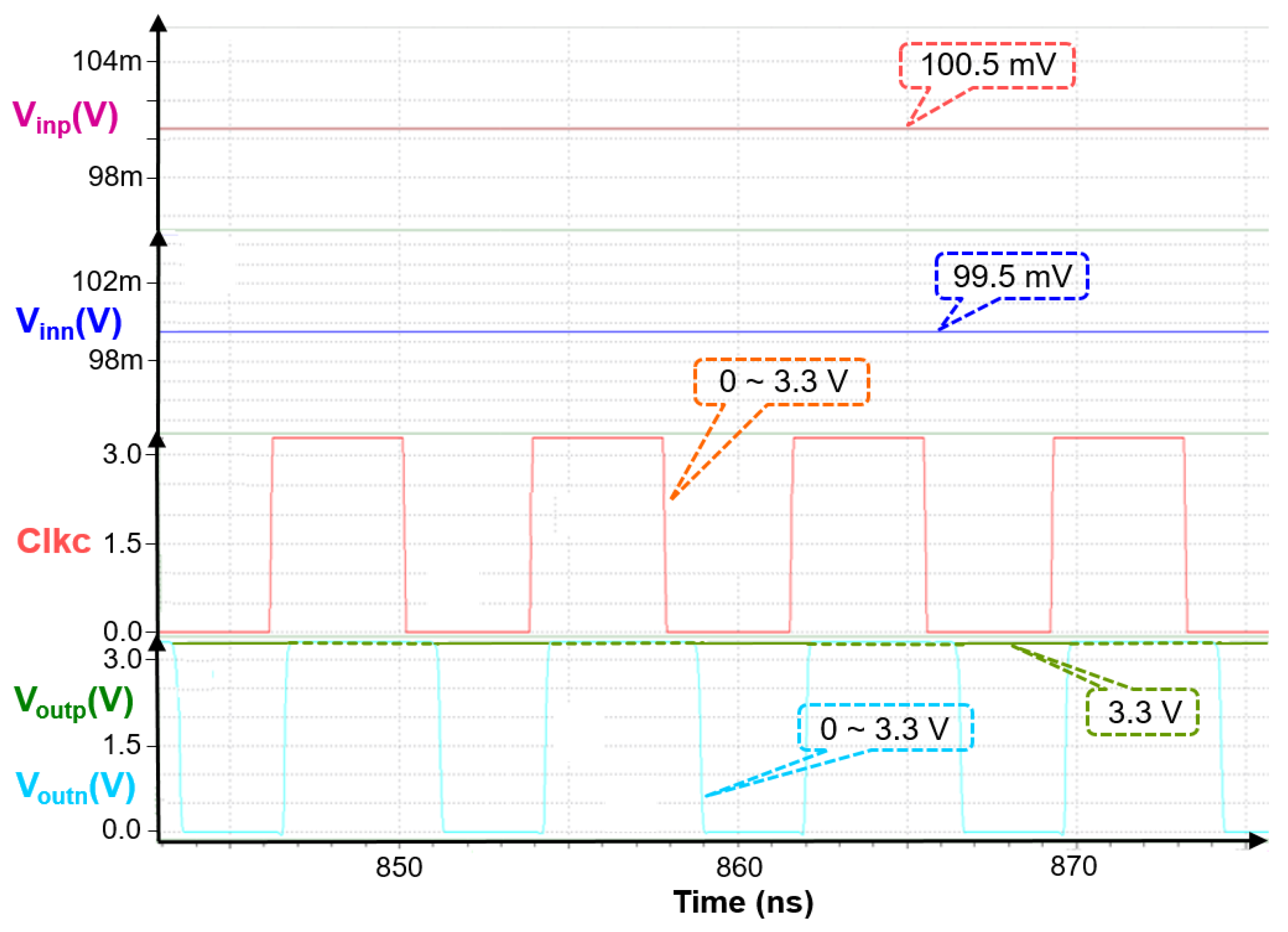
Figure 16 shows the simulated output waveforms of the modified dynamic comparator at a constant common-mode voltage of 100 mV and a differential input voltage of 1 mV. In the 10-bit PLL-SAR ADC, the differential input voltage of 1 mV is approximately 0.25 LSBs. Moreover, the simulated power spectrum density (PSD) shows that the resolution is approximately 12 bits, which fulfills the requirement of the 10-bit PLL-SAR ADC.
Figure 17 and
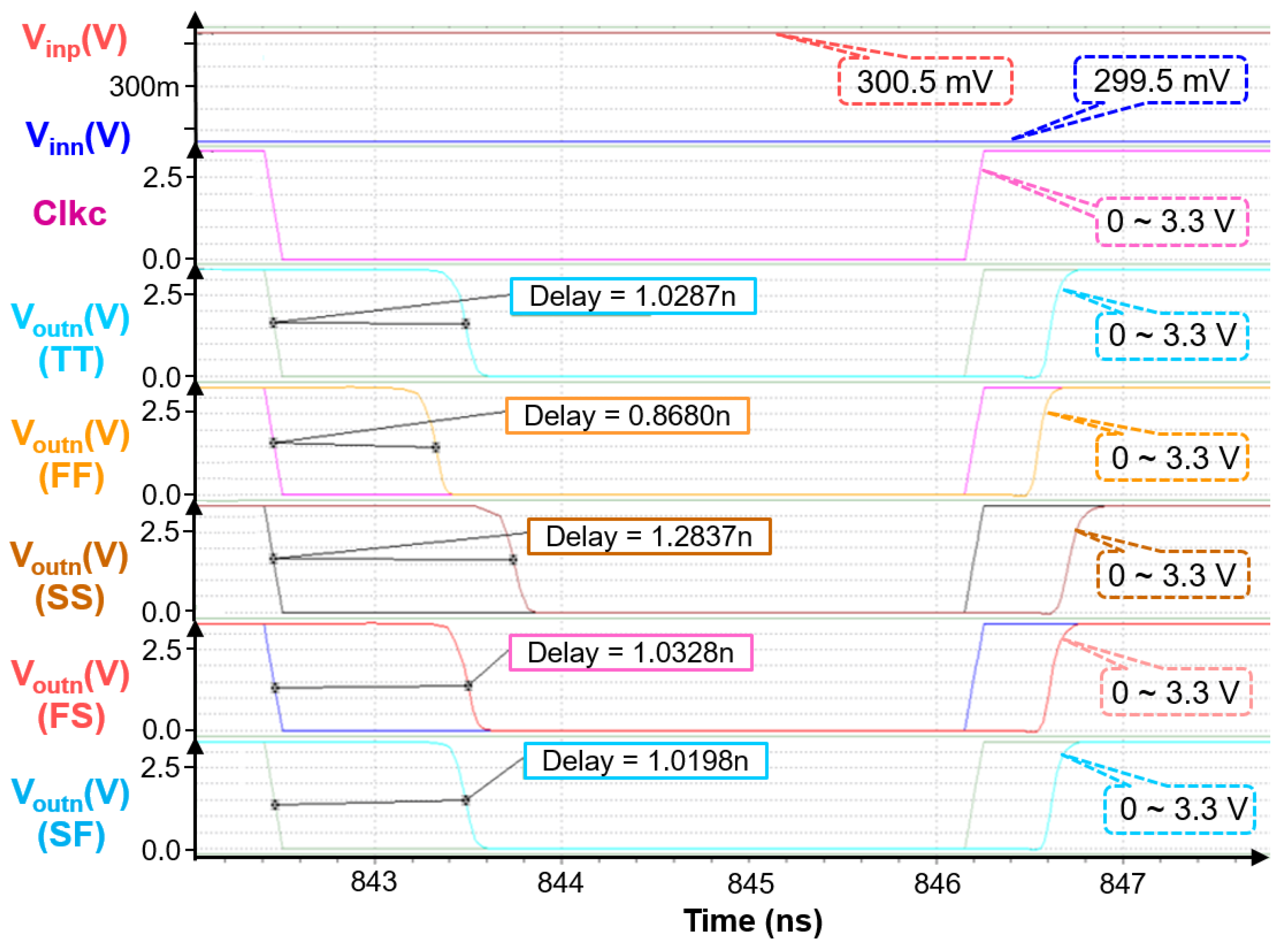
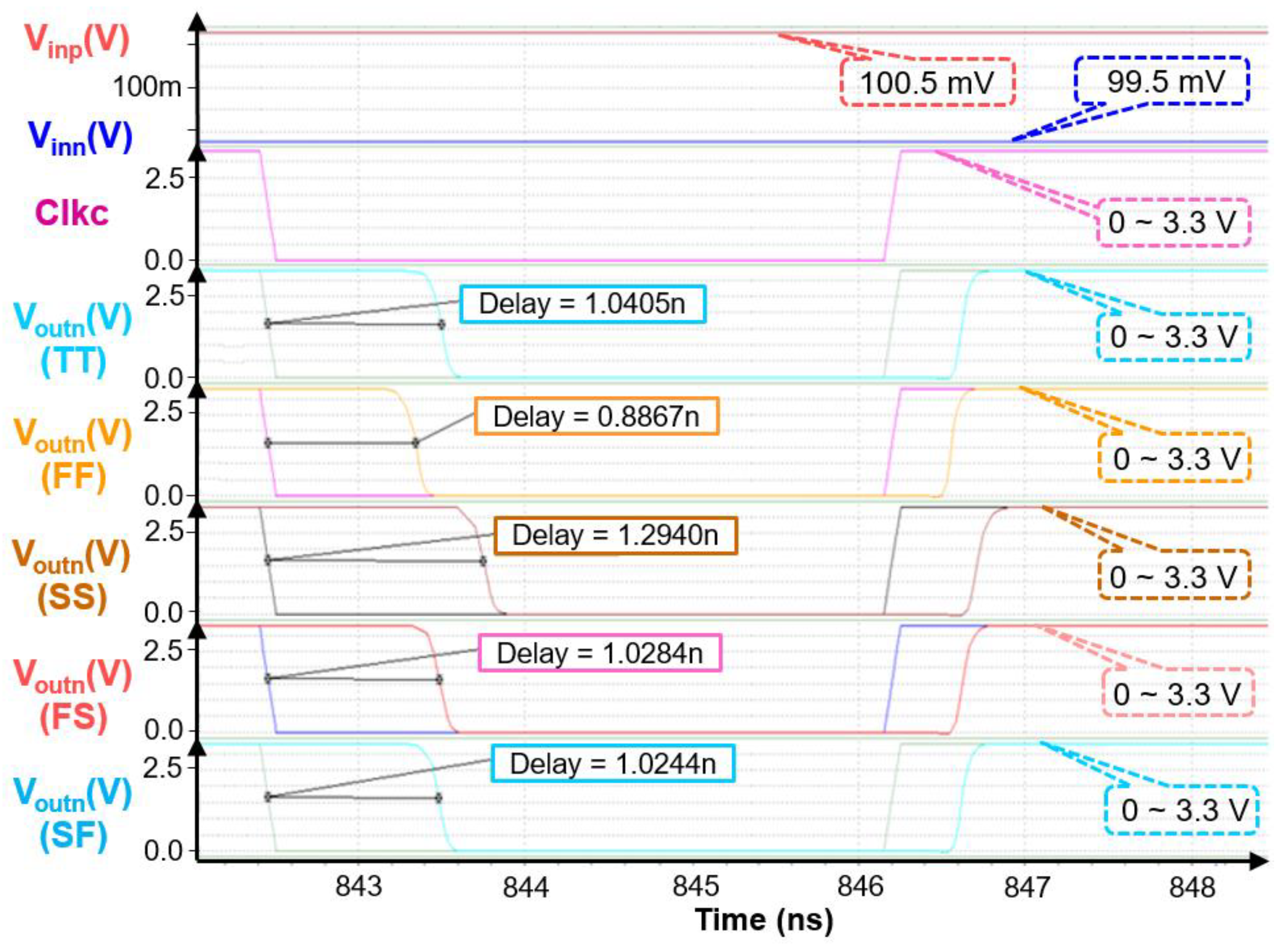
Figure 18 illustrate the propagation delays at five process corners with two common-mode voltages of 300 and 100 mV, respectively. Notably, the propagation delays between FF and SS at the common-mode voltages of 300 and 100 mV are of 415.7 and 407.3 ps, respectively. These values imply that the aforementioned propagation delays are nearly constant and are unrelated to the common-mode voltage.
As shown in
Figure 2, the clock signal
CLKs is used to control the switching states of the DAC switches S
0–S
10 and generate a comparison signal
Clkc after its passage through the SAR control logic. Because
Clkc is low, the comparison function is executed in the proposed dynamic comparator, and the reset function is activated.
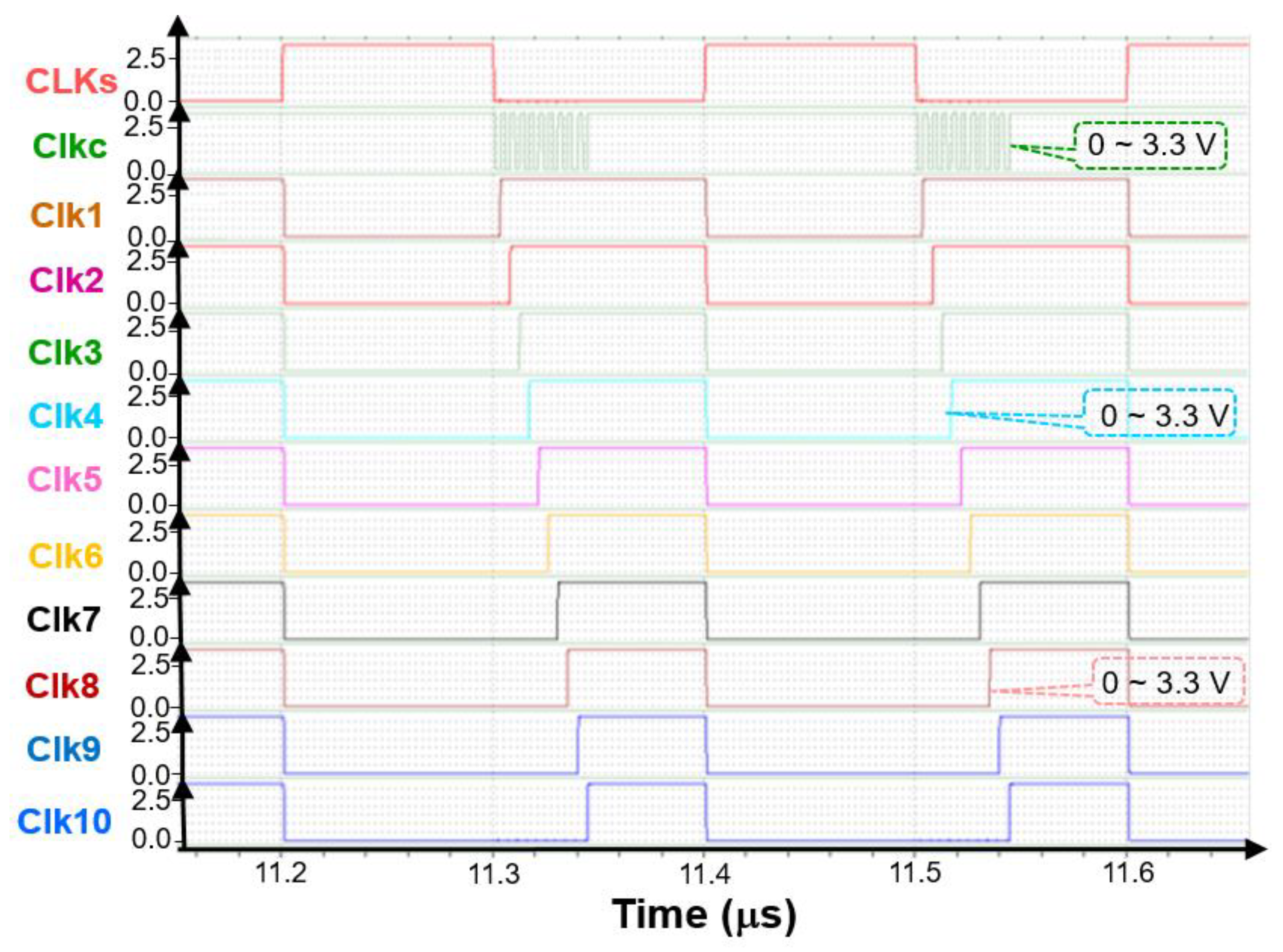
Figure 19 shows the simulated waveforms of the asynchronous control logic circuit.
As shown in
Figure 12, a six-stage DFF circuit was used to implement an FD for the PLL. The divide ratio of the divider circuit was set to 64.
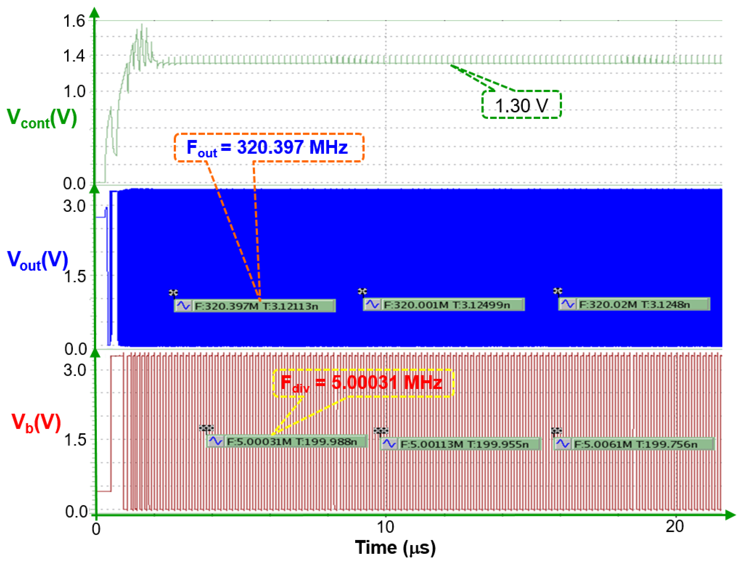
Figure 20 shows the simulated waveforms of the adopted FD at the control voltage
Vcont of 1.30 V. The output frequency
Fout of CS-VCO was 320.397 MHz, and the resulting feedback frequency
Fdiv was 5.00031 MHz. Thus, the simulated divide ratio was approximately 64.075, which is close to the theoretical value of 64. These simulated results indicate that the designed FD circuit works correctly. The feedback frequency
Fdiv of 5.00031 MHz is fed to the clock signal
CLKs in the S/H circuit and the asynchronous SAR control logic circuit, as illustrated in
Figure 2.
Figure 21 illustrates the post-layout simulated PSD of the proposed PLL-SAR ADC. According to the 32,768-point FFT simulation, the simulated SNDR was 58.23 dB, which is equal to 9.38 bits, at the input frequency of 200 kHz, sampling frequency of 5 MS/s, power supply of 3.3 V, and power consumption of 1256 μW.
Table 2 summarizes the post-layout simulated results of the proposed PLL-SAR ADC with three design corners, namely typical (TT), fast (FF), and slow (SS). The simulated DNL located between the −1.23 and +1.81 LSBs and the INL located between the −1.22 and +1.81 LSBs at the TT corner based on the input voltage varied from 0 to
VDD. The simulated resolution satisfied the PWM channel with an 8-bit resolution [
23] and a 10-bit ADC [
24] for BLDC motor control applications. Unfortunately, the DNL and INL perform with missing code because they are larger than 1.0 LSB.
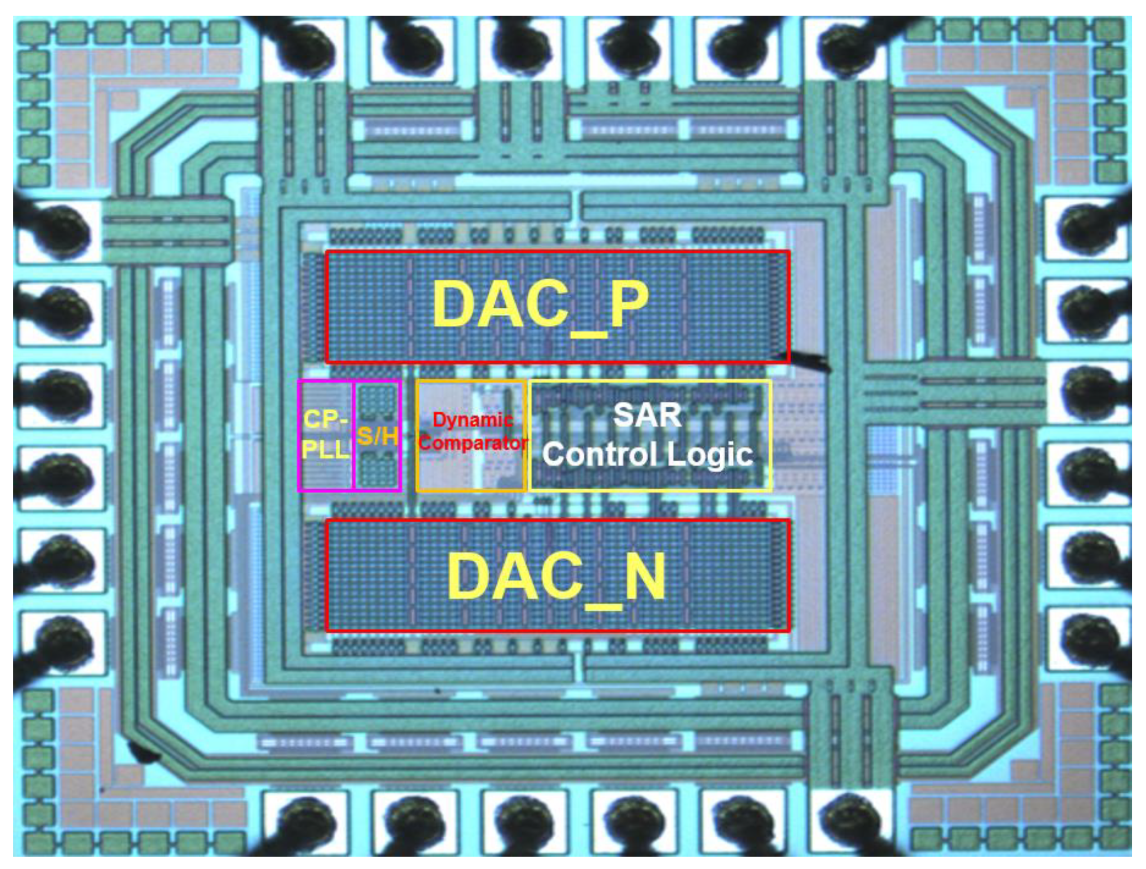
Figure 22 shows a chip microphotograph of the proposed PLL-SAR ADC. A separation alignment is considered to divide the large capacitor into two small capacitors and place them symmetrically. The small capacitor is placed at the center of the circle, whereas the large capacitor is in alignment outside of the circle. The parasitic impedance and capacitance can be reduced through adoption of a symmetric layout. Furthermore, temperature variation does not affect the resolution of the proposed SAR ADC between −40 and 100 °C.
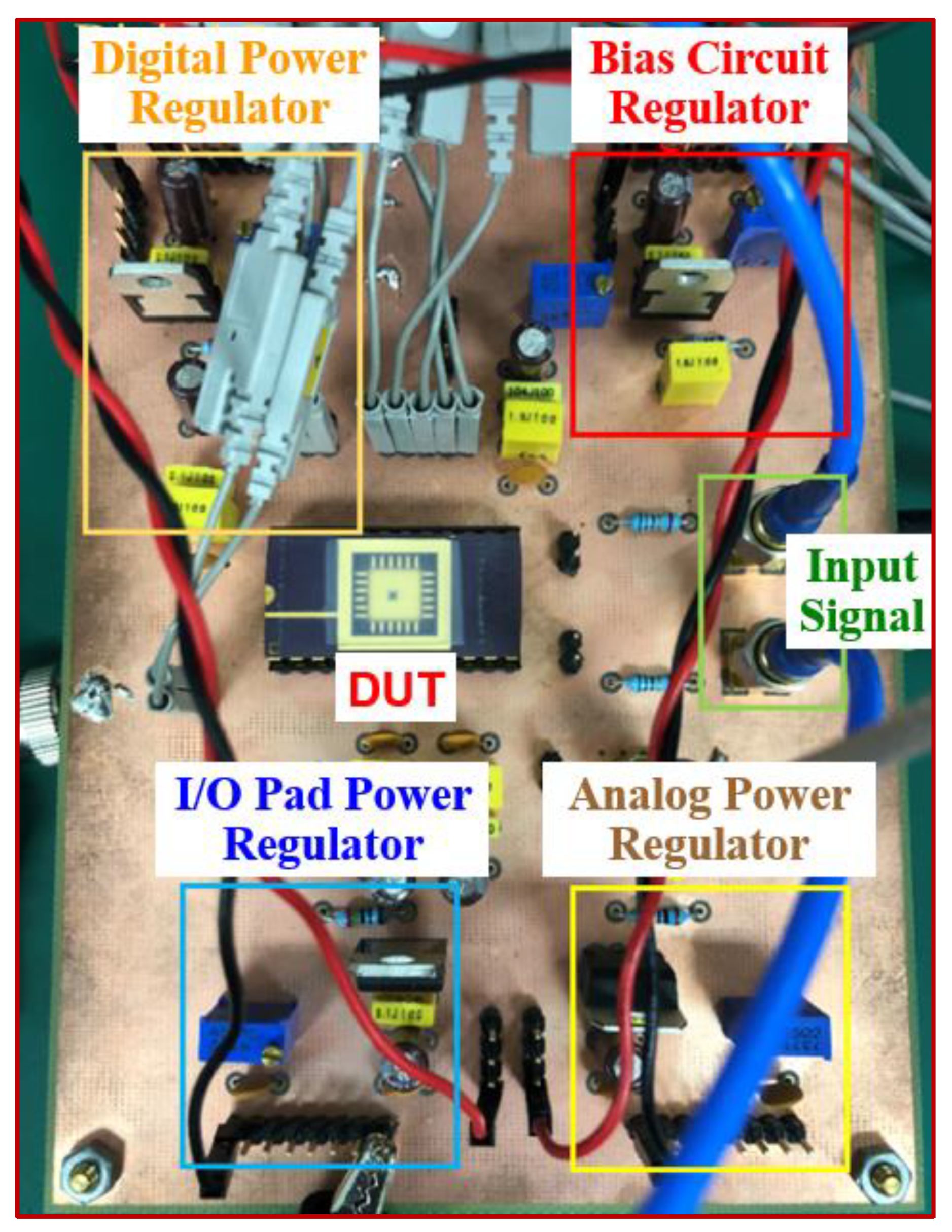
Figure 23 presents the measured printed circuit board (PCB) of the proposed PLL-SAR ADC with the device under test (DUT). The function generator (SRS DS360, Harpenden, UK) provided an input frequency of 200 kHz, the pulse data generator (Agilent 81130A, Ferrara, Italy) generated a clock frequency of 5 MS/s, and the power supply (Keysight E3631A, Santa Rosa, CA, USA) and reference voltage (Keysight N6761A, Santa Rosa, CA, USA) provided a power supply of 3.3 V and bias voltage of 2.25 V, respectively. The digital output code was captured with a logic analyzer (Agilent 16902B, Ferrara, Italy) and imported into the MATLAB environment to calculate the SNDR and ENOB. The digital power, bias power, I/O pad power, and analog power were separated to prevent power interference in the DUT, which was mounted onto the PCB. Many three-terminal adjustable voltage regulators LM317 can supply more than 1.5 A over an output voltage range of 1.25–37.0 V. This includes current limiting, thermal overload protection, and safe operating area protection [
25].
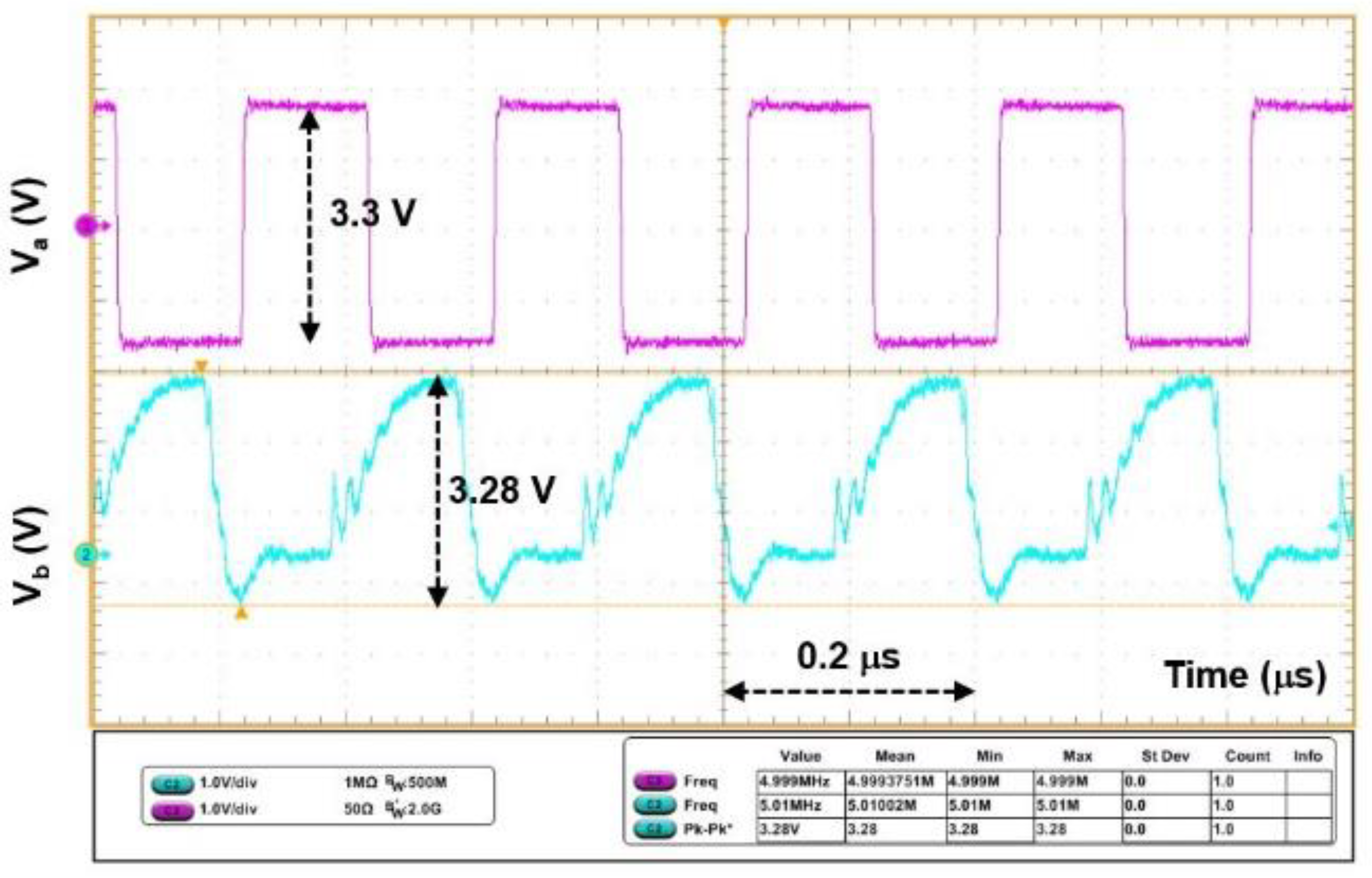
Figure 24 illustrates the measured waveforms of input signal and feedback signal of the proposed PLL. The magnitudes of the input signal
Va and the feedback signal
Vb are 3.3 V and 3.28 V, respectively, at the sampling frequencies of 4.999 MHz and 5.01 MHz. The measured results also prove that the proposed PLL works successfully. Because of the correct PLL design, an internal clock signal of the PLL (
PLLout) is provided to guarantee that a correct clock signal (
CLKs) is obtained. That is, this study does not directly use the reference 5 MHz signal as the CLKs.
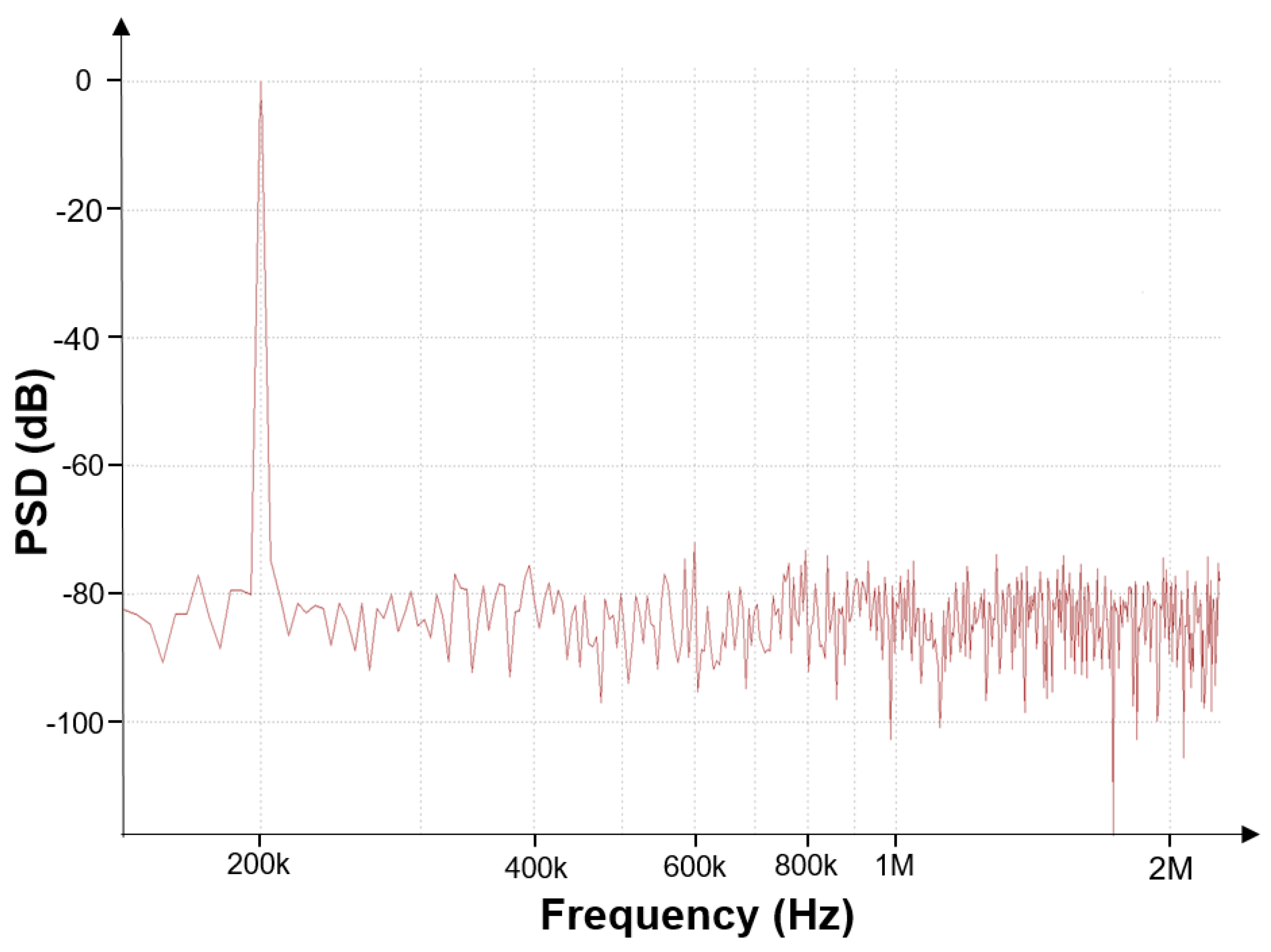
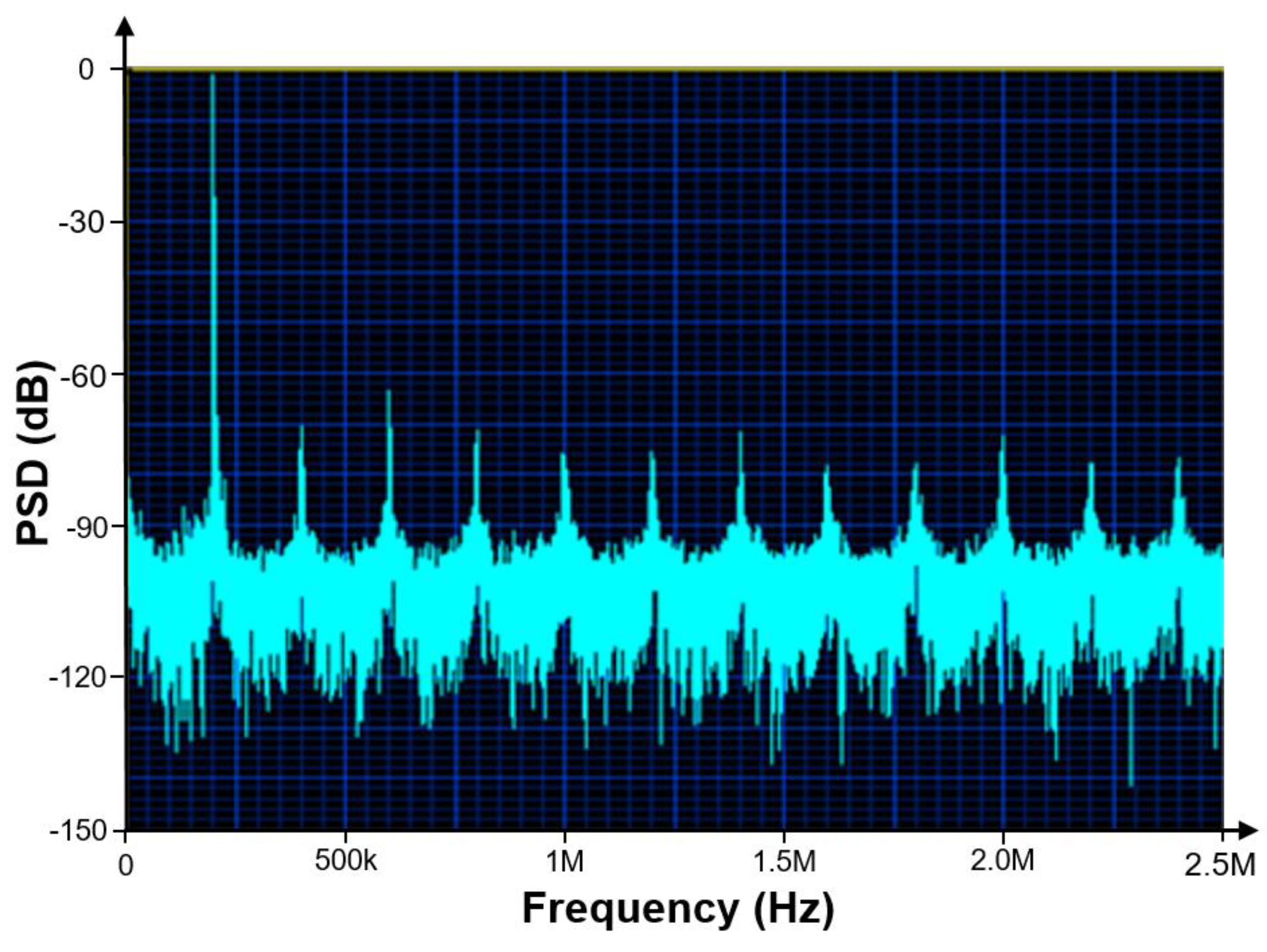
Figure 25 presents the measured output 32,768-point PSD of the proposed PLL-SAR ADC at the input frequency of 200 kHz, sampling frequency of 5.0 MS/s, power supply of 3.3 V, and reference voltage of 2.25 V. When a full-scale input sine wave was considered at the input frequency of 200 kHz, the proposed PLL-SAR ADC yielded an SNDR of 53.82 dB, which was approximately 8.65 bits. The measured ENOB of 8.65 bits is inferior to the simulated ENOB of 9.45 bits. The reason is that the output voltage performs with nonlinearity in capacitive DAC. Fortunately, the measured resolution of 8.65 bits fulfills the specification of the PLL-SAR ADC in the BLDC motor drive because the PWM register contains an 8-bit channel with clock frequencies of 0.25–8.0 MHz [
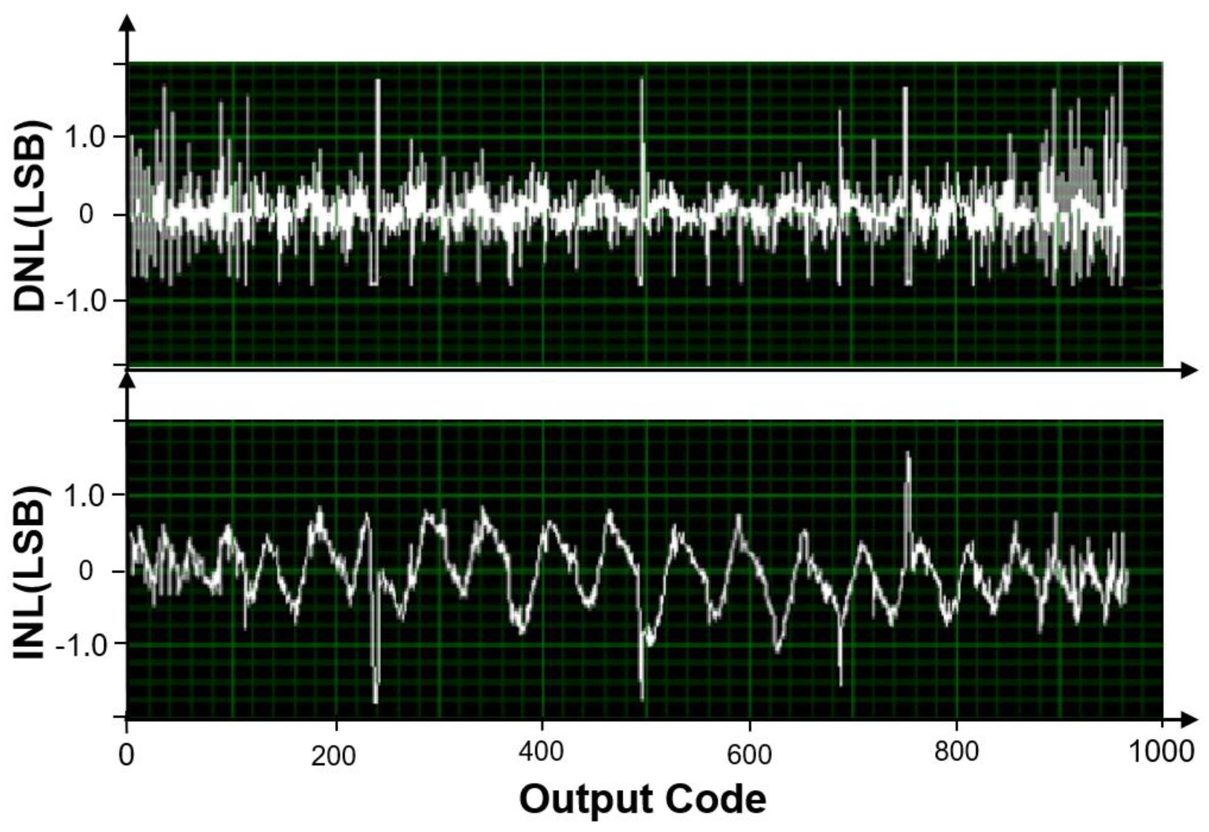
24]. The DNL and INL are depicted in
Figure 26. The measured DNL varied from −0.80 LSB to +1.94 LSB, and the measured INL varied from −1.80 LSB to +1.62 LSB. The proposed PLL-SAR ADC operated with missing code because the measured DNL and INL were larger than 1.0 LSB. Fortunately, most of the measured DNL and INL values varied from −1.00 LSB to +1.00 LSB, and the few relatively large INL/DNL values can be attributed to the parasitic capacitance and the clock feedthrough phenomenon from the N- and P-type input stages. Moreover, the second-order effects such as channel-length modulation and mismatch effects inside the S/H circuit must be addressed in future studies [
26].
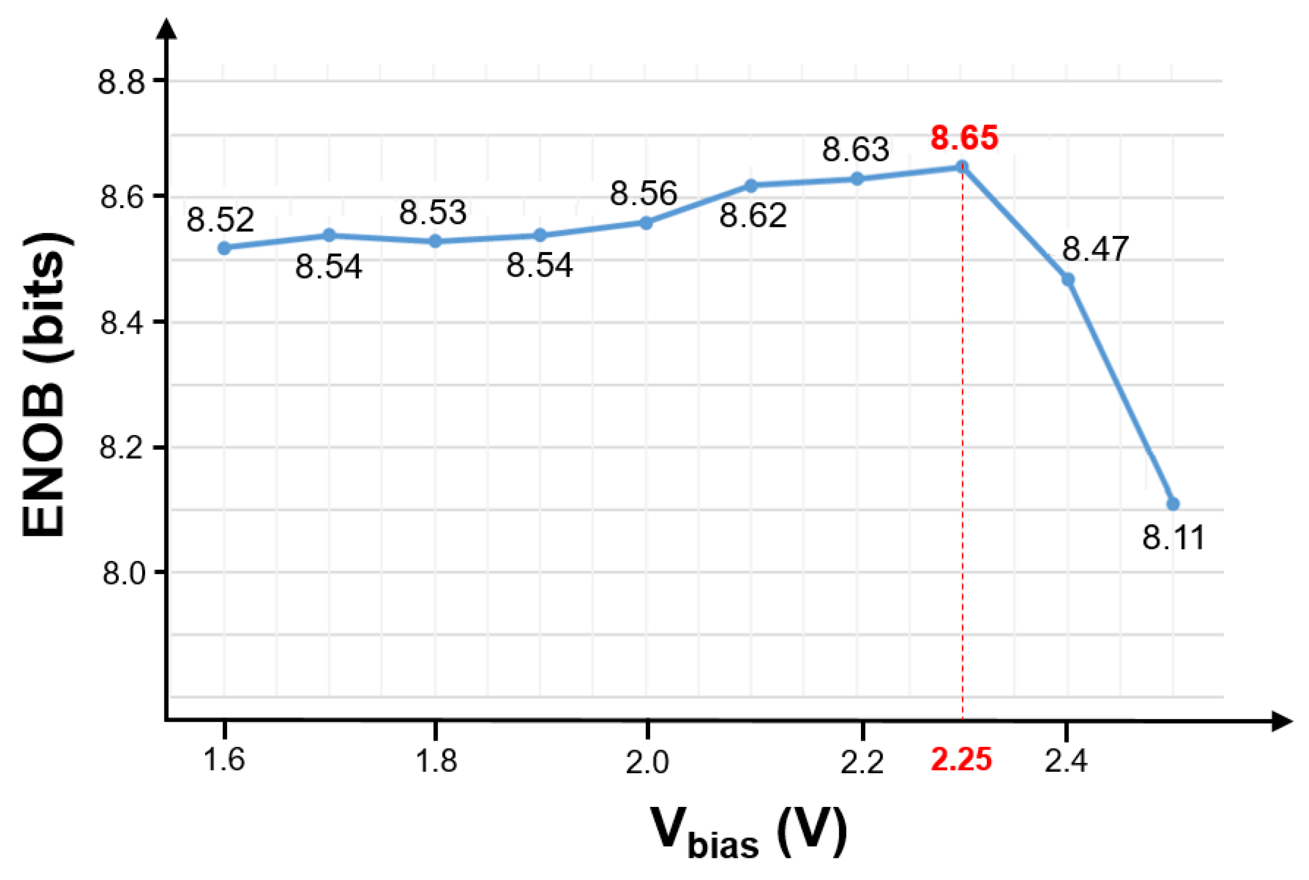
Figure 27 shows the measured ENOB with respect to the bias voltages of 1.6–2.4 V at the input frequency of 200 kHz and sampling frequency of 5.0 MS/s. The measurements for the ENOB were uniform from 1.6 to 2.25 V, and the maximum ENOB of 8.65 was observed at 2.25 V. The ENOB decreased sharply when the bias voltage exceeded 2.25 V. As summarized in
Table 2, the post-layout simulated SNDR of 58.23 dB can be compared with the measured SNDR of 53.82 dB. The difference is small because the modified two-stage dynamic comparator can prevent kickback noise, whereas the modified S/H circuit reduces the clock feedthrough with a dummy switch and eliminates charge injection with a dummy transistor.
All characteristics of the proposed 10-bit 5-MS/s PLL-SAR ADC with modified bootstrapped switch for BLDC motor drive were successfully verified.
Table 3 summarizes the measured properties of the proposed PLL-SAR ADC developed herein and compares them with those of other SAR ADCs. The performance comparison proved that the power consumption of this chip is lower than that of the SAR ADCs developed in [
7,
27] and that the measured ENOB in this study is superior to that reported in [
7,
13,
28]. The proposed CDAC consumes a power of 660 μW, which is approximately 52.5% of total power consumption. Furthermore, the FoM of 0.625 pJ/conv-step measured in this study is superior to the reported value of 3.317 pJ/conv-step in [
13], 7.403 pJ/conv-step in [
27], and 30.873 pJ/conv-step in [
28]. Notably, the proposed PLL-SAR ADC achieves the highest sampling rate (5.0 MS/s). Unfortunately, the measurements for the DNL and INL of this study were inferior to those of the compared SAR ADCs. The post-layout simulated SNDR was 58.23 dB, which is equivalent to an ENOB of 9.38, whereas a lower ENOB of 8.65 was measured for our implemented chip. That is, the chip fabricated in this study is affected by nonlinear CDAC, clock feedthrough error, process variation, and thermal noise.


