Abstract
Hot carrier injection (HCI) can generate interface traps or oxide traps mainly by dissociating the Si-H or Si-O bond, thus affecting device performances such as threshold voltage and saturation current. It is one of the most significant reliability issues for devices and circuits. Particularly, the increase in heat generation per unit volume due to high integration density of advanced integrated circuits leads to a severe self-heating effect (SHE) of nanoscale field effect transistors (FETs), and low thermal conductivity of materials in nanoscale FETs further aggravates the SHE. High temperature improves the HCI reliability in the conventional MOSFET with long channels in which the energy of carriers can be relaxed. However, high temperature due to severe SHE deteriorates HCI reliability in nanoscale FETs, which is a big concern in device and circuit design. In this paper, the modeling and simulation methods of HCI in FETs are reviewed. Particularly, some recently proposed HCI models with consideration of the SHE are reviewed and discussed in detail.
1. Introduction
Hot carrier injection (HCI) is a significant reliability issue for transistors in analog/RF circuits and logic circuits [1,2,3,4,5,6]. Considerable evidence show that hot carriers can dissociate the Si-H and Si-O bond through a single-carrier process or multiple-carrier process [7,8,9,10,11,12]. As a result, interface traps and oxide traps are generated [13], which leads to the degradation of transistor performance, such as threshold voltage shift (), mobility shift (), linear current shift (), saturation current shift () and transconductance shift () [2,14,15,16,17]. Furthermore, the degradation of transistor performance degrades the performance of the circuit. For example, it can increase the risetime in inverters [18]; increase the delay for large-scale digital circuits [19,20], which reduces the maximum frequency of the CPU; and it also causes the read disturbance of memory [21] and increases the probability of failure of the memory system [18,22].
Various models have been developed to reveal the physical mechanisms behind the phenomena, and models were also built to predict HCI induced device degradation. In 1985, Hu et al. developed the lucky electron model involving Si-H bond breakage and related HCI with the maximum electric field in the channel, based on which the time dependence of interface traps can be derived and the barrier energy for creating interface traps can also be extracted [7]. In 1995, the behavior of hot-carrier-induced degradation of deep-submicron n-Channel LDD MOSFETs was modeled analytically by introducing an empirical model of mobility degradation and series resistance [23]. In 2002, Mcmahon et al. proposed a model for interface trap generation through multiple vibrations of electrons: the model relates the device lifetime with the magnitude of source-drain current, and large source-drain current increases the probability of multiple vibrations of electrons and degrades the device faster [8]. In 2005, Rauch et al. proposed an energy-driven paradigm to describe hot carrier behavior in scaled NMOSFETs of that time, in which the available electron energy, instead of the peak lateral electric field in the lucky electron model, is the fundamental “driving force” for HCI [24]. In 2009, a theoretical framework for interface state creation by dissociation of Si-H bonds at the Si/SiO2 interface was developed by Guerin et al. [9], which includes three main ways of bond breaking: the first one is due to the rising of energy levels because of strong quantum confinement caused by a large electrical field, the second one is due to very energetic incident carriers, the third one is due to numerous but less energetic carriers. In 2014, Bina et al. presented and verified a physics-based model of hot carrier degradation (HCD) based on a thorough solution of the Boltzmann transport equation [25], which is capable of representing HCD in transistors stressed under different conditions using a unique set of model parameters. In 2016, Chen et al. developed a numerical simulation method to capture HCI induced threshold voltage shift with consideration of time-dependent temperature in SOI MOSFETs [26] and FinFET [27], which is applicable to analyze HCI for transistors under stress voltage with different duty cycles, frequency and waveform. In 2017, Jiang et al. proposed an analytical model to capture the temperature of transistors in a digital circuit that is biased under pulse trains characterized by frequency and power duty cycle, then HCI performance is predicted [28]. Yu et al. proposed a trap-based compact model [29,30,31], which can accurately predict hot carrier degradation and variation in full Vgs/Vds bias. In 2019, a SPICE compatible compact hot carrier degradation time kinetics model was proposed for conventional, lightly doped drain, and drain extended MOSFETs and FinFETs [32]. In 2022, Wang et al. introduced the artificial neural network (ANN) method into HCI reliability prediction and significantly reduced the HCI simulation cost [33].
In the conventional long-channel MOSFET, the worst case HCI condition is VG = VD/2 in which reaches maximum [2]. The traps generated by HCI are located at drains corresponding to maximum lateral electric field [34]. The time evolution of degradation follows the power law. In short-channel MOSFET, the worst HCI condition is VG = VD [35]. The traps generated by HCI are closed to source and drain [36,37]. The time evolution of degradation follows the power law in the early time and becomes saturated at long time stress. In FinFET, two types of oxide traps and interface traps are generated [29]. The oxide traps generated in planar devices only have one type [29]. The difference can be explained in that FinFET has one more lattice orientation than the planar device [30]. The interface traps and oxide traps (type 1) are mainly located at the channel center closer to the source on the Fin sidewall, while the oxide traps (type 2) are mainly distributed at the channel center closer to the drain on the Fin top [30]. In gate-all-around (GAA) nanowire, HCI is dependent on its width [38,39]; the degradation mechanism is similar to that of the planar device but the self-heating effect becomes more severe and needs to be taken into account [40].
Moreover, HCI in nanoscale FET deteriorates as temperature increases [3,41,42,43], which is totally different from the conventional long-channel MOSFET [44,45,46,47,48]. One explanation is that the bond dissociation in nanoscale FET is more triggered by multi-vibration excitation (MVE) than single-vibration excitation (SVE) [49] and high temperature favors bond dissociation rate [42,50,51]. Another explanation is that the total HCI consists of two parts: classical channel hot carrier (CHC) at the drain side and bias temperature instability (BTI) along the channel [37,52]. As the temperature increases, the increase in BTI degradation is greater than the decrease in CHC degradation; consequently, the total degradation increases with temperature [52].
On the other hand, a more severe self-heating effect (SHE) in nanoscale transistors happens because of the increase in heat generation per unit volume caused by high integration density [53]. Furthermore, low thermal conductivity of the more confined thin films in silicon-on-insulator (SOI) MOSFET and FinFET leads to more severe SHEs [54,55,56,57]. As a result, the temperature in nanoscale transistors increases significantly [58,59,60,61]. Severe SHE further deteriorates HCI reliability for nanoscale transistors, which is a big concern in modern nanoscale transistors [3,41,42,50,62].
The review paper is organized as follows: In Section 2, we present and discuss some recently proposed modeling and simulation methods for HCI, including numerical methods [26,27,33], an analytical HCI model in digital circuit [3,28,63], trap-based HCI models [29,30,31] and an ANN model for HCI reliability [33]. In Section 3, a conclusion and outlook are given.
2. Modeling and Simulation Methods
2.1. HCI Simulation via Numerical Methods
In order to calculate the HCI-induced threshold voltage shift under stress voltages with different waveforms and frequencies, numerical simulation methods were developed for SOI MOSFETs and FinFETs [26,27,33]. The simulation process can be divided into three parts: (1) the current density can be obtained by numerically solving carrier transport equations, then the time dependent heat generation rate for the device under different stresses voltage can be obtained; (2) by using a numerical method to solve the time-dependent thermal conduction equation, the transient temperature responses can be obtained [26,27,33]; (3) HCI induced threshold voltage shift (TVS) as a function of time is then captured numerically based on the temperature response [26,27,33]. The numerical methods can simulate HCI under various stress voltages and operation conditions. However, the simulation cost is high, which makes it very time-consuming to calculate TVS for a long-time stress, and thus extrapolation is typically applied.
2.1.1. Electro-Thermal Numerical Simulation
The time-dependent temperature distribution is obtained by solving the heat conduction equation,
where is the density of materials, is the specific heat capacity of materials, is the temperature, is thermal conductivity, which depends on materials and temperature, and is the heat generation rate. Following the standard procedure of the time domain finite element method [64,65,66], the matrix form of Equation (1) can be obtained,
where is the time-dependent matrix, is the thermal conduction matrix, is the overlap matrix, is the boundary condition matrix, is the heat generation vector and is the time step for time evolution.
The current density in 100 nm SOI MOSFET with device structure, as in [26], can be obtained by solving the Poisson Equation (3), drift-diffusion Equations (4) and (5) and current continuity Equations (6) and (7):
where is the voltage; n and p are the electron and hole density, respectively; and are the donor and acceptor density, respectively; and are the relative dielectric and constant vacuum dielectric constant, respectively; and , , and are the electron (hole) current density, mobility, diffusion coefficient and generation rate, respectively, where , , and are holes. The heat generation in the SOI MOSFET then can be written as,
where and are the current density and the electric field intensity, respectively.
On the other hand, for the advanced short-channel field effect transistor in which the quantum transport rather than drift-diffusion transport should be considered, it is quite difficult to obtain the heat generation rate by simulating the quantum transport process with carrier scattering; therefore, Gaussian distribution is usually applied to model the heat generation rate in short channel devices [27,67,68]. Take FinFET as an example. Figure 1a shows the 3D schematics of a 3-Fin 14 nm n-type FinFET, including the source extension, source, channel, drain and drain extension [67,69,70]. The cross sections of the FinFET perpendicular to and parallel to the channel are shown in Figure 1b,c, respectively [33]. The heat generation rate along the channel direction in this FinFET is shown in Figure 2 [33].
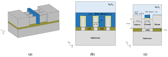
Figure 1.
(a) The 3D schematics of the 14 nm technology node n-type FinFET [33], (b) the cross section perpendicular to the channel (y-z plane) [33], and (c) along the channel (x-z plane) of the FinFET [33].
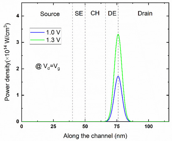
Figure 2.
Gaussian distribution is applied to model the heat generation rate along the channel for FinFET [33].
2.1.2. Temperature-Dependent Threshold Voltage Shift (TVS) Model
To simulate TVS under time-dependent temperature, TVS can be numerically calculated by [26,27,33],
where is the device threshold voltage shift, is time step and is the time interval between two adjacent time steps. is the TVS model under DC voltage stress and usually varies for different device types. A temperature-dependent parameter is introduced for calculating the TVS for SOI MOSFET, and the TVS as a function of time with linear temperature-dependent parameters can be expressed as [26,71],
where is the temperature-dependent parameter and is stress time. Equation (9) then can be rewritten as,
Furthermore, a Vd and Vg dependent term is included into Equation (12) to simulate the TVS under real circuit stress [27],
where and are the gate voltage and drain voltage at time step , respectively.
In order to capture the saturation behavior of TVS evolution, an empirical model to capture the saturation behavior of TVS evolution for 14 nm FinFET is applied [29,33],
where is maximum TVS, associates with bond dissociation rate, is the exponent of TVS at power law stage and and are time-dependent for a time-dependent stress voltage and can be expressed as [32],
where and are the gate and drain voltage, respectively; is the temperature of the device; is the Boltzmann constant; is the activation energy depending on device type and scale; , and A are coefficients; and are fixed parameters for all devices; and is a device-specific parameter. The derivative with respect to time for Equation (14) can then be obtained [33],
2.1.3. Simulation Results
The I-V curve of SOI MOSFET is obtained by solving the Poisson equation, drift-diffusion equations and current continuity equations [26]. The transient temperature responses for different voltage stress are then calculated as shown in Figure 3a,b [26]. The simulation results in [25] show: (1) the step pulse has much higher temperature response than the AC pulse and pseudo-random binary sequence (PRBS) pulse due to higher input power; (2) the temperature oscillations of the PRBS pulse and low frequency pulse are larger than those of the AC pulse and high-frequency stress, respectively. The PRBS pulse has consecutive On (1.2 V) and Off (0 V) states and the low-frequency AC pulse has a longer On state time, so they have a more time for the temperature to increase or fall.
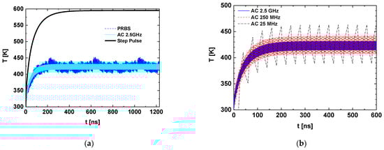
Figure 3.
Temperature response in linear time scale to (a) different signal voltage stresses of AC signal (cyan), PRBS signal (blue) and step pulse (black); (b) AC signals with different frequencies of 2.5 GHz (blue), 250 MHz (red) and 25 MHz (black) [26].
Based on the temperature response, the TVS under different waveforms and frequencies is further captured as shown in Figure 4a,c [26], respectively. Some trends for a single transistor under different biases can be concluded: (1) as the frequency decreases, the TVS increases; (2) PRBS stress suffers more severe HCI than AC stress at the same frequency [26]. The above-mentioned conclusion is also validated by experiment data [3,15,42,43,60].
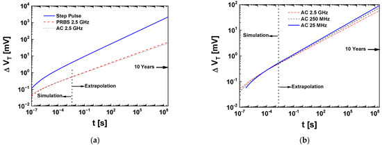
Figure 4.
Simulated threshold voltage shift ΔVT as a function of time for (a) step pulse, 2.5 GHz PRBS and AC pulse, (b) 2.5 GHz, 250 MHz and 25 MHz AC pulse [26].
2.2. Analytical HCI Model
An analytical model for calculating self-heating peak temperature for digital circuits has been proposed and validated [28]. The HCI lifetime can then captured by inserting the peak temperature into the analytical HCI model [3,28]. The thermal resistance is an average value and the simulation accuracy is not as high as that of numerical simulation. In order to acquire high accuracy, an equivalent thermal circuit model can be established by carefully dividing the simulation region into several sub-domains.
2.2.1. Temperature Prediction via Thermal Equivalent Circuit
The self-heating peak temperature by using the thermal equivalent circuit can be expressed as follows [28]:
where is the difference between the maximum temperature () and average temperature (); , and are thermal resistance, capacitance and time constant, respectively; and are the maximum and average value of the dissipated function over time; and are the frequency and duty cycle of signal; and is used to calculate and can be viewed as a differential thermal resistance.
2.2.2. HCI Prediction
The HCI degradation can be captured by introducing the temperature calculated from Equation (19) into the TVS model [28]:
where is the threshold voltage shift; is the stress time; is lattice temperature; is the voltage between drain and source; and , and are accelerator factor, time exponent and activation energy, respectively, which are technology- and device-specific parameters [60].
In order to predict the HCI lifetime of the circuit, the lattice temperature in the summarized HCI model Error! is replaced by peak temperature (), which can be expressed as
where is the environment temperature and is calculated by Equation (18) [28].
2.2.3. Application and Simulation Results
A ring oscillator (RO) with variable order of inverter (), loaded by the same capacitor , was investigated [28], and the peak self-heating temperature is shown in Figure 5a [28]. The symbol is the HSPICE simulation results while the solid line was calculated via the analytical model mentioned in Section 2.1.1 [28]. increases linearly with frequency mainly because increases linearly with frequency and leads to increasing linearly with frequency, as shown in Figure 5b [28]. In contrast, and both decrease with frequency [28]. As a consequence, at frequencies higher than the technology-specific transistor frequency, which indicates that excess degradation caused by is negligible [28].
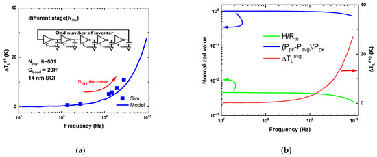
Figure 5.
(a) The peak self-heating temperature increases as the oscillation frequency increase, (b) The explanation of (a) [28].
Figure 6a plots the predicted by Equation (22) for low frequency FinFET and 5 order ring oscillator composed of 90 nm with operated at [28]. Figure 4b illustrates the TVS of FinFET as a function of frequency after 10 years’ operation in RO circuits [28]. The degradation increases with frequency due to higher peak temperature, as shown in Figure 5 [28].
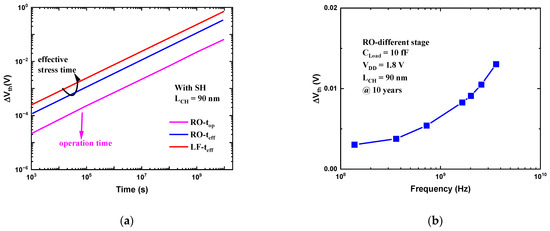
Figure 6.
(a) Predicted time evolution for a low-frequency (LF) MG-FET under HCI stress and in RO circuit; (b) the TVS of FinFET as a function of frequency after 10 years’ operation in RO circuits [28].
2.3. Trap-Based HCI Model
Typically, HCI are modeled by investigating the carrier transport process, such as the lucky electron model or the energy-driven paradigm [7,24]. However, as the device scales down, it is difficult to model the transport processes in advanced nanoscale devices, including the FinFET, nanowire FET and nanosheet FET, in which the carrier transport is too complex. Therefore, some scientists started to model the traps rather than the increasingly complex carrier transport process [29]. A trap-based compact model is proposed, which is unified across different Vgs/Vds regions with different carrier-based mechanisms [29,30,31,72,73]. For devices with different geometrical structure and crystal lattice, the trap types as well as their influence on device parameters may be different, thus it is needed to model them separately for different devices.
2.3.1. Trap Type in FinFET
The trap types in FinFET are roughly identified by and further identified via a stress-induced leakage current (SILC) spectrum technique [29,31], where is the variation of subthreshold swing (SS) and is the variation of threshold voltage (). Because both interface traps and oxide traps can degrade while only the interface traps can degrade SS, the drop of with time in FinFET as shown in Figure 7 indicates that both interface traps and oxide traps are generated [29]. By applying SILC spectrum technique [74], two types of oxide traps are identified in the HCI process, as shown in [31].
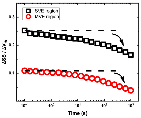
Figure 7.
drops with time in FinFET [29].
2.3.2. Trap-Based HCD Model
Taking the interface traps and oxide traps into consideration, a multitrap-based model is proposed and can decompose the contribution of different traps to HCD [29,31]. The total degradation can be modeled by the following equations [29]:
where is the saturation value of the interface trap, AR is the aging rate and is active energy. The model was tested using the following strategy: (1) extract the trap parameter in the single carrier event (SCE) region; (2) calculate the HCD in the multi carrier event (MCE) region using the parameter obtained from the last step. Taking nFinFET as an example, the first step and second step are shown in Figure 8a,b [29], respectively. The prediction is well fitted with experiment data, and parameters between different carrier transport mechanisms are the same, which indicates the model is unified across different regions.
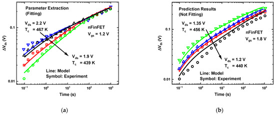
Figure 8.
(a) nFinFET experiment data (from Vds = 2.2 V to 1.9 V) used for parameter extraction in SCE region (Vd dependence); (b) comparison between model predictions by using parameters extracted from data in SCE region (line) and experiment data (from Vds = 1.35 V to 1.2 V) in MCE region (symbol) of nFinFET. The experiment data well agree with the prediction results [29].
2.4. Artificial Neural Network Model for HCI
Artificial neural networks are a powerful mathematical tool that can be used to solve complex problems as well as reduce simulation cost [75,76,77,78,79,80,81,82,83]. In order to reduce the simulation cost of numerical methods, an ANN model for 14 nm FinFET HCI prediction with consideration of the self-heating effect is proposed [33]. It can predict HCI induced TVS for FinFET under various environment temperatures and voltage stresses. The model has good accuracy and the average relative error is 0.36% [33]. Once the ANN model is built, it can greatly reduce simulation cost and has great potential in the reliability design of circuits and systems [33]. To train an accuracy ANN model, a large amount of experiment or simulation data are required.
2.4.1. Training Data
Simulation results produced using numerical methods introduced in Section 2.1 are used as the training data and divided into a test set (75%), training set (20%) and validation set (5%) [33]. The inputs are set as environment temperature and the features of stress including frequency, duty cycle, voltage amplitude and transition ratio. Min-Max normalization is applied to eliminate the impact of inconsistent data units,
where and are the data before and after normalization, respectively, and and are the minimum and maximum value in all x, respectively. The scaling parameter and normalized average temperature are set as the training targets. The diagram of the ANN model is shown in Figure 9 [33]. The optimizer is set to the Adam optimizer [84], and the loss function is the mean square error (MSE). The learning rate and the number of training epochs are set to 0.0005 and 100, respectively. The relative error of TVS under 10 years of stress voltage is applied to evaluate the accuracy of the model [33].
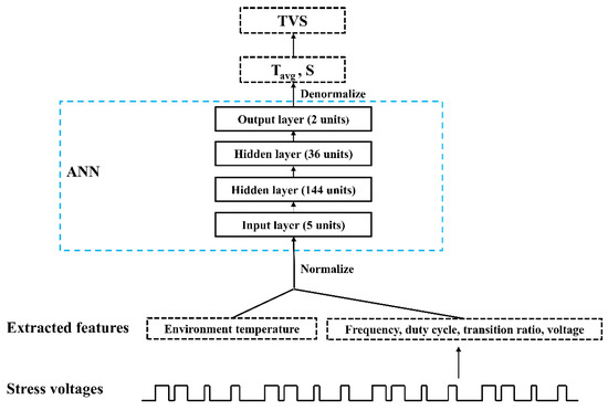
Figure 9.
Diagram of the ANN model [33].
2.4.2. Results
Figure 10 is the convergence graph of ANN training [33]. The errors in the validation set and test set are 0.37% and 0.36%, respectively, which means that even for unseen stress voltage conditions the network can predict TVS results accurately. Figure 11 shows the comparison of TVS predicted by ANN and experiments [42] under different (a) environment temperature, (b) voltage amplitude and (c) waveforms [33], in which the ANN results show good agreement with experiment results [33]. Figure 12 compares the ANN results and numerical simulation results under 10 years of stress voltage with different duty cycles, and the gap between the solid lines and dot lines is very small.
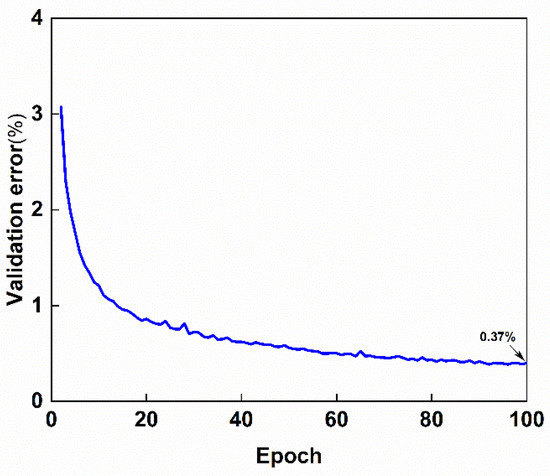
Figure 10.
Convergence graph of ANN training [33].
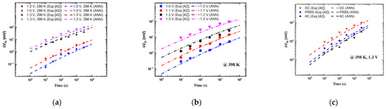
Figure 11.
The comparison between ANN results (dot line) and experiment data (symbol) [42]. (a) TVS under different environment temperatures; (b) TVS under stresses with different voltage amplitude; (c) TVS under stresses with different waveforms (DC, 5 GHz AC and 5 GHz PRBS) [33].
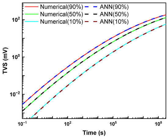
Figure 12.
The comparison between ANN results (dot line) and numerical simulation results (solid line) under 10 years of stress voltage with different duty cycles [33].
3. Conclusions
In summary, various models were developed to reveal the physical mechanisms behind the phenomena, and models were also built to predict the HCI induced device degradation. In this paper, numerical methods, analytical HCI model, trap-based HCI model and ANN model for HCI are reviewed and discussed in detail.
In terms of future research trends, the self-heating effect becomes more severe in gate-all-around devices such as nanosheets and nanowires due to the low thermal conductivity, high power density and stacked topologies that make it difficult to dissipate heat. The HCI will continue to be a significant reliability issue in these devices. There are many potential possibilities. As the carrier transport process become more and more complex for shorter-channel devices, the trap-based compact model that considers the influence of traps is meaningful. Numerical methods are capable to solve TVS under diverse stress voltages with different waveforms and frequencies. However, the simulation cost is high. On the other hand, artificial neural networks are a powerful tool to solve complex problems and reduce simulation cost. Reliability design in circuits and systems with the aid of artificial intelligence is of great potential. It is also very helpful to explore powerful and accurate compact models to give a more complete description of the HCI in advanced nanoscale field effect transistors.
Author Contributions
W.C., Y.L. and Y.W. conceived of the presented idea. Y.W., Y.L., Y.Y. and W.C. performed the literature research and discussed the related results. All authors contributed to the final manuscript. All authors have read and agreed to the published version of the manuscript.
Funding
This research was funded by the National Natural Science Foundation of China (NSFC) under Grants No. 62122067 and 61971375, in part by the Zhejiang Provincial Natural Science Foundation under Grant No. LR21F010003, in part by National Key Laboratory Foundation HTKJ2021KL504017 and in part by Sichuan Science and Technology Program No. 2021YJ0087.
Institutional Review Board Statement
Not applicable.
Informed Consent Statement
Not applicable.
Data Availability Statement
Not applicable.
Conflicts of Interest
The authors declare no conflict of interest.
References
- Thewes, R.; Weber, W. Effects of Hot-Carrier Degradation in Analog Cmos Circuits. Microelectron. Eng. 1997, 36, 285–292. [Google Scholar] [CrossRef]
- Acovic, A.; La Rosa, G.; Sun, Y.-C. A Review of Hot-Carrier Degradation Mechanisms in Mosfets. Microelectron. Reliab. 1996, 36, 845–869. [Google Scholar] [CrossRef]
- Alam, M.A.; Mahajan, B.K.; Chen, Y.-P.; Ahn, W.; Jiang, H.; Shin, S.H. A Device-to-System Perspective Regarding Self-Heating Enhanced Hot Carrier Degradation in Modern Field-Effect Transistors: A Topical Review. IEEE Trans. Electron Devices 2019, 66, 4556–4565. [Google Scholar] [CrossRef]
- Reddy, V.; Martin, S.; Benaissa, K.; Chancellor, C.; Bhatia, K.; Srinivasan, V.; Rentala, V.; Krishnan, S.; Ondrusek, J. Challenges in Radio Frequency and Mixed-Signal Circuit Reliability. In Proceedings of the 2019 IEEE International Electron Devices Meeting (IEDM), San Francisco, CA, USA, 7–11 December 2019. [Google Scholar]
- Leblebici, Y. Design Considerations for Cmos Digital Circuits with Improved Hot-Carrier Reliability. IEEE J. Solid-State Circuits 1996, 31, 1014–1024. [Google Scholar] [CrossRef]
- Gupta, A.; Gupta, C.; Jatana, H.; Dixit, A. Investigation of Hot-Carrier Degradation in 0.18-μ M Mosfets for the Evaluation of Device Lifetime and Digital Circuit Performance. IEEE Trans. Device Mater. Reliab. 2019, 19, 609–614. [Google Scholar] [CrossRef]
- Hu, C.; Tam, S.C.; Hsu, F.-C.; Ko, P.-K.; Chan, T.-Y.; Terrill, K.W. Hot-Electron-Induced Mosfet Degradation-Model, Monitor, and Improvement. IEEE J. Solid-State Circuits 1985, 20, 295–305. [Google Scholar]
- McMahon, W.; Hess, K. A Multi-Carrier Model for Interface Trap Generation. J. Comput. Electron. 2002, 1, 395–398. [Google Scholar] [CrossRef]
- Guérin, C.; Huard, V.; Bravaix, A. General Framework about Defect Creation at the Si/SiO2 Interface. J. Appl. Phys. 2009, 105, 114513. [Google Scholar] [CrossRef]
- Tyaginov, S.; Grasser, T. Modeling of Hot-Carrier Degradation: Physics and Controversial Issues. In Proceedings of the 2012 IEEE International Integrated Reliability Workshop Final Report, South Lake Tahoe, CA, USA, 14–18 October 2012. [Google Scholar]
- Randriamihaja, Y.M.; Huard, V.; Federspiel, X.; Zaka, A.; Palestri, P.; Rideau, D.; Roy, D.; Bravaix, A. Microscopic Scale Characterization and Modeling of Transistor Degradation under Hc Stress. Microelectron. Reliab. 2012, 52, 2513–2520. [Google Scholar] [CrossRef]
- Tyaginov, S.; Jech, M.; Franco, J.; Sharma, P.; Kaczer, B.; Grasser, T. Understanding and Modeling the Temperature Behavior of Hot-Carrier Degradation in Sion Nmosfets. IEEE Electron Device Lett. 2015, 37, 84–87. [Google Scholar] [CrossRef]
- Ng, K.; Taylor, G. Effects of Hot-Carrier Trapping in N-and P-Channel Mosfet’s. IEEE Trans. Electron Devices 1983, 30, 871–876. [Google Scholar] [CrossRef]
- Brunet, L.; Garros, X.; Bravaix, A.; Subirats, A.; Andrieu, F.; Weber, O.; Scheiblin, P.; Rafik, M.; Vincent, E.; Reimbold, G. Impact of Backside Interface on Hot Carriers Degradation of Thin Film Fdsoi Nmosfets. In Proceedings of the 2012 IEEE International Reliability Physics Symposium (IRPS), Anaheim, CA, USA, 15–19 April 2012. [Google Scholar]
- Kim, Y.; Kang, S.C.; Lee, S.K.; Jung, U.; Kim, S.M.; Lee, B.H. Hot-Carrier Instability of Nmosfets under Pseudorandom Bit Sequence Stress. IEEE Electron Device Lett. 2016, 37, 366–368. [Google Scholar] [CrossRef]
- Gupta, A.; Gupta, C.; Vega, R.A.; Hook, T.B.; Dixit, A. Reliability Modeling and Analysis of Hot-Carrier Degradation in Multiple-Fin Soi N-Channel Finfets with Self-Heating. IEEE Trans. Electron Devices 2019, 66, 2075–2080. [Google Scholar] [CrossRef]
- Mahapatra, S.; Sharma, U. A Review of Hot Carrier Degradation in N-Channel Mosfets—Part I: Physical Mechanism. IEEE Trans. Electron Devices 2020, 67, 2660–2671. [Google Scholar] [CrossRef]
- Ayala, N.; Martin-Martinez, J.; Amat, E.; Gonzalez, M.B.; Verheyen, P.; Rodriguez, R.; Nafria, M.; Aymerich, X.; Simoen, E. Nbti Related Time-Dependent Variability of Mobility and Threshold Voltage in Pmosfets and Their Impact on Circuit Performance. Microelectron. Eng. 2011, 88, 1384–1387. [Google Scholar] [CrossRef]
- Lorenz, D.; Georgakos, G.; Schlichtmann, U. Aging Analysis of Circuit Timing Considering Nbti and Hci. In Proceedings of the 2009 15th IEEE International On-Line Testing Symposium, Lisbon, Portugal, 24–26 June 2009. [Google Scholar]
- Fang, J.; Sapatnekar, S.S. Incorporating Hot-Carrier Injection Effects into Timing Analysis for Large Circuits. IEEE Trans. Very Large Scale Integr. Syst. 2014, 22, 2738–2751. [Google Scholar] [CrossRef]
- Wang, H.H.; Shieh, P.S.; Huang, C.T.; Tokami, K.; Kuo, R.; Chen, S.H.; Wei, H.C.; Pittikoun, S.; Aritome, S. A New Read-Disturb Failure Mechanism Caused by Boosting Hot-Carrier Injection Effect in Mlc Nand Flash Memory. In Proceedings of the 2009 IEEE International Memory Workshop, Monterey, CA, USA, 10–14 May 2009. [Google Scholar]
- Pouyan, P.; Amat, E.; Rubio, A. Reliability Challenges in Design of Memristive Memories. In Proceedings of the 2014 5th European Workshop on CMOS Variability (VARI), Palma de Mallorca, Spain, 29 September–1 October 2014. [Google Scholar]
- Goo, J.-S.; Kim, Y.-G.; L’Yee, H.; Kwon, H.-Y.; Shin, H. An Analytical Model for Hot-Carrier-Induced Degradation of Deep-Submicron N-Channel Ldd Mosfets. Solid-State Electron. 1995, 38, 1191–1196. [Google Scholar] [CrossRef]
- Rauch, S.E.; La Rosa, G. The Energy-Driven Paradigm of Nmosfet Hot-Carrier Effects. IEEE Trans. Device Mater. Reliab. 2005, 5, 701–705. [Google Scholar] [CrossRef]
- Bina, M.; Tyaginov, S.; Franco, J.; Rupp, K.; Wimmer, Y.; Osintsev, D.; Kaczer, B.; Grasser, T. Predictive Hot-Carrier Modeling of N-Channel Mosfets. IEEE Trans. Electron Devices 2014, 61, 3103–3110. [Google Scholar] [CrossRef]
- Chen, W.; Cheng, R.; Wang, D.-W.; Song, H.; Wang, X.; Chen, H.; Li, E.; Yin, W.-Y.; Zhao, Y. Electrothermal Effects on Hot-Carrier Reliability in Soi Mosfets—Ac Versus Circuit-Speed Random Stress. IEEE Trans. Electron Devices 2016, 63, 3669–3676. [Google Scholar] [CrossRef]
- Zhang, P.; Chen, W.; Hu, J.; Yin, W.-Y. Electrothermal Effects on Hot Carrier Injection in N-Type Soi Finfet under Circuit-Speed Bias. IEEE Trans. Electron Devices 2017, 64, 3802–3807. [Google Scholar] [CrossRef]
- Jiang, H.; Shin, S.; Liu, X.; Zhang, X.; Alam, M.A. The Impact of Self-Heating on Hci Reliability in High-Performance Digital Circuits. IEEE Electron Device Lett. 2017, 38, 430–433. [Google Scholar] [CrossRef]
- Yu, Z.; Zhang, J.; Wang, R.; Guo, S.; Liu, C.; Huang, R. New Insights into the Hot Carrier Degradation (Hcd) in Finfet: New Observations, Unified Compact Model, and Impacts on Circuit Reliability. In Proceedings of the 2017 IEEE International Electron Devices Meeting (IEDM), San Francisco, CA, USA, 2–6 December 2017. [Google Scholar]
- Yu, Z.; Zhang, Z.; Sun, Z.; Wang, R.; Huang, R. On the Trap Locations in Bulk Finfets after Hot Carrier Degradation (Hcd). IEEE Trans. Electron Devices 2020, 67, 3005–3009. [Google Scholar] [CrossRef]
- Wang, R.; Sun, Z.; Liu, Y.Y.; Yu, Z.; Wang, Z.; Jiang, X.; Huang, R. Understanding Hot Carrier Reliability in Finfet Technology from Trap-Based Approach. In Proceedings of the 2021 IEEE International Electron Devices Meeting (IEDM), San Francisco, CA, USA, 11–16 December 2021. [Google Scholar]
- Sharma, U.; Mahapatra, S. A Spice Compatible Compact Model for Hot-Carrier Degradation in Mosfets under Different Experimental Conditions. IEEE Trans. Electron Devices 2018, 66, 839–846. [Google Scholar] [CrossRef]
- Wang, Y.; Li, E.; Duan, H.; Tian, L.; Zang, W.; Min, Q.; Chen, W. An Artificial Neural Network Model for Electro-Thermal Effect Affected Hot Carrier Injection Reliability in 14-Nm Finfets. IEEE Trans. Microw. Theory Tech. 2022, 1–8. [Google Scholar] [CrossRef]
- Ancona, M.G.; Saks, N.S.; McCarthy, D. Lateral Distribution of Hot-Carrier-Induced Interface Traps in Mosfets. IEEE Trans. Electron Devices 1988, 35, 2221–2228. [Google Scholar] [CrossRef]
- Amat, E.; Kauerauf, T.; Degraeve, R.; Rodríguez, R.; Nafría, M.; Aymerich, X.; Groeseneken, G. Channel Hot-Carrier Degradation in Pmos and Nmos Short Channel Transistors with High-K Dielectric Stack. Microelectron. Eng. 2010, 87, 47–50. [Google Scholar] [CrossRef]
- Wu, Q.; Bayerl, A.; Porti, M.; Martin-Martínez, J.; Lanza, M.; Rodriguez, R.; Velayudhan, V.; Nafria, M.; Aymerich, X.; Gonzalez, M.B.; et al. A Conductive Afm Nanoscale Analysis of Nbti and Channel Hot-Carrier Degradation in Mosfets. IEEE Trans. Electron Devices 2014, 61, 3118–3124. [Google Scholar] [CrossRef]
- Bayer, A.; Porti, M.; Martin-Martínez, J.; Lanza, M.; Rodriguez, R.; Velayudhan, V.; Amat, E.; Nafria, M.; Aymerich, X.; Gonzalez, M.B.; et al. Channel Hot-Carriers Degradation in Mosfets: A Conductive Afm Study at the Nanoscale. In Proceedings of the 2013 IEEE International Reliability Physics Symposium (IRPS), Monterey, CA, USA, 14–18 April 2013. [Google Scholar]
- Laurent, A.; Garros, X.; Barraud, S.; Mariniello, G.; Reimbold, G.; Roy, D.; Vincent, E.; Ghibaudo, G. Hot Carrier Degradation in Nanowire Transistors: Physical Mechanisms, Width Dependence and Impact of Self-Heating. In Proceedings of the 2016 IEEE Symposium on VLSI Technology, Honolulu, HI, USA, 14–16 June 2016. [Google Scholar]
- Vandemaele, M.; Kaczer, B.; Tyaginov, S.; Bury, E.; Chasin, A.; Franco, J.; Makarov, A.; Mertens, H.; Hellings, G.; Groeseneken, G. Simulation Comparison of Hot-Carrier Degradation in Nanowire, Nanosheet and Forksheet Fets. In Proceedings of the 2022 IEEE International Reliability Physics Symposium (IRPS), Dallas, TX, USA, 27–31 March 2022. [Google Scholar]
- Chasin, A.; Bury, E.; Kaczer, B.; Franco, J.; Roussel, P.; Ritzenthaler, R.; Mertens, H.; Horiguchi, N.; Linten, D.; Mocuta, A. Complete Degradation Mapping of Stacked Gate-All-around Si Nanowire Transistors Considering Both Intrinsic and Extrinsic Effects. In Proceedings of the 2017 IEEE International Electron Devices Meeting (IEDM), San Francisco, CA, USA, 2–6 December 2017. [Google Scholar]
- Cheng, R.; Yu, X.; Shen, L.; Yin, L.; Zhang, Y.; Zheng, Z.; Chen, B.; Liu, X.; Zhao, Y. Ultrafast Pulse Characterization of Hot Carrier Injection Effects on Ballistic Carrier Transport for Sub-100 Nm Mosfets. In Proceedings of the 2017 IEEE International Reliability Physics Symposium (IRPS), Monterey, CA, USA, 2–6 April 2017. [Google Scholar]
- Qu, Y.; Lin, X.; Li, J.; Cheng, R.; Yu, X.; Zheng, Z.; Lu, J.; Chen, B.; Zhao, Y. Ultra Fast (<1 Ns) Electrical Characterization of Self-Heating Effect and Its Impact on Hot Carrier Injection in 14nm Finfets. In Proceedings of the 2017 IEEE International Electron Devices Meeting (IEDM), San Francisco, CA, USA, 2–6 December 2017. [Google Scholar]
- Jiang, H.; Liu, X.; Xu, N.; He, Y.; Du, G.; Zhang, X. Investigation of Self-Heating Effect on Hot Carrier Degradation in Multiple-Fin Soi Finfets. IEEE Electron Device Lett. 2015, 36, 1258–1260. [Google Scholar] [CrossRef]
- Hsu, F.-C.; Chiu, K.-Y. Temperature Dependence of Hot-Electron-Induced Degradation in Mosfet’s. IEEE Electron Device Lett. 1984, 5, 148–150. [Google Scholar] [CrossRef]
- Heremans, P.; Van den Bosch, G.; Bellens, R.; Groeseneken, G.; Maes, H. Understanding of the Temperature Dependence of Channel Hot-Carrier Degradation in the Range 77 K to 300 K. In Proceedings of the International Technical Digest on Electron Devices Meeting, Washington, DC, USA, 3–6 December 1989. [Google Scholar]
- Acovic, A.; Dutoit, M.; Ilegems, M. A Study of the Increased Effects of Hot-Carrier Stress on Nmosfets at Low Temperature. IEEE Trans. Electron Devices 1989, 36, 2603. [Google Scholar] [CrossRef]
- Heremans, P.; Van Den Bosch, G.; Bellens, R.; Groeseneken, G.; Maes, H.E. Temperature Dependence of the Channel Hot-Carrier Degradation of N-Channel Mosfet’s. IEEE Trans. Electron Devices 1990, 37, 980–993. [Google Scholar] [CrossRef]
- Song, M.; MacWilliams, K.P.; Woo, J.C. Comparison of Nmos and Pmos Hot Carrier Effects from 300 to 77 K. IEEE Trans. Electron Devices 1997, 44, 268–276. [Google Scholar] [CrossRef]
- Guérin, C.; Huard, V.; Bravaix, A. The Energy-Driven Hot-Carrier Degradation Modes of Nmosfets. IEEE Trans. Device Mater. Reliab. 2007, 7, 225–235. [Google Scholar] [CrossRef]
- Bravaix, A.; Guérin, C.; Huard, V.; Roy, D.; Roux, J.-M.; Vincent, E. Hot-Carrier Acceleration Factors for Low Power Management in Dc-Ac Stressed 40 nm Nmos Node at High Temperature. In Proceedings of the 2009 IEEE International Reliability Physics Symposium, Montreal, QC, Canada, 26–30 April 2009. [Google Scholar]
- Aminzadeh, P.; Alavi, M.; Scharfetter, D. Temperature Dependence of Substrate Current and Hot Carrier-Induced Degradation at Low Drain Bias. In Proceedings of the 1998 Symposium on VLSI Technology Digest of Technical Papers (Cat. No. 98CH36216), Honolulu, HI, USA, 9–11 June 1998. [Google Scholar]
- Amat, E.; Kauerauf, T.; Degraeve, R.; Rodriguez, R.; Nafria, M.; Aymerich, X.; Groeseneken, G. Competing Degradation Mechanisms in Short-Channel Transistors under Channel Hot-Carrier Stress at Elevated Temperatures. IEEE Trans. Device Mater. Reliab. 2009, 9, 454–458. [Google Scholar] [CrossRef]
- Pop, E.; Sinha, S.; Goodson, K.E. Heat Generation and Transport in Nanometer-Scale Transistors. Proc. IEEE 2006, 94, 1587–1601. [Google Scholar] [CrossRef]
- Chaudhry, A.; Kumar, M.J. Controlling Short-Channel Effects in Deep-Submicron Soi Mosfets for Improved Reliability: A Review. IEEE Trans. Device Mater. Reliab. 2004, 4, 99–109. [Google Scholar] [CrossRef]
- Jurczak, M.; Collaert, N.; Veloso, A.; Hoffmann, T.; Biesemans, S. Review of Finfet Technology. In Proceedings of the 2009 IEEE International SOI Conference, Foster City, CA, USA, 5–8 October 2009. [Google Scholar]
- Mishra, P.; Muttreja, A.; Jha, N.K. Finfet Circuit Design. In Nanoelectronic Circuit Design; Springer: New York, NY, USA, 2011. [Google Scholar]
- Sinha, S.; Yeric, G.; Chandra, V.; Cline, B.; Cao, Y. Exploring Sub-20nm Finfet Design with Predictive Technology Models. In Proceedings of the DAC Design Automation Conference 2012, San Francisco, CA, USA, 3–7 June 2012. [Google Scholar]
- Liu, W.; Asheghi, M. Thermal Conductivity Measurements of Ultra-Thin Single Crystal Silicon Layers. J. Heat Transf. 2005, 128, 75–83. [Google Scholar] [CrossRef]
- Scholten, A.; Smit, G.; Pijper, R.; Tiemeijer, L.; Tuinhout, H.; Van der Steen, J.-L.; Mercha, A.; Braccioli, M.; Klaassen, D. Experimental Assessment of Self-Heating in Soi Finfets. In Proceedings of the 2009 IEEE International Electron Devices Meeting (IEDM), Baltimore, MD, USA, 7–9 December 2009. [Google Scholar]
- Liu, S.; Wang, J.; Lu, Y.; Huang, D.; Huang, C.; Hsieh, W.; Lee, J.; Tsai, Y.; Shih, J.; Lee, Y.-H. Self-Heating Effect in Finfets and Its Impact on Devices Reliability Characterization. In Proceedings of the 2014 IEEE International Reliability Physics Symposium, Waikoloa, HI, USA, 1–5 June 2014. [Google Scholar]
- Jang, D.; Bury, E.; Ritzenthaler, R.; Bardon, M.G.; Chiarella, T.; Miyaguchi, K.; Raghavan, P.; Mocuta, A.; Groeseneken, G.; Mercha, A. Self-Heating on Bulk Finfet from 14nm Down to 7nm Node. In Proceedings of the 2015 IEEE International Electron Devices Meeting (IEDM), Washington, DC, USA, 7–9 December 2015. [Google Scholar]
- Fiegna, C.; Yang, Y.; Sangiorgi, E.; O’Neill, A.G. Analysis of Self-Heating Effects in Ultrathin-Body Soi Mosfets by Device Simulation. IEEE Trans. Electron Devices 2007, 55, 233–244. [Google Scholar] [CrossRef]
- Jiang, H.; Shin, S.; Liu, X.; Zhang, X.; Alam, M.A. Characterization of Self-Heating Leads to Universal Scaling of Hci Degradation of Multi-Fin Soi Finfets. In Proceedings of the 2016 IEEE International Reliability Physics Symposium (IRPS), Pasadena, CA, USA, 17–21 April 2016. [Google Scholar]
- Chen, W.; Yin, W.-Y.; Li, E.; Cheng, M.; Guo, J. Electrothermal Investigation on Vertically Aligned Single-Walled Carbon Nanotube Contacted Phase-Change Memory Array for 3-D Ics. IEEE Trans. Electron Devices 2015, 62, 3258–3263. [Google Scholar] [CrossRef]
- Chen, W.; Guo, J. Performance Analysis of Carbon Nanotube Contacted Phase Change Memory by Finite Element Method. J. Appl. Phys. 2011, 110, 084315. [Google Scholar] [CrossRef]
- Kwon, Y.W.; Bang, H. The Finite Element Method Using Matlab; CRC Press: Boca Raton, FL, USA, 2018. [Google Scholar]
- Xu, C.; Kolluri, S.K.; Endo, K.; Banerjee, K. Analytical Thermal Model for Self-Heating in Advanced Finfet Devices with Implications for Design and Reliability. IEEE Trans. Comput.-Aided Des. Integr. Circuits Syst. 2013, 32, 1045–1058. [Google Scholar] [CrossRef]
- Sun, J.; Li, X.; Sun, Y.; Shi, Y. Impact of Geometry, Doping, Temperature, and Boundary Conductivity on Thermal Characteristics of 14-Nm Bulk and Soi Finfets. IEEE Trans. Device Mater. Reliab. 2020, 20, 119–127. [Google Scholar] [CrossRef]
- Venkateswarlu, S.; Sudarsanan, A.; Singh, S.G.; Nayak, K. Ambient Temperature-Induced Device Self-Heating Effects on Multi-Fin Si N-Finfet Performance. IEEE Trans. Electron Devices 2018, 65, 2721–2728. [Google Scholar] [CrossRef]
- Zhang, X.; Connelly, D.; Takeuchi, H.; Hytha, M.; Mears, R.J.; Liu, T.-J.K. Comparison of Soi Versus Bulk Finfet Technologies for 6t-Sram Voltage Scaling at the 7-/8-Nm Node. IEEE Trans. Electron Devices 2016, 64, 329–332. [Google Scholar] [CrossRef]
- Takeda, E.; Suzuki, N. An Empirical Model for Device Degradation Due to Hot-Carrier Injection. IEEE Electron Device Lett. 1983, 4, 111–113. [Google Scholar] [CrossRef]
- Yu, Z.; Wang, R.; Hao, P.; Guo, S.; Ren, P.; Huang, R. Non-Universal Temperature Dependence of Hot Carrier Degradation (Hcd) in Finfet: New Observations and Physical Understandings. In Proceedings of the 2018 IEEE 2nd Electron Devices Technology and Manufacturing Conference (EDTM), Kobe, Japan, 13–16 March 2018. [Google Scholar]
- Yu, Z.; Sun, Z.; Wang, R.; Zhang, J.; Huang, R. Hot Carrier Degradation-Induced Dynamic Variability in Finfets: Experiments and Modeling. IEEE Trans. Electron Devices 2020, 67, 1517–1522. [Google Scholar] [CrossRef]
- Yang, C.; Chen, S.; Tsai, Y.; Lu, R.; Lee, Y.-H. The Physical Mechanism Investigation between Hk/Il Gate Stack Breakdown and Time-Dependent Oxygen Vacancy Trap Generation in Finfet Devices. In Proceedings of the 2016 IEEE International Reliability Physics Symposium (IRPS), Pasadena, CA, USA, 17–21 April 2016. [Google Scholar]
- Chen, X.; Wei, Z.; Li, M.; Rocca, P. A Review of Deep Learning Approaches for Inverse Scattering Problems (Invited Review). Prog. Electromagn. Res. 2020, 167, 67–81. [Google Scholar] [CrossRef]
- Wang, F.; Devabhaktuni, V.K.; Xi, C.; Zhang, Q.J. Neural Network Structures and Training Algorithms for Rf and Microwave Applications. Int. J. RF Microw. Comput.-Aided Eng. 1999, 9, 216–240. [Google Scholar] [CrossRef]
- Zhang, Q.-J.; Gupta, K.C.; Devabhaktuni, V.K. Artificial Neural Networks for Rf and Microwave Design-from Theory to Practice. IEEE Trans. Microw. Theory Tech. 2003, 51, 1339–1350. [Google Scholar] [CrossRef]
- Gabr, A.M.; Featherston, C.; Zhang, C.; Bonfil, C.; Zhang, Q.-J.; Smy, T.J. Design and Optimization of Optical Passive Elements Using Artificial Neural Networks. J. Opt. Soc. Am. B 2019, 36, 999–1007. [Google Scholar] [CrossRef]
- Marinković, Z.; Crupi, G.; Caddemi, A.; Marković, V.; Schreurs, D.M.P. A Review on the Artificial Neural Network Applications for Small-Signal Modeling of Microwave Fets. Int. J. Numer. Model. Electron. Netw. Devices Fields 2020, 33, e2668. [Google Scholar] [CrossRef]
- Marinković, Z.; Crupi, G.; Schreurs, D.M.-P.; Caddemi, A.; Marković, V. Microwave Finfet Modeling Based on Artificial Neural Networks Including Lossy Silicon Substrate. Microelectron. Eng. 2011, 88, 3158–3163. [Google Scholar] [CrossRef]
- Marinković, Z.; Crupi, G.; Schreurs, D.M.-P.; Caddemi, A.; Marković, V. Artificial Neural Network Based Modeling of Finfet Forward Transmission Coefficient. In Proceedings of the 2011 10th International Conference on Telecommunication in Modern Satellite Cable and Broadcasting Services (TELSIKS), Nis, Serbia, 5–8 October 2011. [Google Scholar]
- Marinković, Z.; Crupi, G.; Schreurs, D.M.P.; Caddemi, A.; Marković, V. Multibias Neural Modeling of Fin Field-Effect Transistor Admittance Parameters. Microw. Opt. Technol. Lett. 2012, 54, 2082–2088. [Google Scholar] [CrossRef]
- Crupi, G.; Schreurs, D.M.-P.; Raskin, J.-P.; Caddemi, A. A Comprehensive Review on Microwave Finfet Modeling for Progressing Beyond the State of Art. Solid-State Electron. 2013, 80, 81–95. [Google Scholar] [CrossRef]
- Kingma, D.P.; Ba, J. Adam: A Method for Stochastic Optimization. arXiv 2014, arXiv:1412.6980. [Google Scholar]


Publisher’s Note: MDPI stays neutral with regard to jurisdictional claims in published maps and institutional affiliations. |
© 2022 by the authors. Licensee MDPI, Basel, Switzerland. This article is an open access article distributed under the terms and conditions of the Creative Commons Attribution (CC BY) license (https://creativecommons.org/licenses/by/4.0/).