
A High-Efficiency High-Power-Density SiC-Based Portable Charger for Electric Vehicles

 , , ,
, , ,
Abstract
:1. Introduction
- The portable charger does not need to be stored in the vehicle if the level-3 dc charging function is mainly used, e.g., at a parking place of retail shops or at the workplace [26]. This releases construction space, which can be used for additional battery capacity and thus extends the range of the EV. Furthermore, the portable charger does not have to comply with automotive standards (lifetime, vibration stress).
- By using the established dc charging interfaces, a specific charger per vehicle type and manufacturer is not necessary. Portable chargers from different manufacturers would be compatible with each other, resulting in lower costs due to economies of scale, less electronic waste, and simple replacement in case of a defect.
- The universal approach opens up further possibilities: sharing or temporarily lending a portable charger, mobile charging services, and using the portable charger as a charging station at home.
2. Portable Off-Board Charger Specification
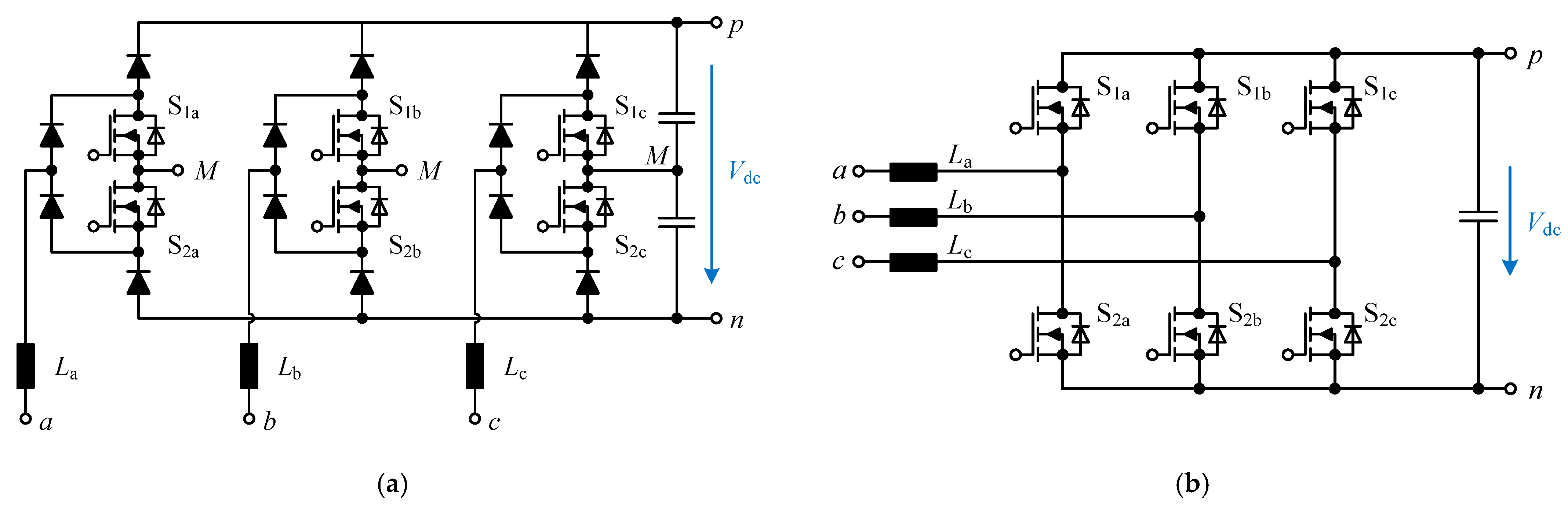
3. AC–DC Converter Stage
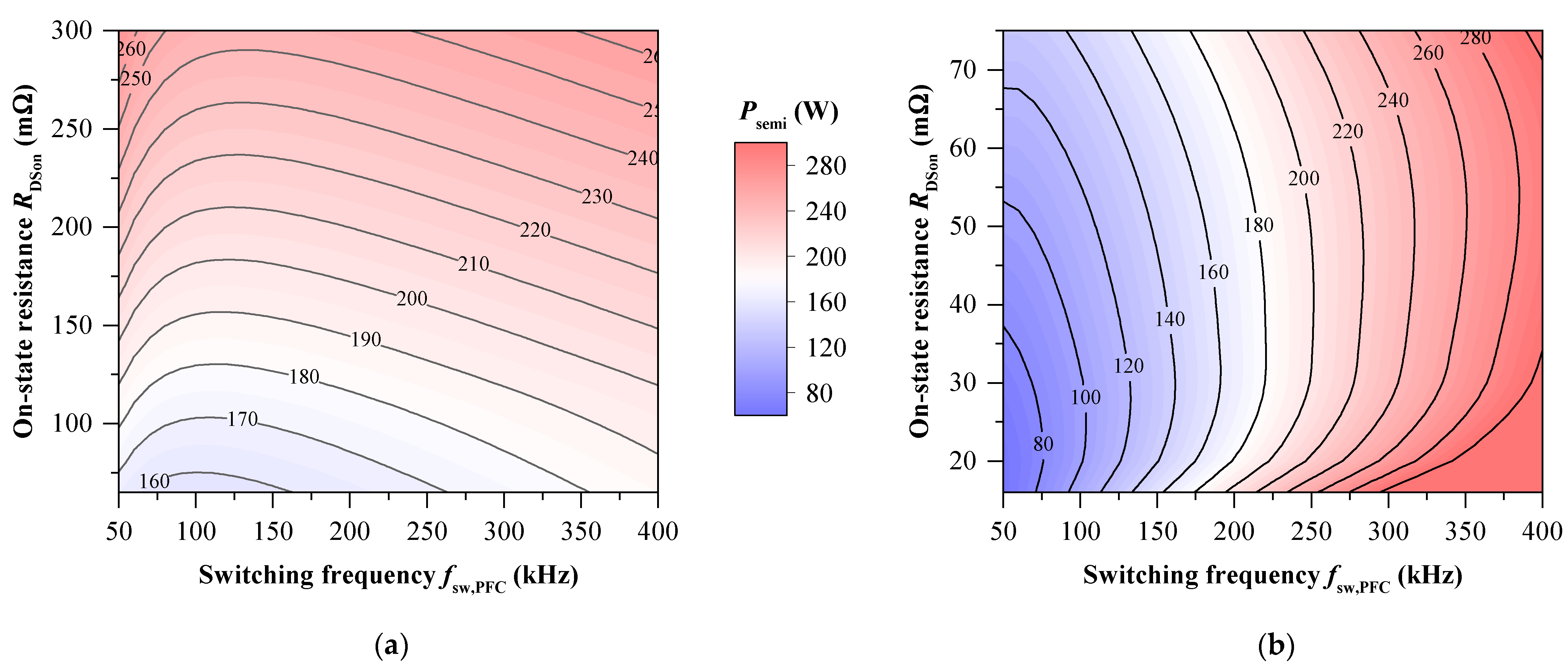
3.1. Evaluation of PFC Topology
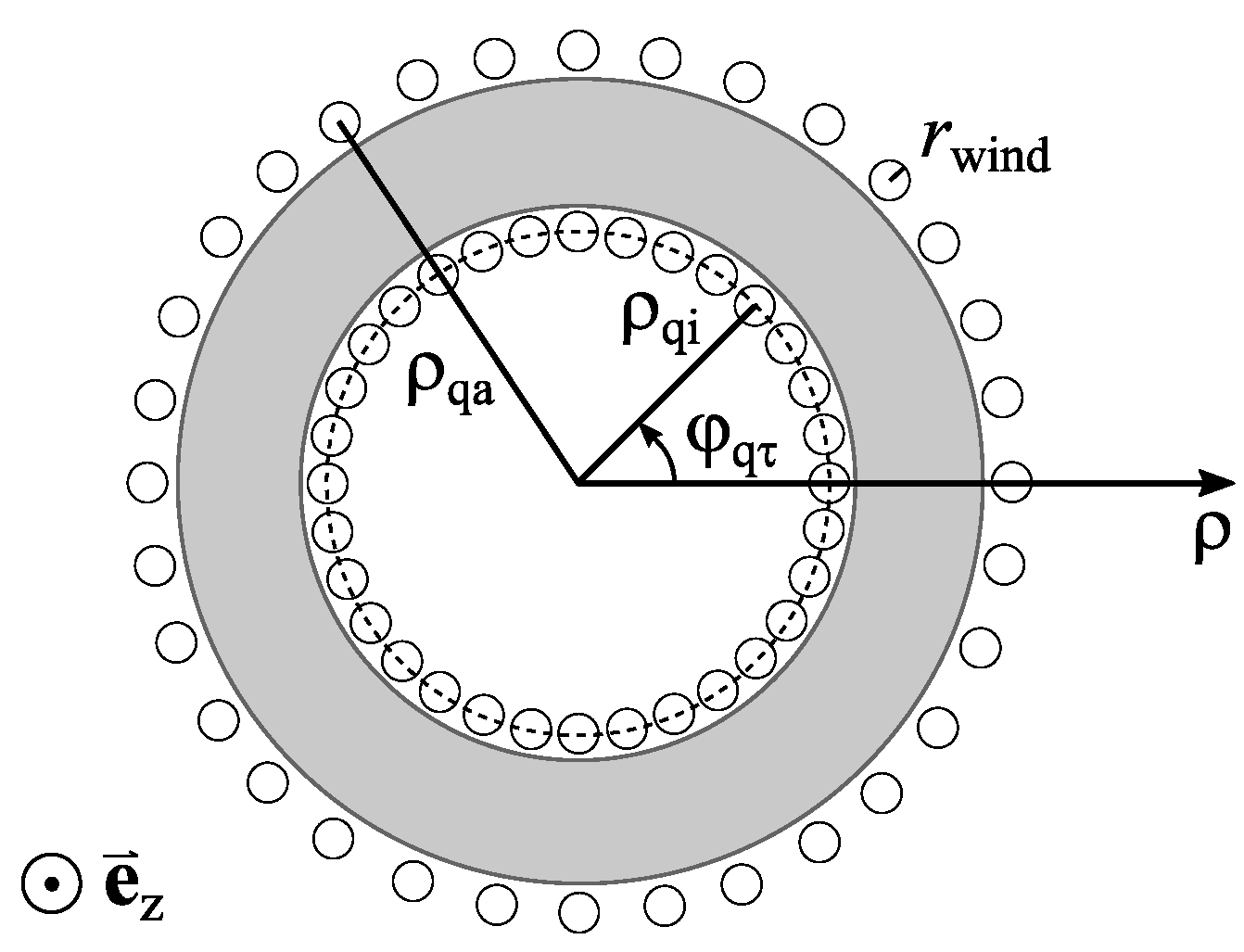
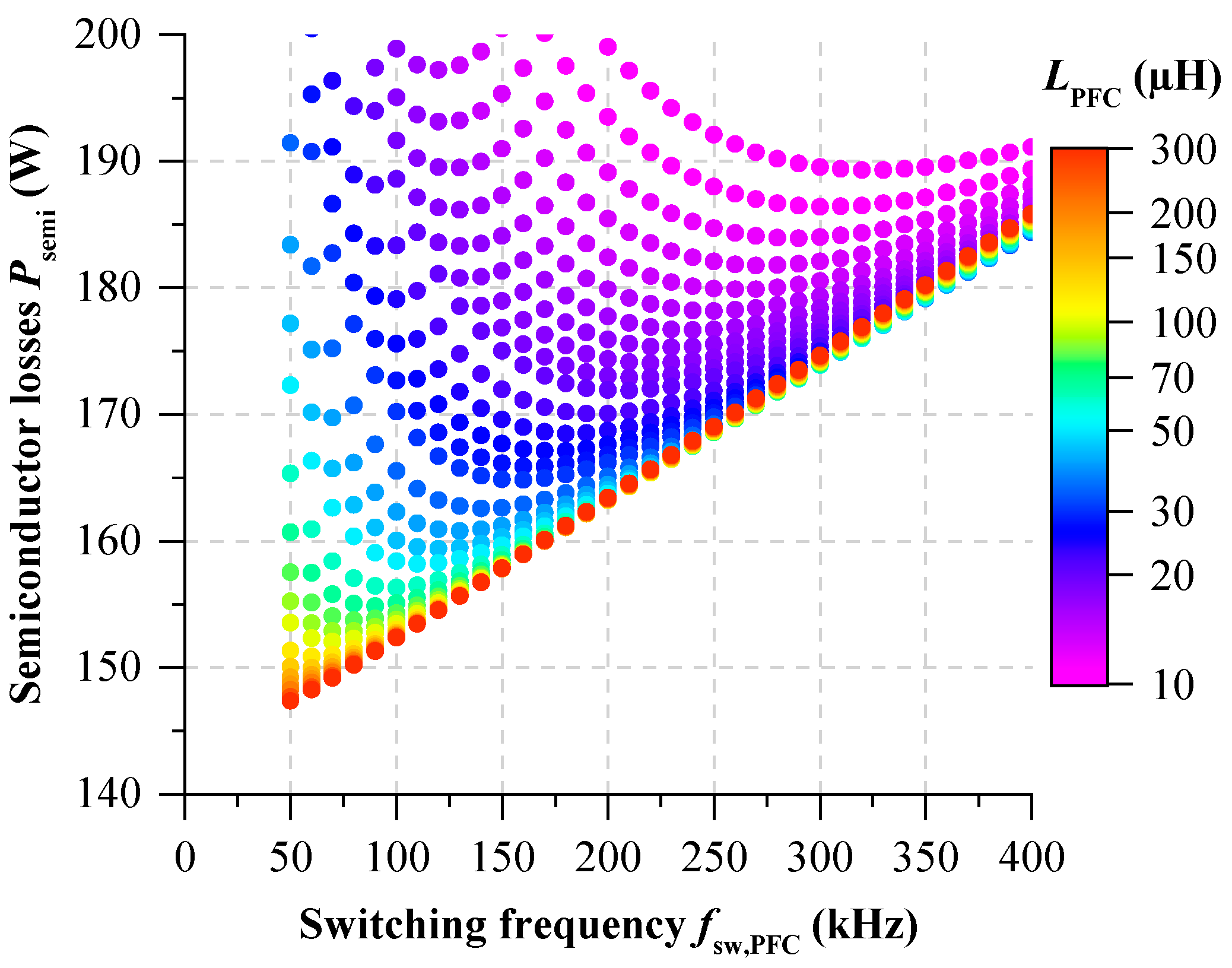
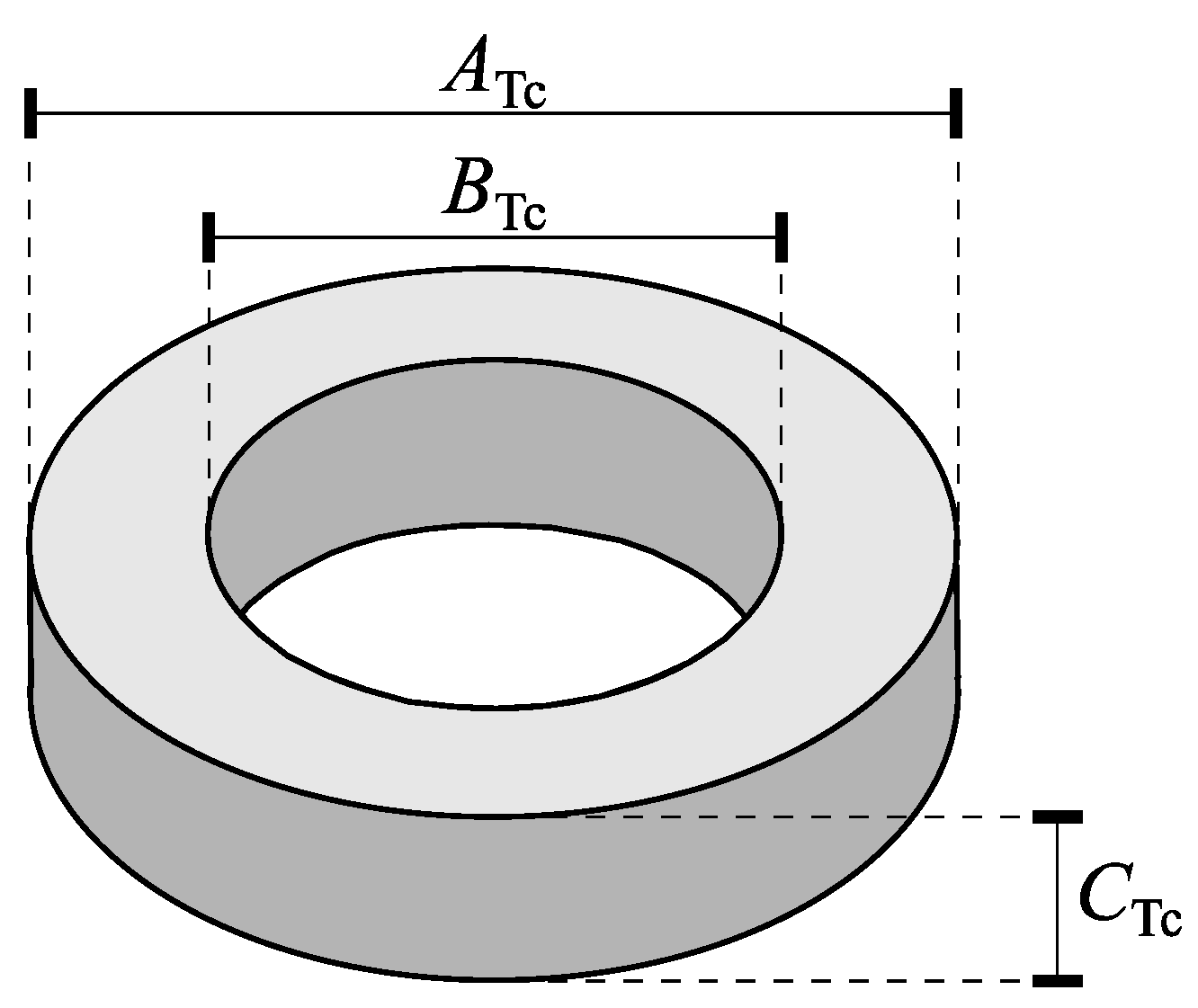
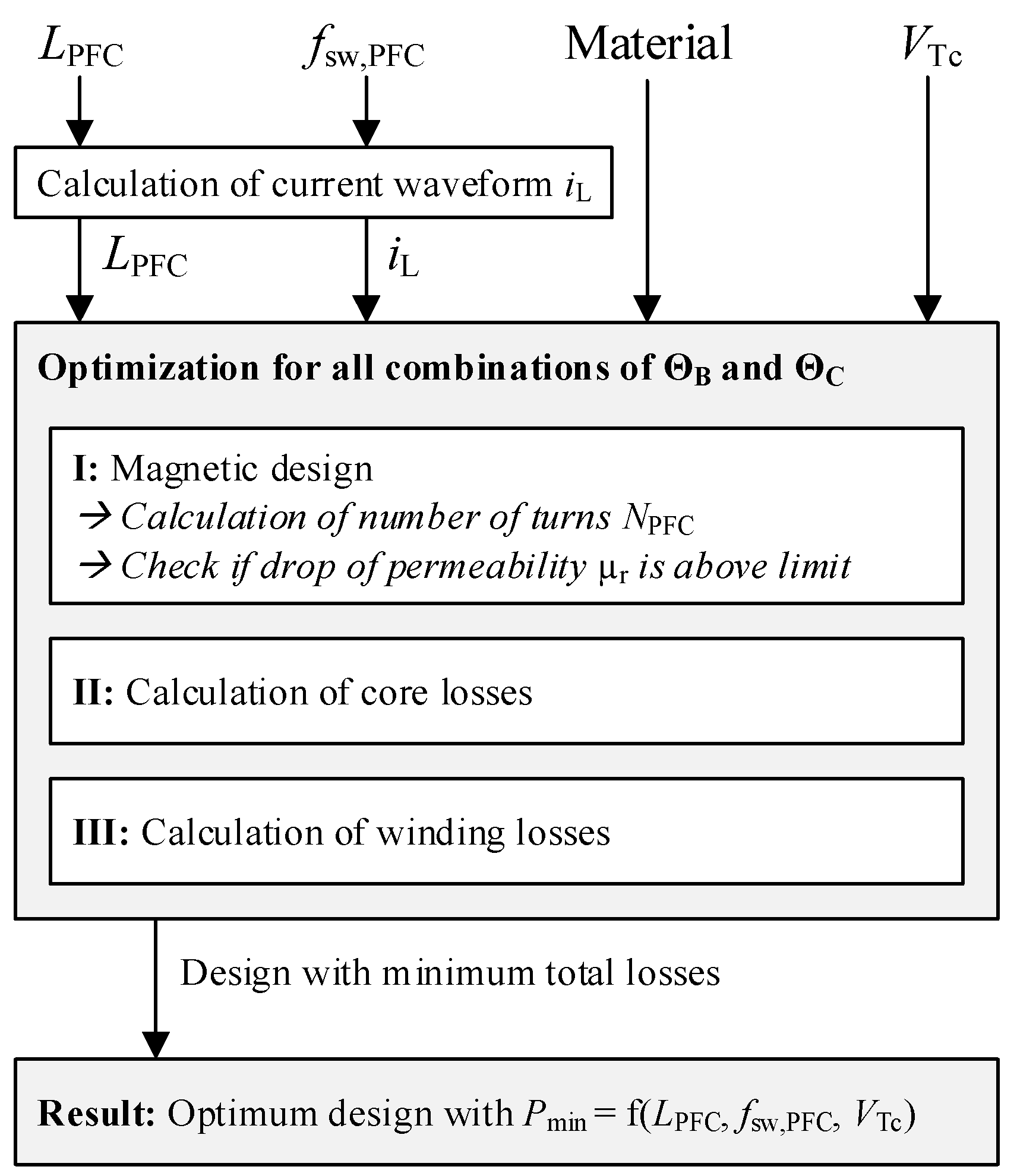
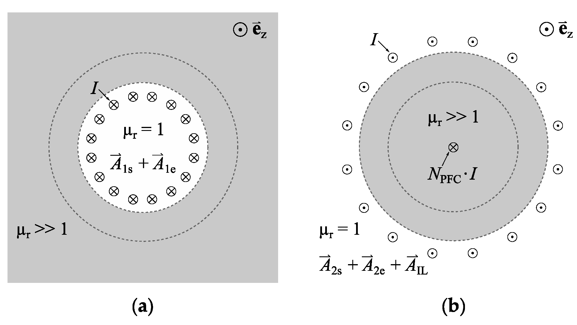
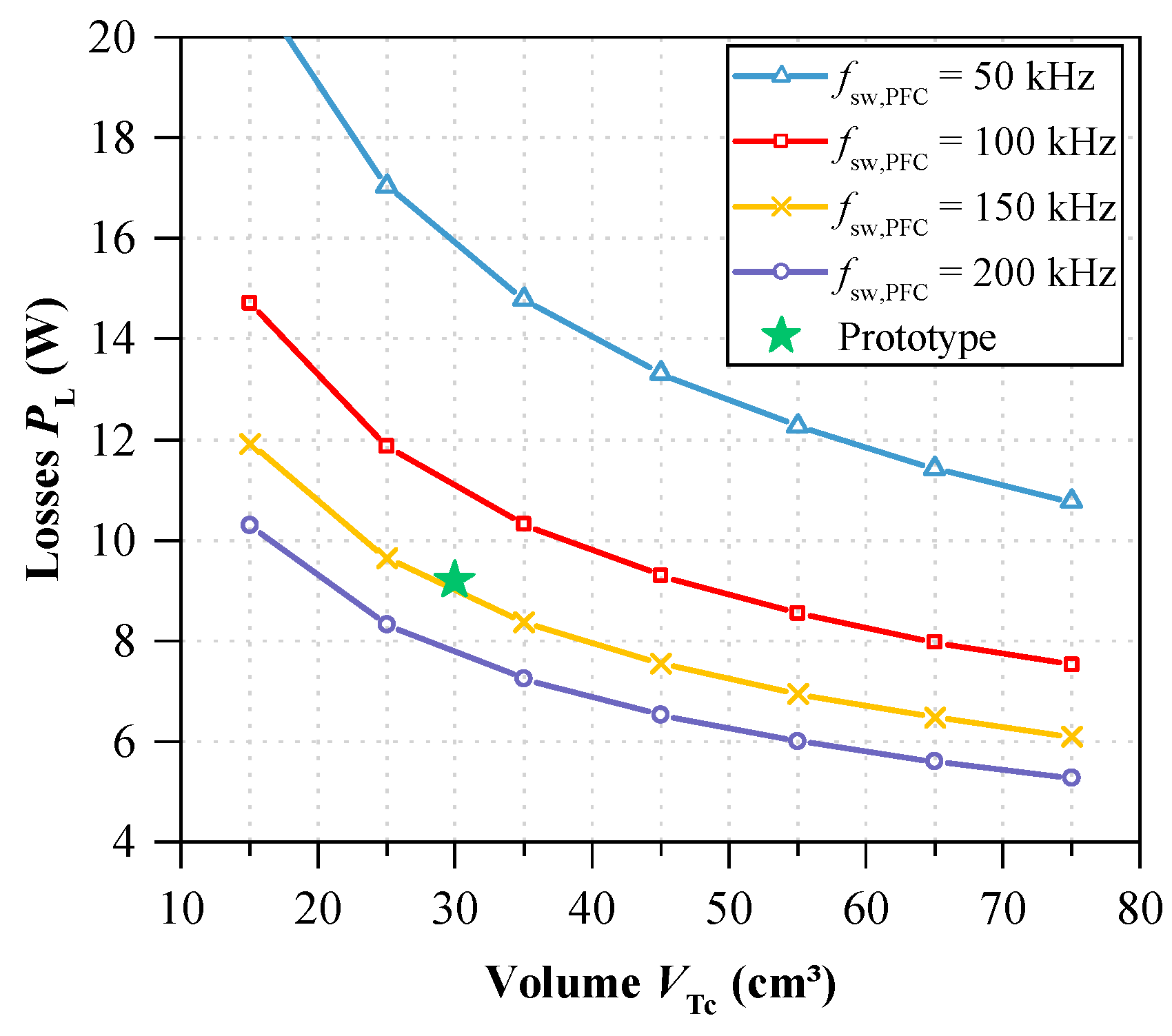
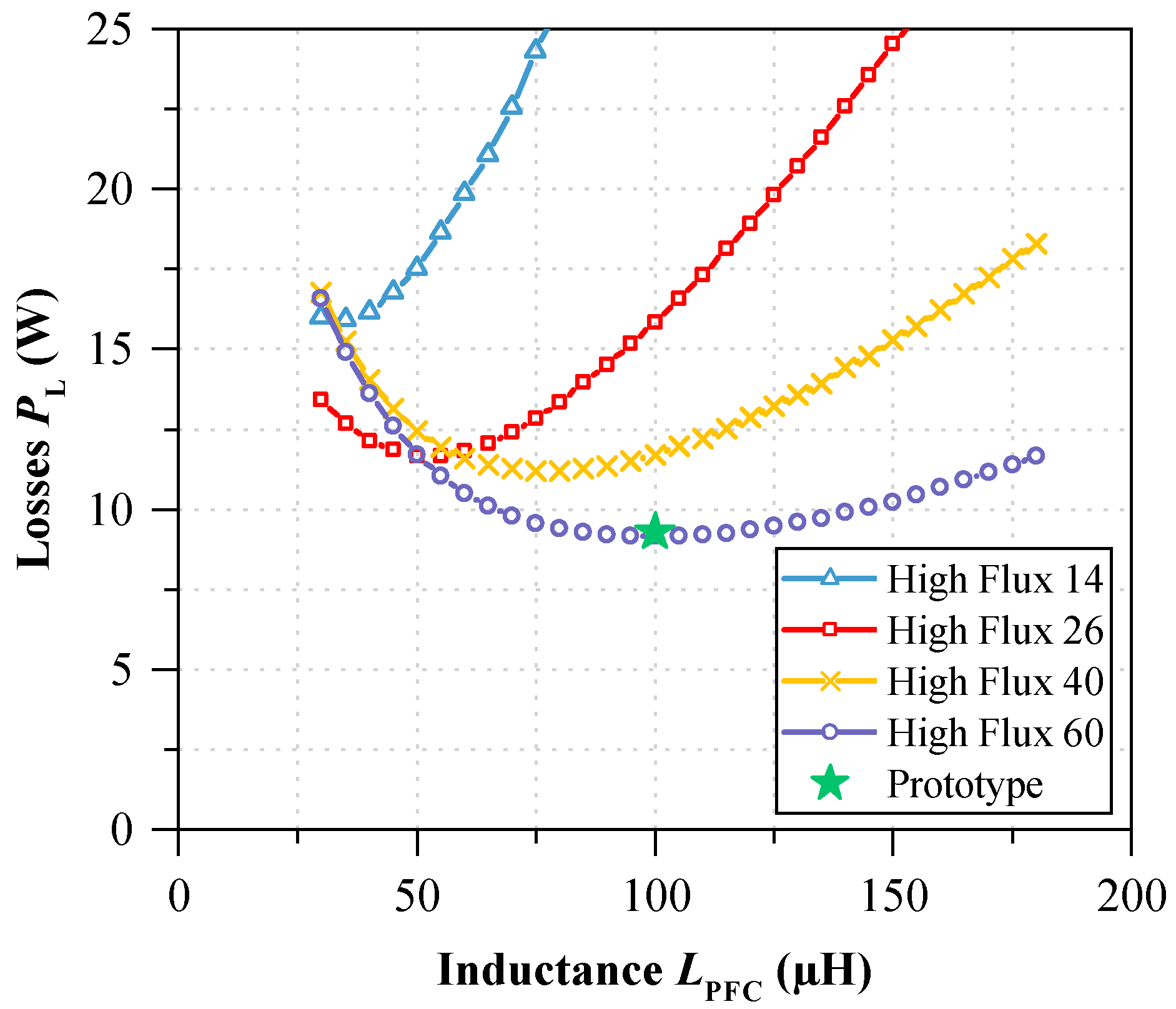
3.2. Inductor Design
4. DC-DC Converter Stage
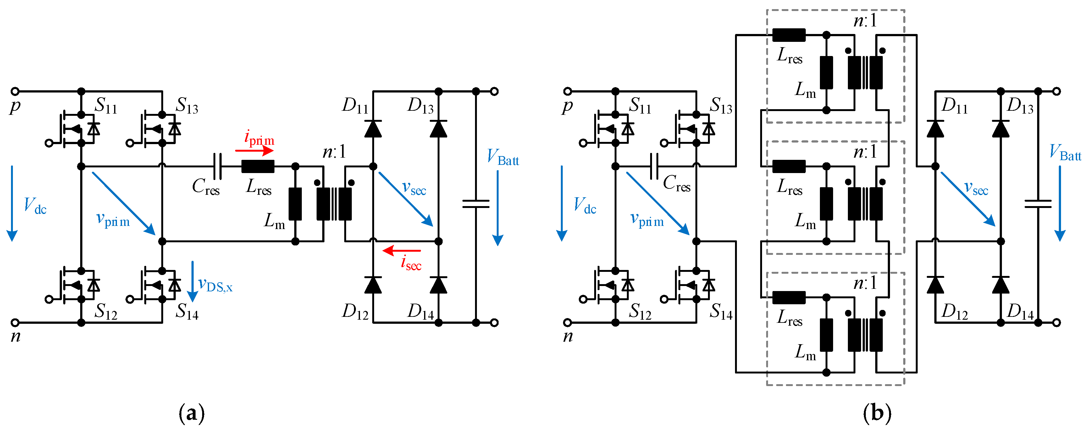
4.1. Configuration of the LLC Resonant Converter
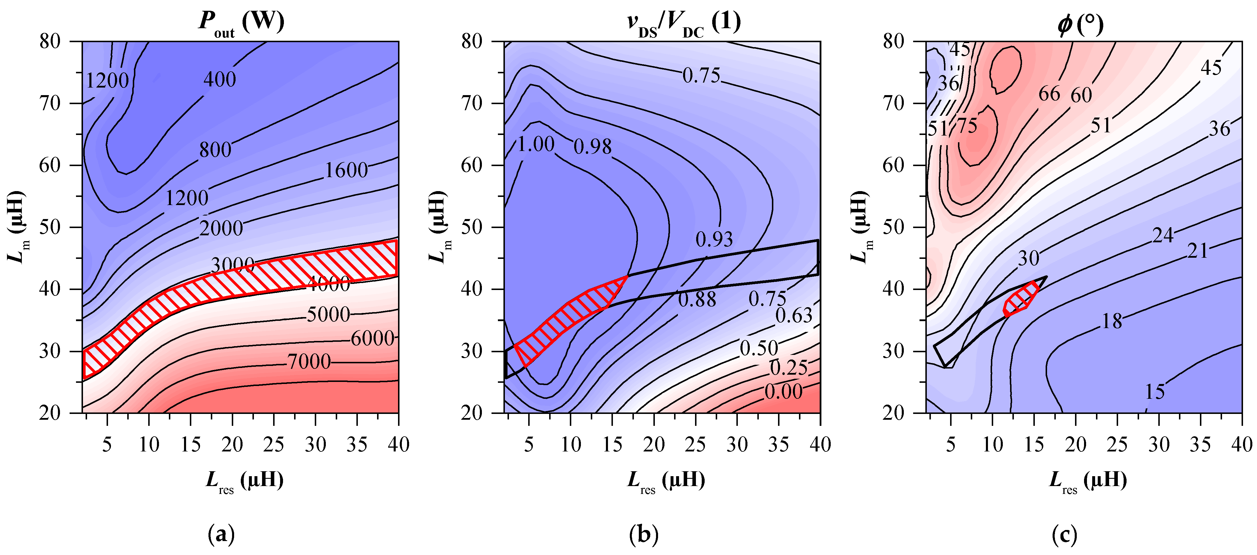
4.2. Design of the LLC Resonant Converter
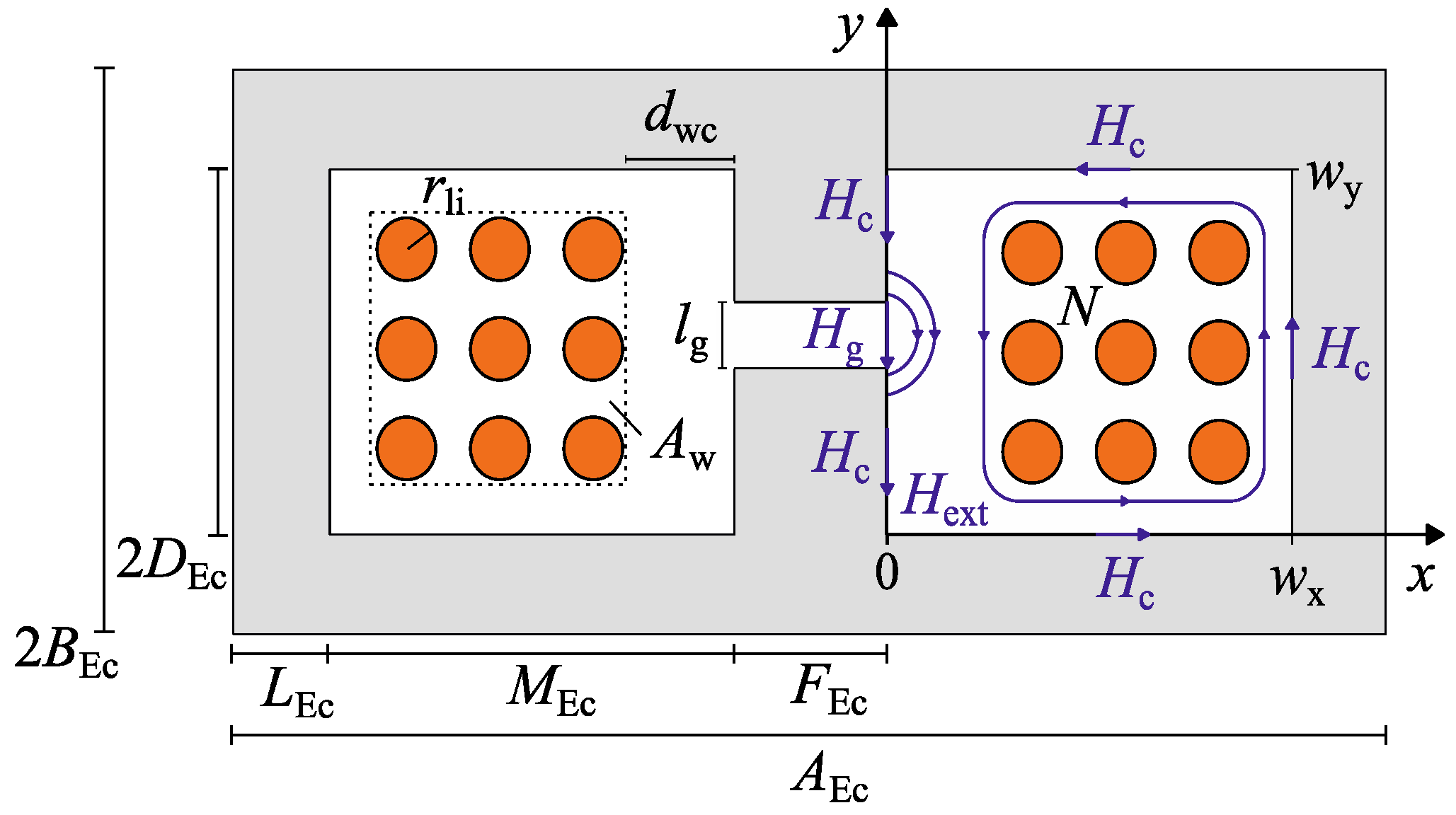
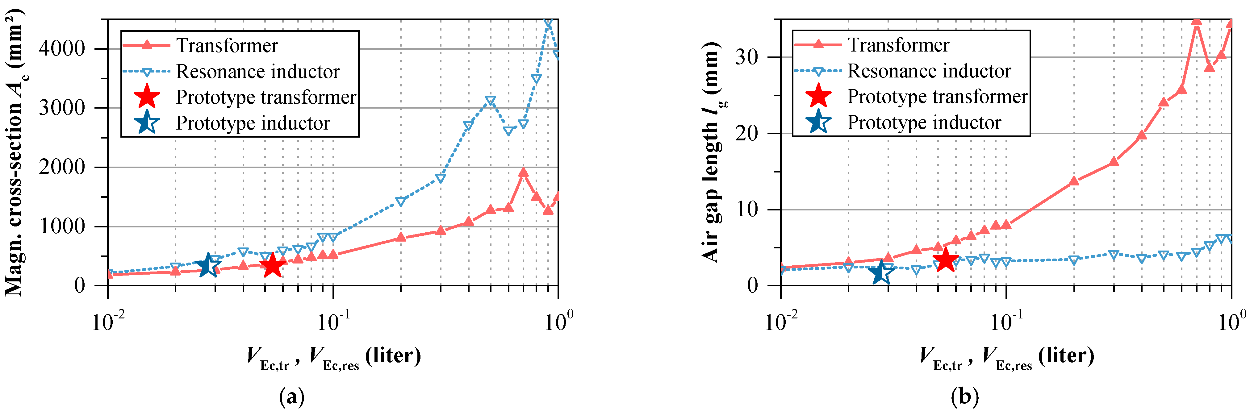
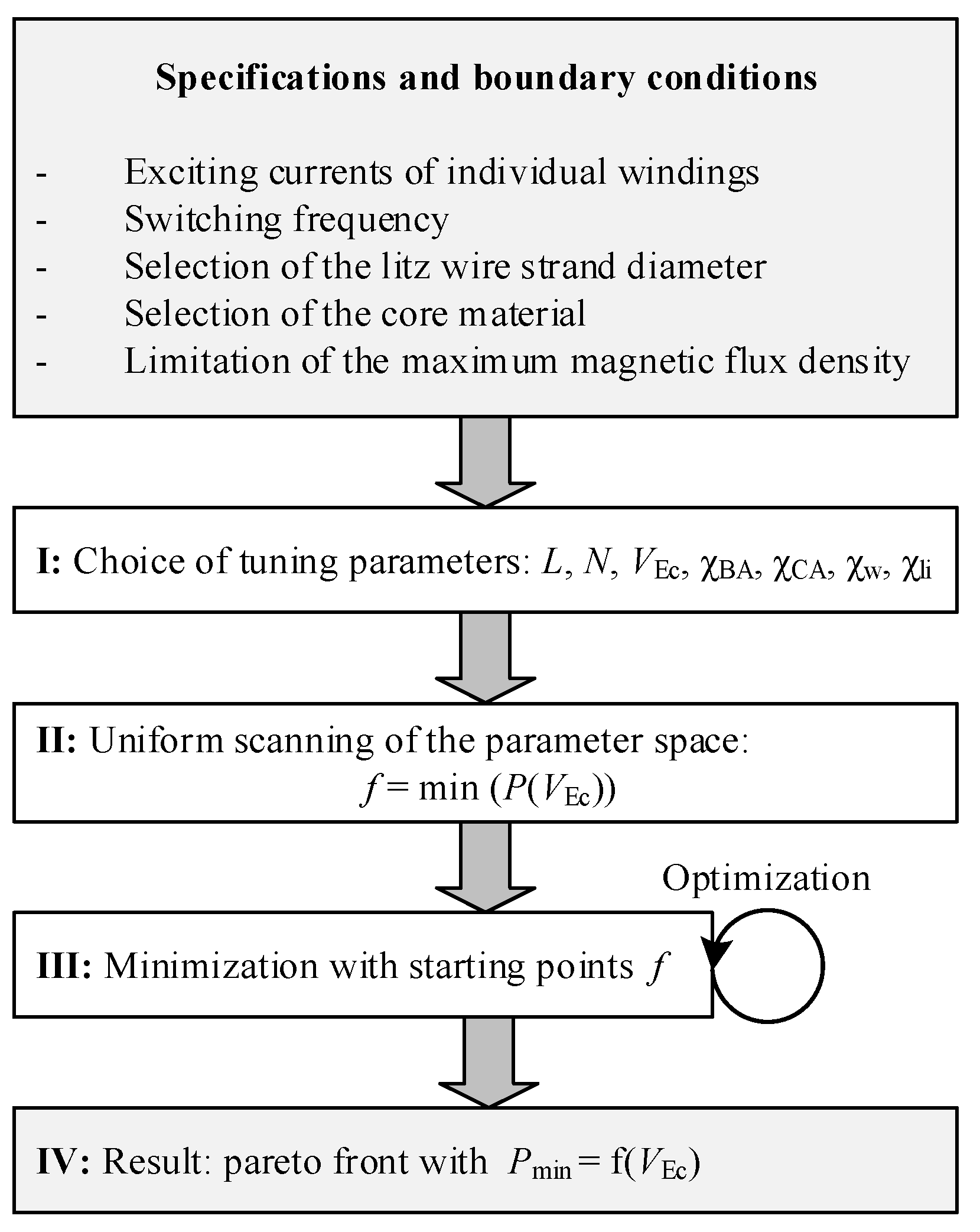
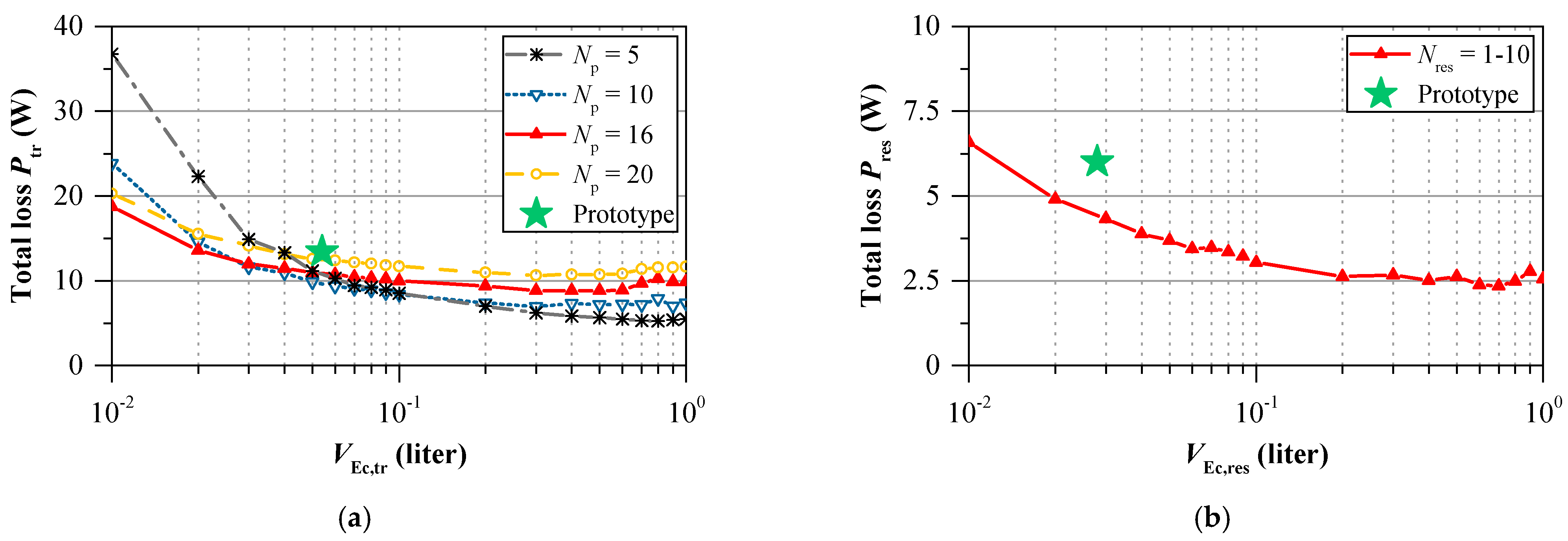
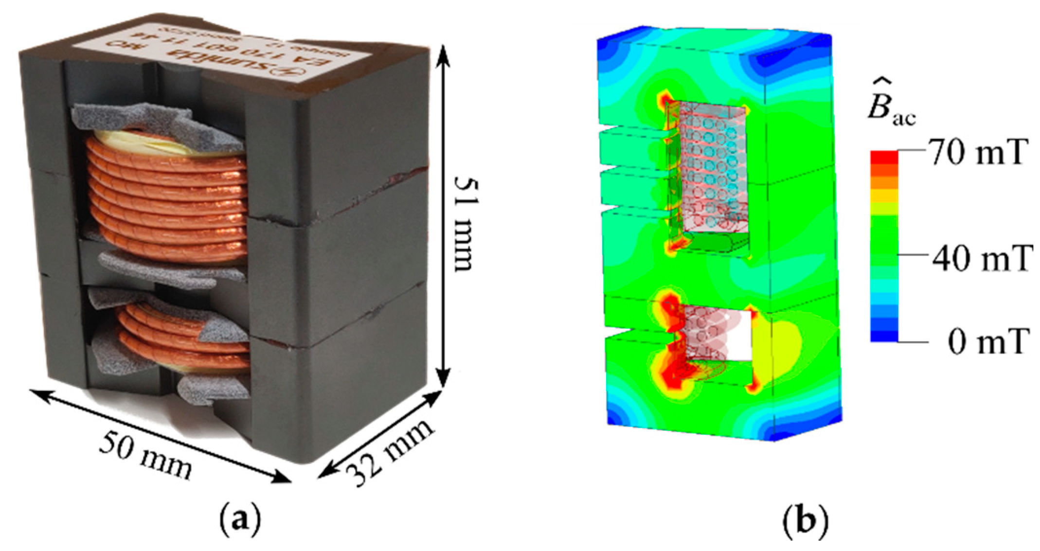
4.3. HF Transformer and Resonance Inductor Design
5. Control Strategy
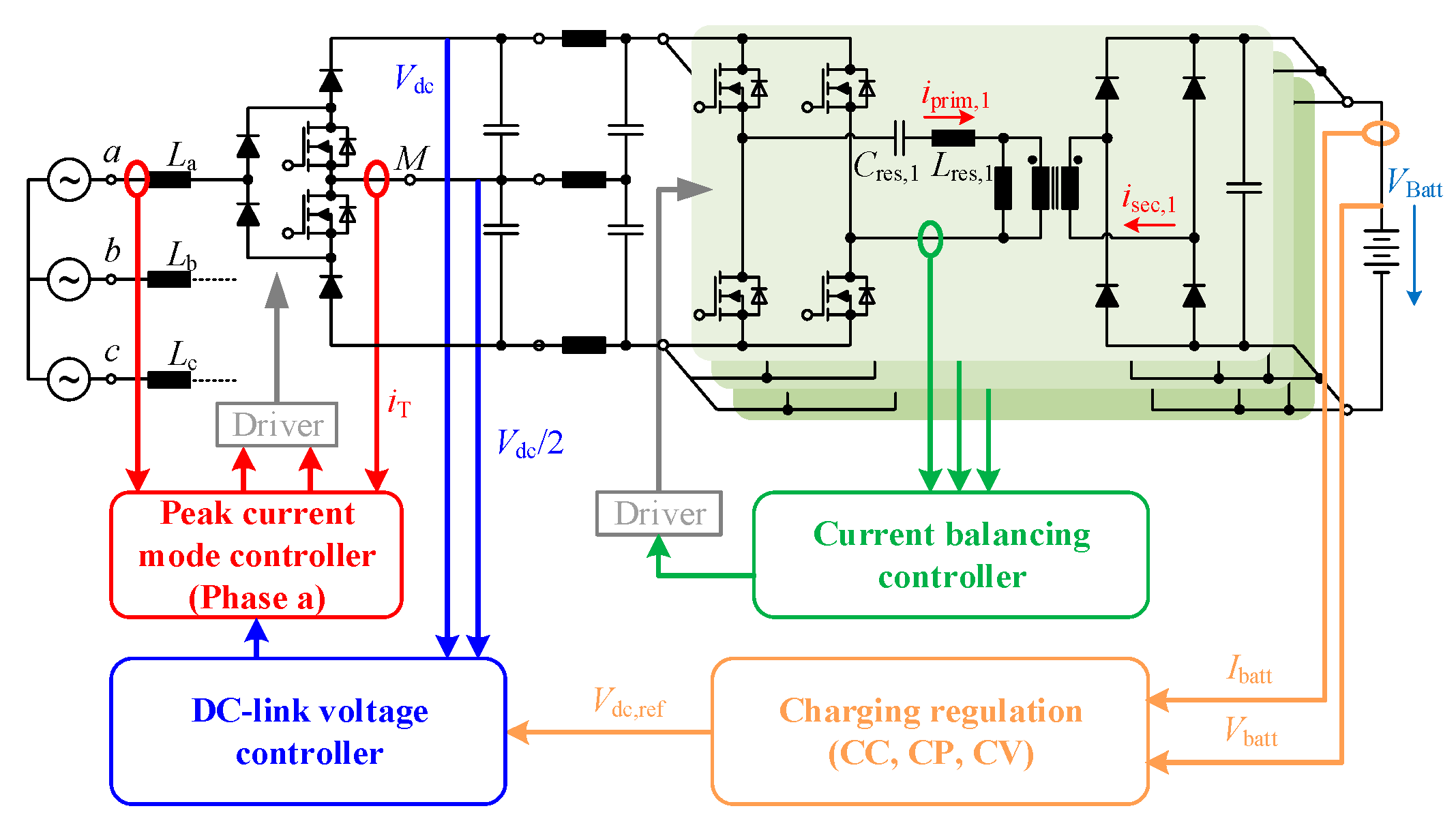
5.1. Two-Stage System Control
- The red control loop realizes the peak current mode control, the current limitation, and the PFC function. The current through the MOSFETs is sensed by a shunt, which is inserted between the MOSFETs and the “M” potential. A detailed description of the peak current mode control can be found in [69].
- The blue control loop is the outer voltage control loop for the dc-link, which also balances the voltage across the series-connected dc-link capacitors to ensure that they are uniformly loaded with Vdc/2 during operation. Only one voltage control loop is implemented, and the control value is passed to all three PFC current controllers.
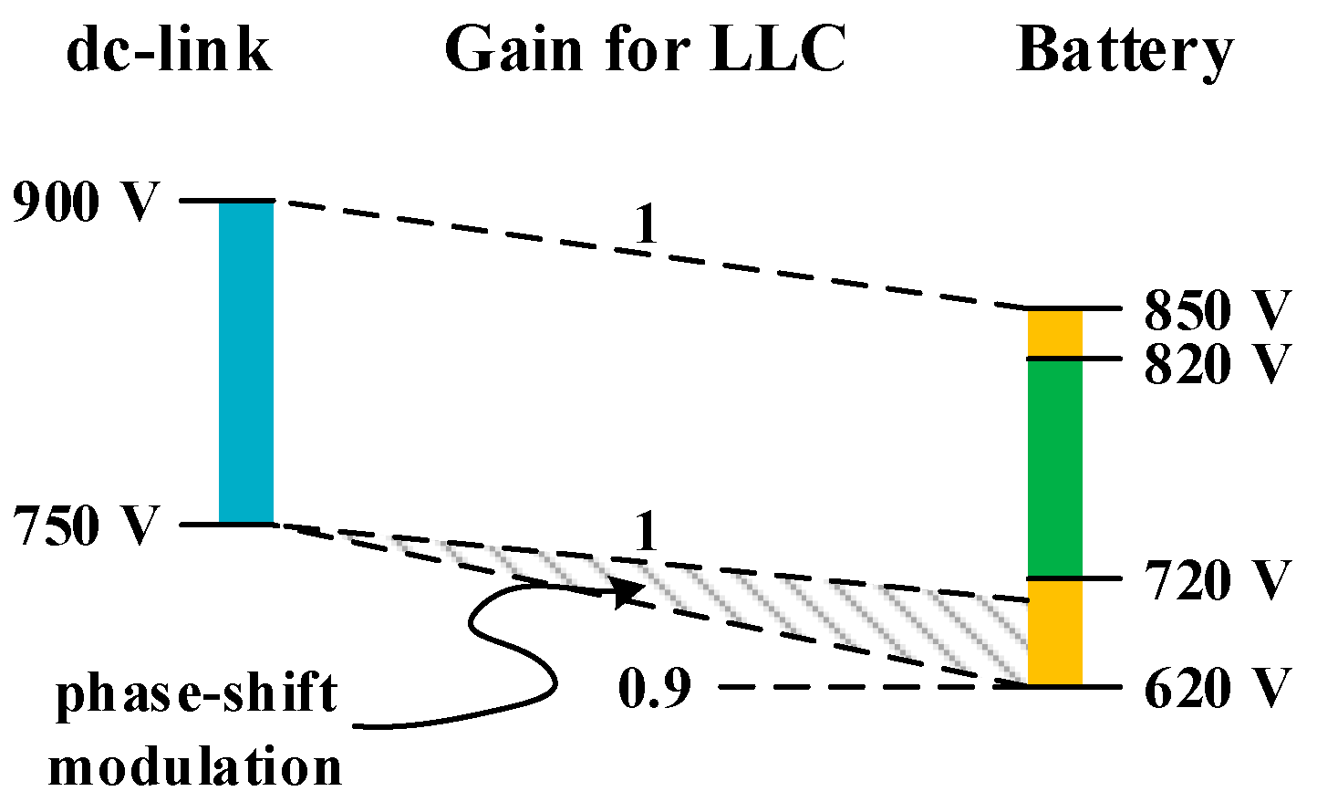
- A charge controller realizes the different charging modes “constant current” (CC), “constant power” (CP), and “constant voltage” (CV), which is shown in orange. A PI controller compares the measured output current multiplied by the battery voltage with the target output power. In addition, the current system temperatures are taken into account for the implementation of a derating function, which reduces the nominal value of the charging power depending on the thermal conditions. The control value of the charge controller is passed to the input of the blue voltage control loop and thus for the dc-link voltage, which is varied according to the current battery voltage and state of charge, respectively.
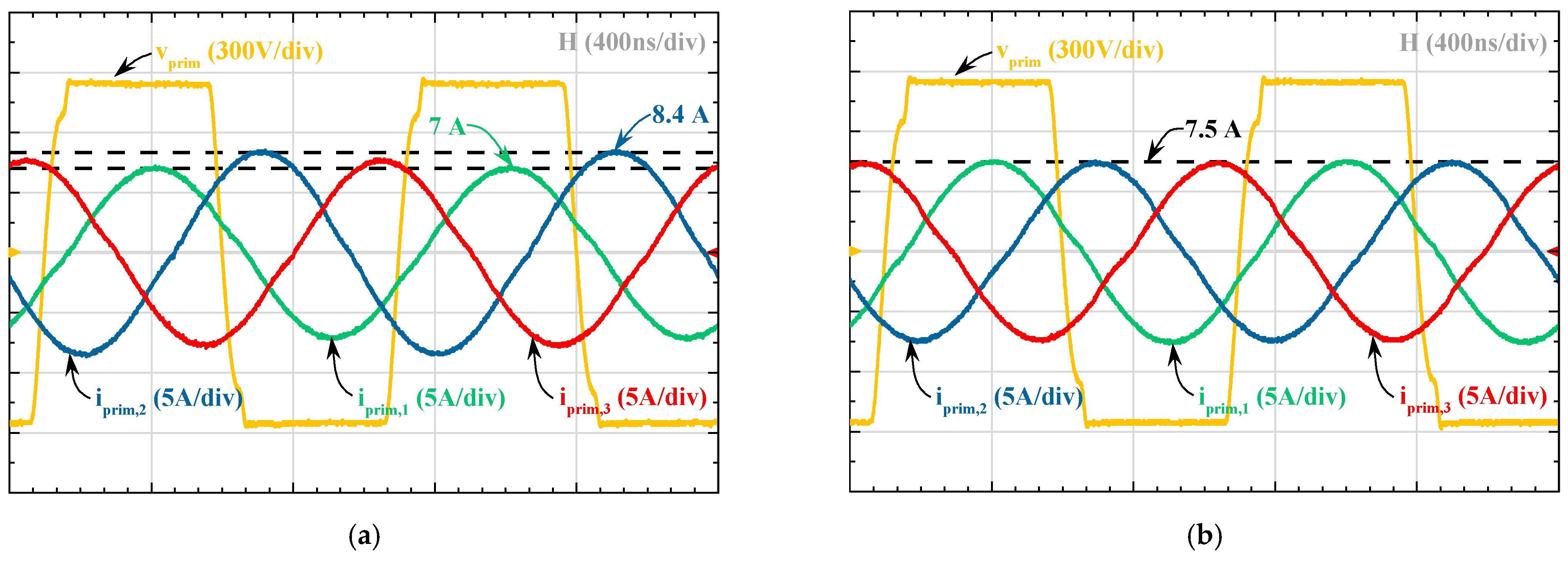
5.2. Current Sharing in LLC Resonant Converter
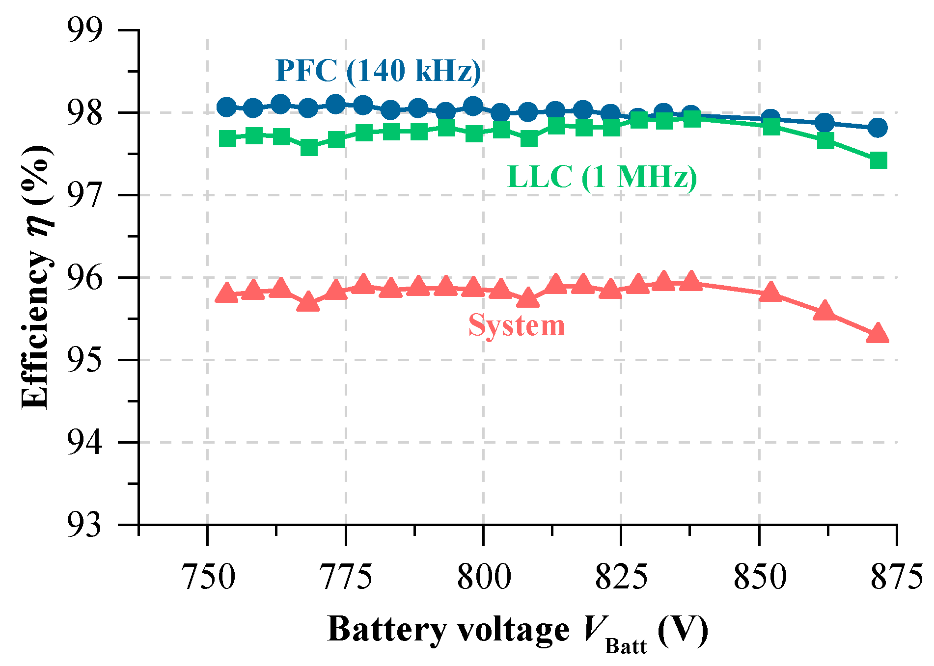
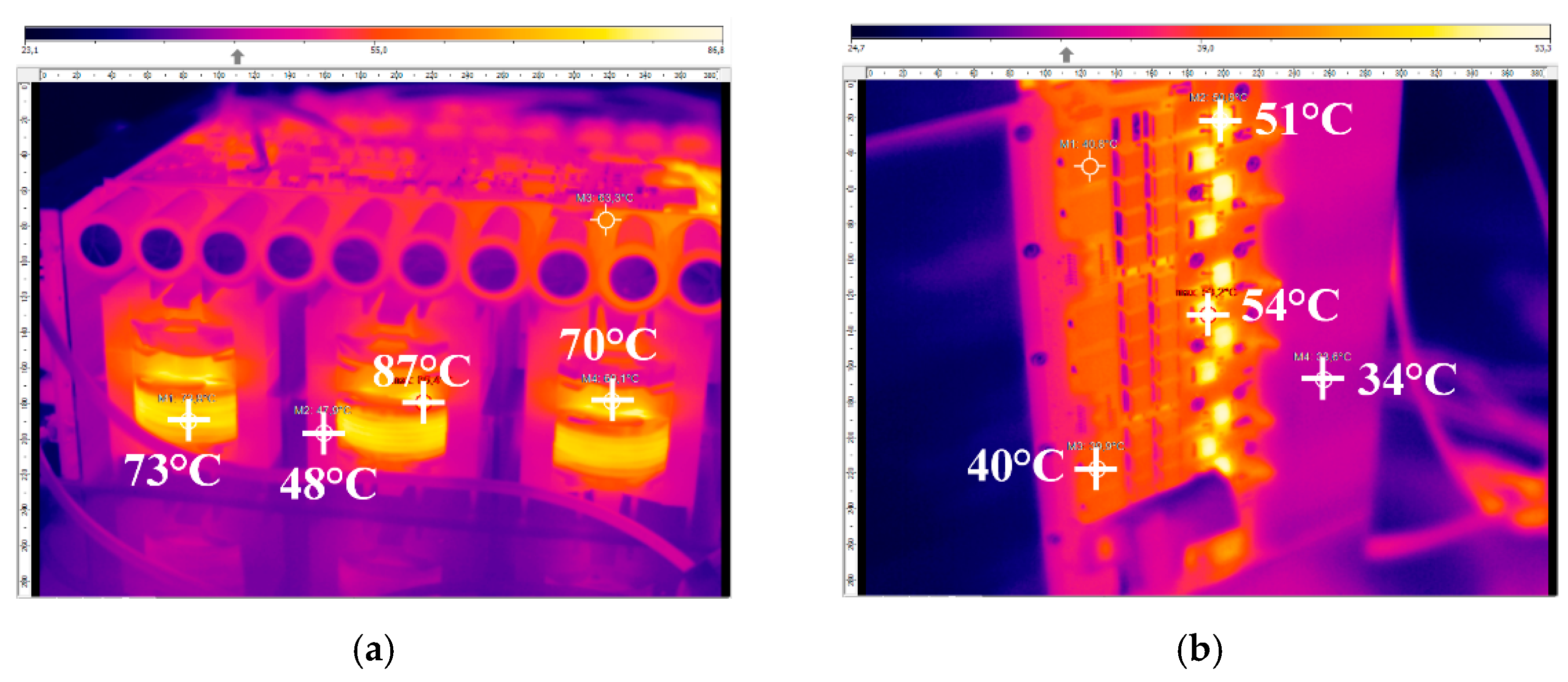
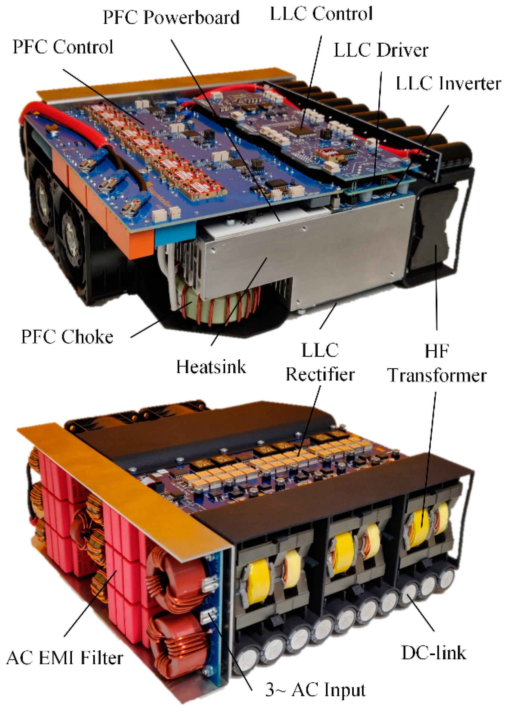
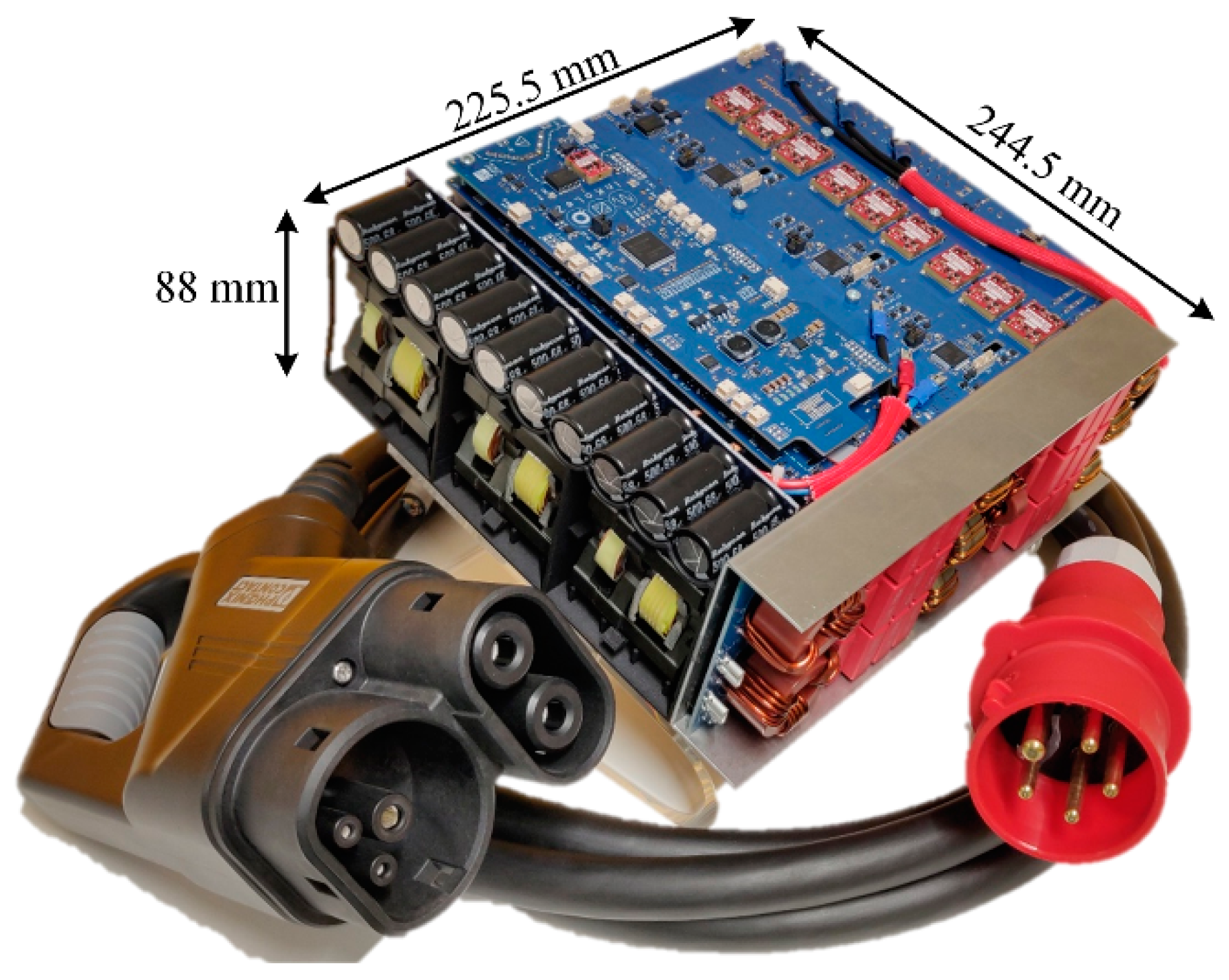
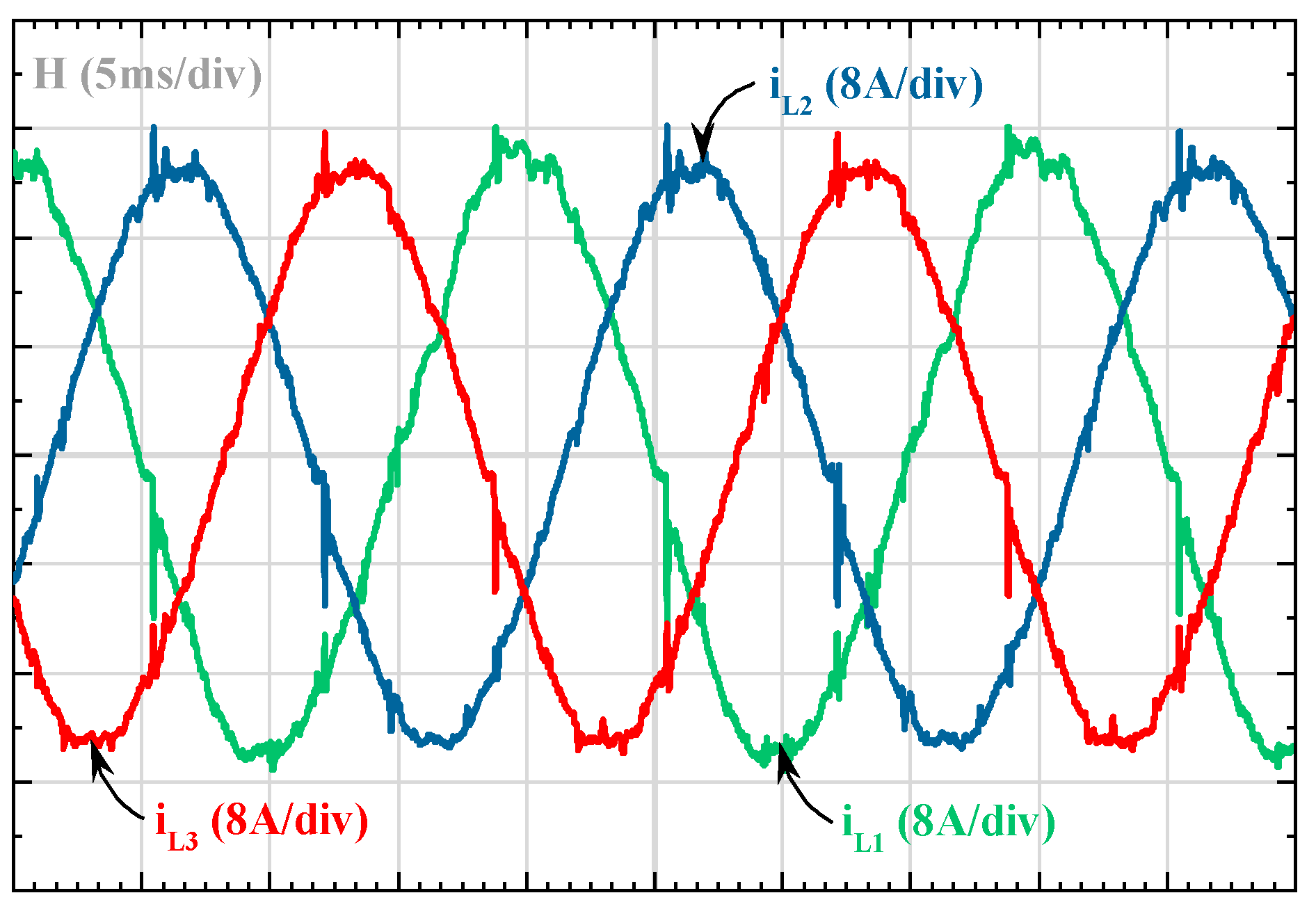
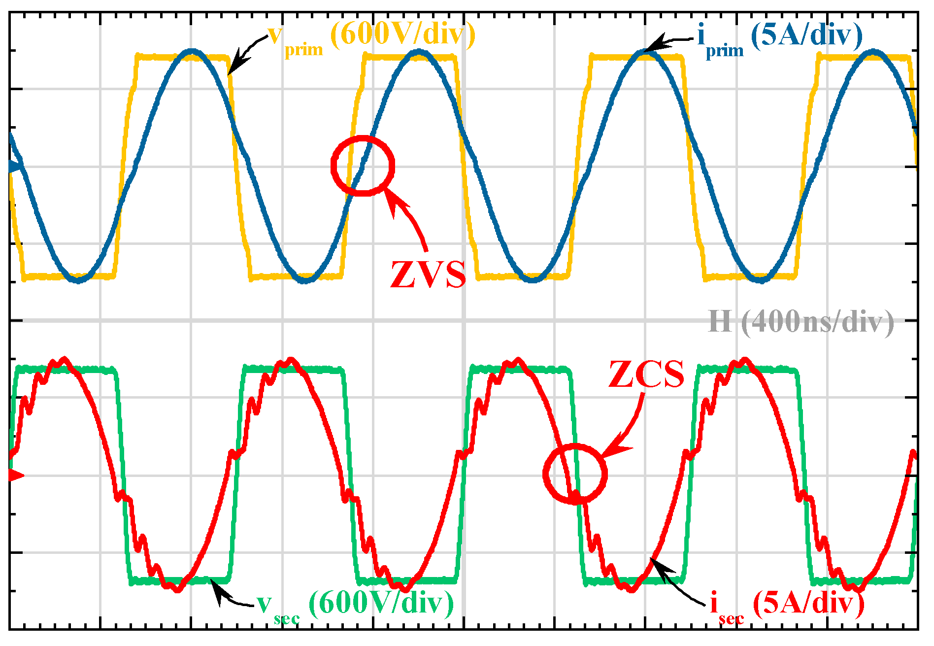
6. Experimental Verification
7. Conclusions
Author Contributions
Funding
Acknowledgments
Conflicts of Interest
References
- Ahmad, A.; Alam, M.S.; Chabaan, R. A Comprehensive Review of Wireless Charging Technologies for Electric Vehicles. IEEE Trans. Transp. Electrif. 2018, 4, 38–63. [Google Scholar] [CrossRef]
- Mahone, A.; Subin, Z.; Orans, R.; Miller, M.; Regan, L.; Calviou, M.; Saenz, M.; Bacalao, N. On the Path to Decarbonization: Electrification and Renewables in California and the Northeast United States. IEEE Power Energy Mag. 2018, 16, 58–68. [Google Scholar] [CrossRef]
- Fulli, G.; Masera, M.; Spisto, A.; Vitiello, S. A Change is Coming: How Regulation and Innovation Are Reshaping the European Union’s Electricity Markets. IEEE Power Energy Mag. 2019, 17, 53–66. [Google Scholar] [CrossRef]
- Khaligh, A.; D’Antonio, M. Global Trends in High-Power On-Board Chargers for Electric Vehicles. IEEE Trans. Veh. Technol. 2019, 68, 3306–3324. [Google Scholar] [CrossRef]
- Li, H.; Zhang, Z.; Wang, S.; Tang, J.; Ren, X.; Chen, Q. A 300-kHz 6.6-kW SiC Bidirectional LLC Onboard Charger. IEEE Trans. Ind. Electron. 2020, 67, 1435–1445. [Google Scholar] [CrossRef]
- Li, B.; Li, Q.; Lee, F.C.; Liu, Z.; Yang, Y. A High-Efficiency High-Density Wide-Bandgap Device-Based Bidirectional On-Board Charger. IEEE J. Emerg. Sel. Top. Power Electron. 2018, 6, 1627–1636. [Google Scholar] [CrossRef]
- Endres, S.; Sessler, C.; Zeltner, S.; Eckardt, B.; Morita, T. 6 kW Bidirectional, Insulated On-board Charger with Normally-Off GaN Gate Injection Transistors. In PCIM Europe 2017; International Exhibition and Conference for Power Electronics, Intelligent Motion, Renewable Energy and Energy Management; VDE: Nuremberg, Germany, 2017; pp. 1–6. [Google Scholar]
- Whitaker, B.; Barkley, A.; Cole, Z.; Passmore, B.; Martin, D.; McNutt, T.R.; Lostetter, A.B.; Lee, J.S.; Shiozaki, K. A High-Density, High-Efficiency, Isolated On-Board Vehicle Battery Charger Utilizing Silicon Carbide Power Devices. IEEE Trans. Power Electron. 2014, 29, 2606–2617. [Google Scholar] [CrossRef]
- Wei, C.; Shao, J.; Agrawal, B.; Zhu, D.; Xie, H. New Surface Mount SiC MOSFETs Enable High Efficiency High Power Density Bi-directional On-Board Charger with Flexible DC-link Voltage. In Proceedings of the 2019 IEEE Applied Power Electronics Conference and Exposition (APEC), Anaheim, CA, USA, 17–21 March 2019; pp. 1904–1909. [Google Scholar]
- Schmenger, J.; Endres, S.; Zeltner, S.; März, M. A 22 kW on-board charger for automotive applications based on a modular design. In Proceedings of the 2014 IEEE Conference on Energy Conversion (CENCON), Johor Bahru, Malaysia, 13–14 October 2014; pp. 1–6. [Google Scholar]
- Gautam, D.S.; Musavi, F.; Edington, M.; Eberle, W.; Dunford, W.G. An Automotive Onboard 3.3-kW Battery Charger for PHEV Application. IEEE Trans. Veh. Technol. 2012, 61, 3466–3474. [Google Scholar] [CrossRef]
- Lu, J.; Liu, G.; Bai, H.; Brown, A.; Johnson, P.M.; McAmmond, M.; Taylor, A.R. Applying Variable-Switching-Frequency Variable-Phase-Shift Control and E-Mode GaN HEMTs to an Indirect Matrix Converter-Based EV Battery Charger. IEEE Trans. Transp. Electrif. 2017, 3, 554–564. [Google Scholar] [CrossRef]
- Tang, Y.; Lu, J.; Wu, B.; Zou, S.; Ding, W.; Khaligh, A. An Integrated Dual-Output Isolated Converter for Plug-in Electric Vehicles. IEEE Trans. Veh. Technol. 2018, 67, 966–976. [Google Scholar] [CrossRef]
- BRUSA Elektronik, AG. NLG667—On Board Fast Charger. Available online: https://www.brusa.biz/produkte/ladetechnik/ladegeraete-750-v/nlg667.html (accessed on 18 March 2020).
- AVID Technology Limited. Onboard Battery Charger: 22kW SAE J1772 On Board Charger Solution for Electric and Hybrid Vehicles, Available with Output Voltage up to 850V. Available online: https://avidtp.com/product/onboard-charger/ (accessed on 29 April 2022).
- FinePower GmbH. Automotive Isolated Onboard Charger for EV/HEV. Available online: https://www.finepower.com/wp-content/uploads/2017/11/Datasheet_Automotive_isolated_onboard-charger_web.pdf (accessed on 29 April 2022).
- Innolectric AG. On-Board Charger: Efficient Power Electronics for AC and DC Charging. On-Board Charger OBC82. Available online: https://innolectric.ag/wp-content/uploads/2020/03/innolectric_On-Board_Charger_E2_2002-1.pdf (accessed on 29 April 2022).
- Stercom GmbH. OnBoard Charger OBC_22kW. Available online: https://stercom.de/en/service/downloads.html (accessed on 24 March 2020).
- Current Ways Inc. CWBC Series 6.6kW Bi-Directional EV On Board Charger. Available online: https://currentways.com/wp-content/uploads/2013/10/CWBC-Series-6.6kW-Bi-directional-OBC-Liquid-Cooled-050918.pdf (accessed on 29 April 2022).
- Current Ways Inc. BC-Series 3kW 112-450 Volt IP67 Rated Air-Cooled EV Battery Charger. Available online: https://currentways.com/wp-content/uploads/2013/10/ds-air-225.pdf (accessed on 29 April 2022).
- Ovar Clean Energy Technology Co., Ltd. EV On-Board Charger: Model CAD332DF-400A 3.3 kW. Available online: https://www.ovartech.com/wp-content/uploads/2017/12/3.3KW-OBC-CAD332DF-400A.pdf (accessed on 29 April 2022).
- Friedli, T.; Hartmann, M.; Kolar, J.W. The Essence of Three-Phase PFC Rectifier Systems—Part II. IEEE Trans. Power Electron. 2014, 29, 543–560. [Google Scholar] [CrossRef]
- Prasad, R.; Namuduri, C.; Kollmeyer, P. Onboard unidirectional automotive G2V battery charger using sine charging and its effect on li-ion batteries. In Proceedings of the 2015 IEEE Energy Conversion Congress and Exposition (ECCE), Montreal, QC, Canada, 20–24 September 2015; pp. 6299–6305. [Google Scholar]
- Jung, C. Power Up with 800-V Systems: The benefits of upgrading voltage power for battery-electric passenger vehicles. IEEE Electrif. Mag. 2017, 5, 53–58. [Google Scholar] [CrossRef]
- Porsche Newsroom. The Charging Process: Quick, Comfortable, Intelligent and Universal. Available online: https://newsroom.porsche.com/en/products/taycan/charging-18558.html (accessed on 28 April 2022).
- Bowermaster, D.; Alexander, M.; Duvall, M. The Need for Charging: Evaluating utility infrastructures for electric vehicles while providing customer support. IEEE Electrif. Mag. 2017, 5, 59–67. [Google Scholar] [CrossRef]
- Liu, Z.; Lee, F.C.; Li, Q.; Yang, Y. Design of GaN-Based MHz Totem-Pole PFC Rectifier. IEEE J. Emerg. Sel. Top. Power Electron. 2016, 4, 799–807. [Google Scholar] [CrossRef]
- Endruschat, A.; Novak, C.; Gerstner, H.; Heckel, T.; Joffe, C.; März, M. A Universal SPICE Field-Effect Transistor Model Applied on SiC and GaN Transistors. IEEE Trans. Power Electron. 2019, 34, 9131–9145. [Google Scholar] [CrossRef]
- Ehrlich, S.; Rossmanith, H.; Sauer, M.; Joffe, C.; März, M. Fast Numerical Power Loss Calculation for High-Frequency Litz Wires. IEEE Trans. Power Electron. 2021, 36, 2018–2032. [Google Scholar] [CrossRef]
- IEC 61851-23:2014; Electric Vehicle Conductive Charging System—Part 23: DC Electric Vehicle Charging Station. IEC: Geneva, Switzerland, 2014.
- IEC 62196-1:2014; Plugs, Socket-Outlets, Vehicle Connectors and Vehicle Inlets—Conductive Charging of Electric Vehicles—Part 1, 2, 3. IEC: Geneva, Switzerland, 2014.
- Phoenix Contact. Charging Technology for Electromobility—Product Overview 2019/2020. Available online: https://www.phoenixcontact.com/assets/2018/interactive_ed/101_142148/epaper/CAT_7_2019_EN_LoRes.pdf (accessed on 28 April 2022).
- Kolar, J.W.; Friedli, T. The Essence of Three-Phase PFC Rectifier Systems—Part I. IEEE Trans. Power Electron. 2013, 28, 176–198. [Google Scholar] [CrossRef]
- Wang, X.; Jiang, C.; Lei, B.; Teng, H.; Bai, H.K.; Kirtley, J.L. Power-Loss Analysis and Efficiency Maximization of a Sili-con-Carbide MOSFET-Based Three-Phase 10-kW Bidirectional EV Charger Using Variable-DC-Bus Control. IEEE J. Emerg. Sel. Top. Power Electron. 2016, 4, 880–892. [Google Scholar] [CrossRef]
- Kolar, J.W.; Zach, F.C. A Novel Three-Phase Three-Switch Three-Level PWM Rectifier. In Proceedings of the 28th Power conversion Conference, Nürnberg, Germany, 28–30 June 1994; pp. 125–138. [Google Scholar]
- Guan, Q.; Li, C.; Zhang, Y.; Wang, S.; Xu, D.D.; Li, W.; Ma, H. An Extremely High Efficient Three-Level Active Neu-tral-Point-Clamped Converter Comprising SiC and Si Hybrid Power Stages. IEEE Trans. Power Electron. 2018, 33, 8341–8352. [Google Scholar] [CrossRef]
- Rodriguez, J.; Lai, J.-S.; Peng, F.Z. Multilevel inverters: A survey of topologies, controls, and applications. IEEE Trans. Ind. Electron. 2002, 49, 724–738. [Google Scholar] [CrossRef] [Green Version]
- Stupar, A.; Friedli, T.; Minibock, J.; Kolar, J.W. Towards a 99% Efficient Three-Phase Buck-Type PFC Rectifier for 400-V DC Distribution Systems. IEEE Trans. Power Electron. 2012, 27, 1732–1744. [Google Scholar] [CrossRef]
- Schrittwieser, L.; Leibl, M.; Haider, M.; Thony, F.; Kolar, J.W.; Soeiro, T.B. 99.3% Efficient Three-Phase Buck-Type All-SiC SWISS Rectifier for DC Distribution Systems. IEEE Trans. Power Electron. 2019, 34, 126–140. [Google Scholar] [CrossRef]
- Heckel, T.; Rettner, C.; März, M. Fundamental efficiency limits in power electronic systems. In Proceedings of the 2015 IEEE International Tele-communications Energy Conference (INTELEC), Osaka, Japan, 18–22 October 2015; pp. 1–6. [Google Scholar]
- Albach, M. Induktivitäten in der Leistungselektronik: Spulen, Trafos und ihre Parasitären Eigenschaften; Springer: Wiesbaden, Germany, 2017; ISBN 978-3-658-15080-8. [Google Scholar]
- IEC 60205:2016; Calculation of the Effective Parameters of Magnetic Piece Parts. IEC: Geneva, Switzerland, 2016.
- Magnetics A Division of Spang & Company. Effects of Temperature on Core Loss of Alloy Powder Cores. Available online: https://www.mag-inc.com/Media/Magnetics/File-Library/Product%20Literature/Powder%20Core%20Literature/Effects-of-Temperature-on-Core-Loss-of-Alloy-Powder-Cores.pdf?ext=.pdf (accessed on 30 May 2022).
- Albach, M.; Durbaum, T.; Brockmeyer, A. Calculating Core Losses in Transformers for Arbitrary Magnetizing Currents a Comparison of Different Approaches. In Proceedings of the PESC Record. 27th Annual IEEE Power Electronics Specialists Conference, Baveno, Italy, 23–27 June 1996; pp. 1463–1468. [Google Scholar]
- Muhlethaler, J.; Biela, J.; Kolar, J.W.; Ecklebe, A. Core Losses Under the DC Bias Condition Based on Steinmetz Parameters. IEEE Trans. Power Electron. 2012, 27, 953–963. [Google Scholar] [CrossRef]
- Albach, M. Two-dimensional calculation of winding losses in transformers. In Proceedings of the 2000 IEEE 31st Annual Power Electronics Spe-cialists Conference. Conference Proceedings (Cat. No.00CH37018), Galway, Ireland, 18–23 June 2000; pp. 1639–1644. [Google Scholar]
- Wang, H.; Dusmez, S.; Khaligh, A. Maximum Efficiency Point Tracking Technique for LLC-Based PEV Chargers Through Variable DC Link Control. IEEE Trans. Ind. Electron. 2014, 61, 6041–6049. [Google Scholar] [CrossRef]
- Deng, J.; Mi, C.C.; Ma, R.; Li, S. Design of LLC Resonant Converters Based on Operation-Mode Analysis for Level Two PHEV Battery Chargers. IEEE/ASME Trans. Mechatron. 2015, 20, 1595–1606. [Google Scholar] [CrossRef]
- Xu, H.; Yin, Z.; Zhao, Y.; Huang, Y. Accurate Design of High-Efficiency LLC Resonant Converter With Wide Output Voltage. IEEE Access 2017, 5, 26653–26665. [Google Scholar] [CrossRef]
- Suryawanshi, H.M.; Talapur, G.G.; Ballal, M.S. Optimized Resonant Converter by Implementing Shunt Branch Element as Magnetizing Inductance of Transformer in Electric Vehicle Chargers. IEEE Trans. Ind. Appl. 2019, 55, 7471–7480. [Google Scholar] [CrossRef]
- He, P.; Mallik, A.; Sankar, A.; Khaligh, A. Design of a 1-MHz High-Efficiency High-Power-Density Bidirectional GaN-Based CLLC Converter for Electric Vehicles. IEEE Trans. Veh. Technol. 2019, 68, 213–223. [Google Scholar] [CrossRef]
- Zhang, Z.; Liu, C.; Wang, M.; Si, Y.; Liu, Y.; Lei, Q. High-Efficiency High-Power-Density CLLC Resonant Converter with Low-Stray-Capacitance and Well-Heat-Dissipated Planar Transformer for EV On-Board Charger. IEEE Trans. Power Electron. 2020, 35, 10831–10851. [Google Scholar] [CrossRef]
- Li, B.; Li, Q.; Lee, F.C. High-Frequency PCB Winding Transformer With Integrated Inductors for a Bi-Directional Resonant Converter. IEEE Trans. Power Electron. 2019, 34, 6123–6135. [Google Scholar] [CrossRef]
- Ren, X.; Xu, Z.; Zhang, Z.; Li, H.; He, M.; Tang, J.; Chen, Q. A 1-kV Input SiC LLC Converter With Split Resonant Tanks and Matrix Transformers. IEEE Trans. Power Electron. 2019, 34, 10446–10457. [Google Scholar] [CrossRef]
- Zou, S.; Lu, J.; Mallik, A.; Khaligh, A. Modeling and Optimization of an Integrated Transformer for Electric Vehicle On-Board Charger Applications. IEEE Trans. Transp. Electrif. 2018, 4, 355–363. [Google Scholar] [CrossRef]
- Zhang, J.; Ouyang, Z.; Duffy, M.C.; Andersen, M.A.E.; Hurley, W.G. Leakage Inductance Calculation for Planar Transformers With a Magnetic Shunt. IEEE Trans. Ind. Appl. 2014, 50, 4107–4112. [Google Scholar] [CrossRef] [Green Version]
- Biela, J.; Kolar, J.W. Electromagnetic integration of high power resonant circuits comprising high leakage inductance transformers. In Proceedings of the 2004 IEEE 35th Annual Power Electronics Specialists Conference, Aachen, Germany, 20–25 June 2004; pp. 4537–4545. [Google Scholar]
- Saket, M.A.; Shafiei, N.; Ordonez, M. LLC Converters With Planar Transformers: Issues and Mitigation. IEEE Trans. Power Electron. 2017, 32, 4524–4542. [Google Scholar] [CrossRef]
- Lazar, J.F.; Martinelli, R. Steady-state analysis of the LLC series resonant converter. In Proceedings of the APEC 2001. Sixteenth Annual IEEE Applied Power Electronics Conference and Exposition (Cat. No.01CH37181), Anaheim, CA, USA, 4–8 March 2001; pp. 728–735. [Google Scholar]
- Ditze, S.; Heckel, T.; März, M. Influence of the junction capacitance of the secondary rectifier diodes on output characteristics in multi-resonant converters. In Proceedings of the 2016 IEEE Applied Power Electronics Conference and Exposition (APEC), Long Beach, CA, USA, 20–24 March 2016; pp. 864–871. [Google Scholar]
- Lu, B.; Liu, W.; Liang, Y.; Lee, F.C.; van Wyk, J.D. Optimal design methodology for LLC resonant converter. In Proceedings of the Twenty-First Annual IEEE Applied Power Electronics Conference and Exposition, 2006. APEC ’06, Dallas, TX, USA, 19–23 March 2006. [Google Scholar] [CrossRef]
- Kundu, U.; Yenduri, K.; Sensarma, P. Accurate ZVS Analysis for Magnetic Design and Efficiency Improvement of Full-Bridge LLC Resonant Converter. IEEE Trans. Power Electron. 2017, 32, 1703–1706. [Google Scholar] [CrossRef]
- Kazimierczuk, M.K.; Czarkowski, D. Resonant Power Converters, 2. Auflage; Wiley-IEEE Press: New York, NY, USA, 2012; ISBN 0470905387. [Google Scholar]
- McLyman, C.W.T. Transformer and Inductor Design Handbook, 3rd ed.; rev. and expanded; Dekker: New York, NY, USA, 2004; ISBN 0824753933. [Google Scholar]
- Li, J.; Abdallah, T.; Sullivan, C.R. Improved calculation of core loss with nonsinusoidal waveforms. In Proceedings of the Conference Record of the 2001 IEEE Industry Applications Conference. 36th IAS Annual Meeting (Cat. No.01CH37248), Chicago, IL, USA, 30 September–4 October 2001; Volume 4, pp. 2203–2210. [Google Scholar] [CrossRef]
- Sullivan, C.R. Optimal choice for number of strands in a litz-wire transformer winding. IEEE Trans. Power Electron. 1999, 14, 283–291. [Google Scholar] [CrossRef] [Green Version]
- Kolar, J.W.; Neumayr, D.; Bortis, D. The Google Little Box Challenge—Ultra-Compact GaN- or SiC-Based Single-Phase DC/AC Power Conversion. In Proceedings of the 19th European Conference on Power Electronics and Applications (EPE’17—ECCE Europe), Warsaw, Poland, 11–14 September 2017. [Google Scholar] [CrossRef]
- Stolzke, T.; Ehrlich, S.; Joffe, C.; März, M. Comprehensive accuracy examination of electrical power loss measurements of inductive components for frequencies up to 1 MHz. J. Magn. Magn. Mater. 2020, 497, 166022. [Google Scholar] [CrossRef]
- Erickson, R.W.; Maksimović, D. Fundamentals of Power Electronics, 2nd ed.; 6 printing; Kluwer Academic Publishers: Norwell, MA, USA, 2004; ISBN 0792372700. [Google Scholar]
- Arshadi, S.A.; Ordonez, M.; Eberle, W.; Saket, M.A.; Craciun, M.; Botting, C. Unbalanced Three-Phase LLC Resonant Converters: Analysis and Trigonometric Current Balancing. IEEE Trans. Power Electron. 2019, 34, 2025–2038. [Google Scholar] [CrossRef]


| Parameter | Value |
|---|---|
| Input voltage Vac | 3~, 400 VAC, 50 Hz |
| Output voltage VBatt | 620–850 VDC |
| Input power Pac | 11 kW |
| Target weight | 5 kg |
| Target volume | 5 L |
| Charging connector | CCS Combo2 |
| Galv. isolation | mandatory |
| Thermal management | forced air-cooling |
| Topology | Voltage Rating (V) | Current Rating (A) | On-State Resistance RDSon (mΩ) |
|---|---|---|---|
| VIENNA | 900 | 11.5 … 35 | 65 … 280 |
| 6S-Boost | 1200 | 30 … 115 | 16 … 75 |
| Parameter | Value |
|---|---|
| Mains voltage Vac | 3~, 400 VAC, 50 Hz |
| DC-link voltage Vlink | 800 VDC |
| Input power Pac | 11 kW |
| Switching frequency fsw,PFC | 50 kHz … 500 kHz |
| PFC inductance LPFC | 10 μH … 300 μH |
| Parameter | Value |
|---|---|
| Core material | High Flux 14 High Flux 26 High Flux 40 High Flux 60 |
| Component volume VTc | 15 cm³ … 75 cm³ |
| Geometry ratio ΘB | 0.1 … 0.9 |
| Geometry ratio ΘC | 0.1 … 1 |
| Switching frequency fsw,PFC | 50 kHz … 200 kHz |
| PFC coil inductance LPFC | 30 μH … 180 μH |
| Parameter | Optimization Result | Prototype |
|---|---|---|
| Core material | High Flux 60 | High Flux 60 |
| ATc | 45.2 mm | 46.7 mm |
| BTc | 24.9 mm | 24.1 mm |
| CTc | 19.2 mm | 18 mm |
| LPFC | 100 μH | 100 μH |
| NPFC | 27 | 27 |
| Winding diameter | 1.6 mm | 1.5 mm |
| Sum core loss | 4.98 W | 4.76 W |
| Sum winding loss | 4.17 W | 4.45 W |
| Total loss PL | 9.15 W | 9.21 W |
| Parameter | Value |
|---|---|
| Input voltage Vdc | 750–900 VDC |
| Output voltage VBatt | 620–850 VDC |
| Number of phases | 3 |
| Nominal output power per phase PLLC,nom | 3.6 kW |
| Switching frequency fsw,LLC | 1 MHz |
| Resonant frequency fsr | 1.02 MHz |
| Primary MOSFET | C3M0065100J |
| Equivalent output capacitance MOSFET Coss | 70 pF |
| Secondary diode | IDM10G120G5 |
| Equivalent output capacitance diode Cj | 60 pF |
| Dead time tdead | 100 ns |
| Transformer turns ratio n | 1.06:1 |
| Resonant capacitance Cres | 1.62 nF |
| Resonant inductance Lres | 15 μH |
| Magnetizing inductance Lm | 39 μH |
| Target volume of transformer and inductance | 0.1 L |
| Parameter | Range |
|---|---|
| Transformer: number of turns (primary) Np | 5, 10, 16, 20 |
| Transformer: number of turns (secondary) Ns | 5, 10, 16, 20 |
| Resonance inductor: number of turns Nres | 1 … 10 |
| Core geometry ratio χBA | 0.2 … 2 |
| Core geometry ratio χCA | 0.2 … 2 |
| Winding window ratio χw | 0.1 … 0.9 |
| Filling factor of Litz wire in the winding window ρw | 0.05 … 0.7 |
| Volumes VEc,tr, VEc,res | 0.01 L … 1 L |
| Loss (W) | 3D Simulation | Measurement |
|---|---|---|
| Transformer winding loss | 9.3 | - |
| Inductor winding loss | 2.4 | - |
| Sum winding loss | 11.7 | 10.5 |
| Transformer core loss | 6.4 | - |
| Inductance core loss | 4.5 | - |
| Sum core loss | 10.9 | - |
| Total loss | 22.6 | 23.8 |
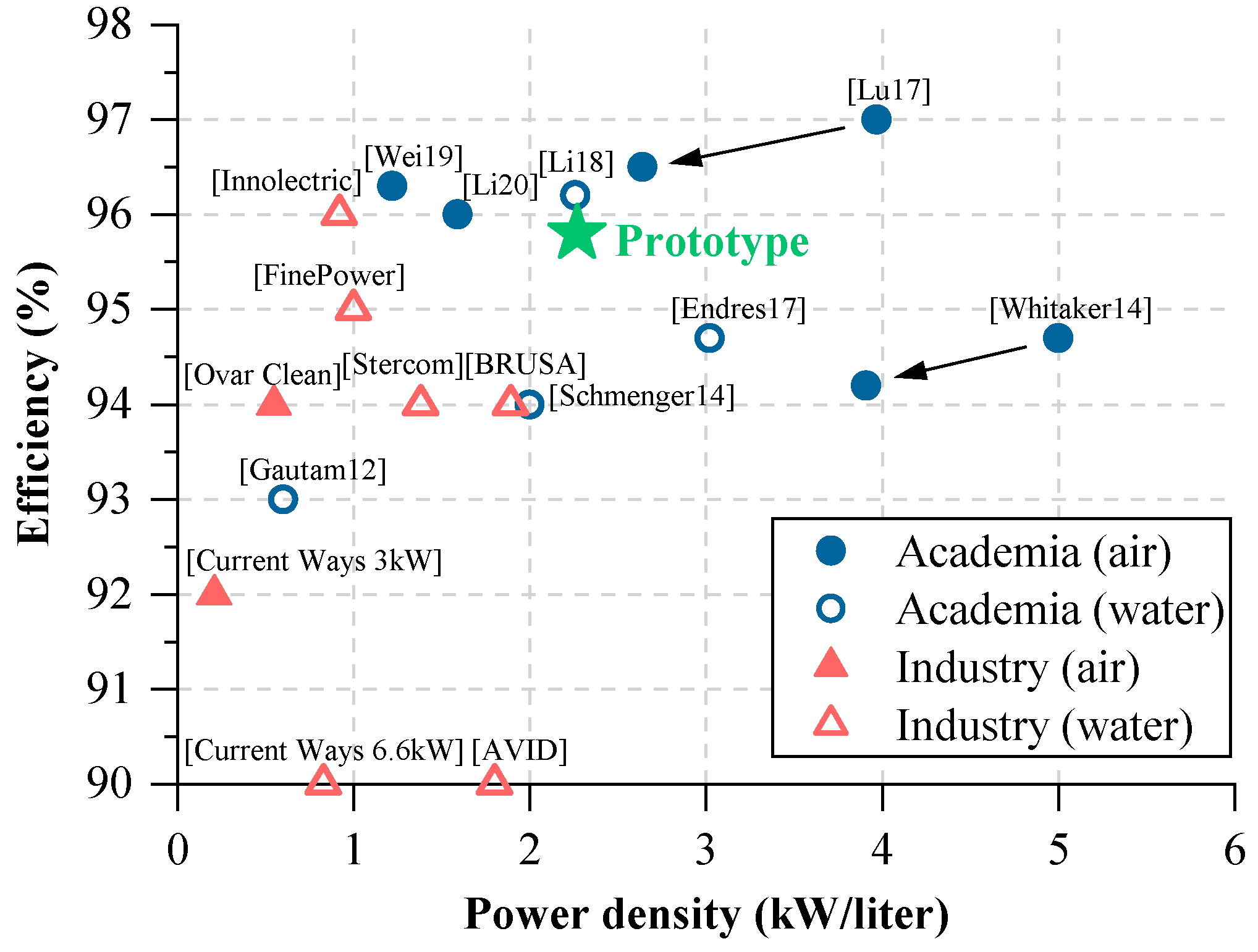
| References | Efficiency (%) | Cooling | Characteristics |
|---|---|---|---|
| [5] | 96 | air-cooled |
|
| [6] | 96.2 | water-cooled |
|
| [7] | 94.7 | water-cooled |
|
| [8] | 94.7 | air-cooled |
|
| [9] | 96 | air-cooled |
|
| [10] | 94 | water-cooled |
|
| [12] | 97 | air-cooled |
|
| Our proposal | 95.8 | air-cooled |
|
Publisher’s Note: MDPI stays neutral with regard to jurisdictional claims in published maps and institutional affiliations. |
© 2022 by the authors. Licensee MDPI, Basel, Switzerland. This article is an open access article distributed under the terms and conditions of the Creative Commons Attribution (CC BY) license (https://creativecommons.org/licenses/by/4.0/).
Share and Cite
Ditze, S.; Ehrlich, S.; Weitz, N.; Sauer, M.; Aßmus, F.; Sacher, A.; Joffe, C.; Seßler, C.; Meißner, P. A High-Efficiency High-Power-Density SiC-Based Portable Charger for Electric Vehicles. Electronics 2022, 11, 1818. https://doi.org/10.3390/electronics11121818
Ditze S, Ehrlich S, Weitz N, Sauer M, Aßmus F, Sacher A, Joffe C, Seßler C, Meißner P. A High-Efficiency High-Power-Density SiC-Based Portable Charger for Electric Vehicles. Electronics. 2022; 11(12):1818. https://doi.org/10.3390/electronics11121818
Chicago/Turabian StyleDitze, Stefan, Stefan Ehrlich, Nikolai Weitz, Marco Sauer, Frank Aßmus, Anne Sacher, Christopher Joffe, Christoph Seßler, and Patrick Meißner. 2022. "A High-Efficiency High-Power-Density SiC-Based Portable Charger for Electric Vehicles" Electronics 11, no. 12: 1818. https://doi.org/10.3390/electronics11121818
APA StyleDitze, S., Ehrlich, S., Weitz, N., Sauer, M., Aßmus, F., Sacher, A., Joffe, C., Seßler, C., & Meißner, P. (2022). A High-Efficiency High-Power-Density SiC-Based Portable Charger for Electric Vehicles. Electronics, 11(12), 1818. https://doi.org/10.3390/electronics11121818