Article

Design and Verification of a Charge Pump in Local Oscillator for 5G Applications

1
State Key Laboratory of Electronic Thin Films and Integrated Devices, University of Electronic Science and Technology of China, Chengdu 610054, China
2
School of Electronic Engineering, Soochow University, Suzhou 215000, China
*
Author to whom correspondence should be addressed.
Electronics 2021, 10(9), 1009; https://doi.org/10.3390/electronics10091009
Submission received: 28 March 2021 / Revised: 19 April 2021 / Accepted: 22 April 2021 / Published: 23 April 2021
(This article belongs to the Special Issue Millimeter-Wave Integrated Circuits and Systems for 5G Applications)

Abstract

:
A charge pump (CP) that has low current mismatch to reduce the locking time of the Phase-Locked Loop (PLL) is proposed. The design is promising in 5G applications with the capabilities of fast settling and low power consumption. In this design, a charge pump architecture consists of an operational power amplifier (OPA), switches, three D flip-flops (DFFs) and passive devices. A phase error compensation technique is introduced in the charge pump to reduce the locking time. The current mismatch, which is mainly due to the leakage current, is below 1% for a large output voltage headroom of 84% of the supply voltage. An 18.4% reduction in the settling time is realized by the proposed design.

1. Introduction

A phase-locked loop (PLL)-based frequency synthesizer is a vital component in communication systems [1,2]. To support the high data-rate transmission in 5G systems, the stringent requirements of being both fast settling with low power consumption must be satisfied. Owing to its wide locking range and low phase offset, the charge pump (CP) PLL is widely used in practice [3,4,5]. However, the current mismatch in charge pump eventually leads to static phase offsets and reference spurs, which is a main issue in PLL design. Many approaches have been proposed to reduce the mismatch between the injected current and removed current. The work reported in [6] used the active feedback circuit based operational power amplifier (OPA) to increase output resistance and reduce current mismatch. However, with an extra OPA circuit, the power consumption would be increased. Report [7] proposed a method in which the control words are used to calibrate the current mismatch. The complexity of the whole CP was increased vastly. These methods greatly increase the complexity of charge pumping. A self-tracking CP was proposed in [8], but the technique was limited by PVT (Process Voltage Temperature). To achieve the possible largest frequency range, ideally, the CP output voltage should be in the range of 0 to the supply voltage to maximize the use of the oscillator tuning range. Being fast settling with no data loss during frequency locking is required for the high data-rate transmission in 5G applications. The fast-locking capability is particularly critical for systems requiring a frequency-hopping operation. The main idea of reducing the settling time is to widen (narrow) the loop bandwidth in locking (locked state). Several strategies are employed to adjust bandwidth-dependent parameters/components, such as the CP current/low pass filter (LPF). Reference [9] straightly used two sets of CP and switches to adjust the current and resistance values of LPF. Reference [10] combined the programmable divider with sets of CP to compensate for phase error. Though the above methods could improve the locking speed, more transistors are needed, and the design complexity is increased.
In this work, a phase-locked loop charge pump, which has low current mismatch and reduced locking time, is proposed. The current mismatch is reduced to less than 1% for a voltage headroom from 0.4 V to 4.6 V. A phase error compensation module is also employed in the design. The locking time is reduced by 18.4% with low complexity and circuit cost.

2. Design of Low Current Mismatch Charge Pump with Broad Voltage Headroom

To support high data-rate 5G application, the settling time is always expected to be reduced as much as possible. Modulating the bandwidth to accelerate the locking process is the main strategy. As shown in Figure 1a, the bandwidth is hard to be controlled when the parameters and structures of CP, voltage-controlled oscillator (VCO), LPF and divider are fixed. As the CP current is positively related to the bandwidth, an adjustable charge pump is proposed to reduce the settling time as shown in Figure 1b. The proposed CP should be able to maintain a low current mismatch while having a broad voltage headroom. It could also be modulated by the phase error compensation module to reduce the settling time.
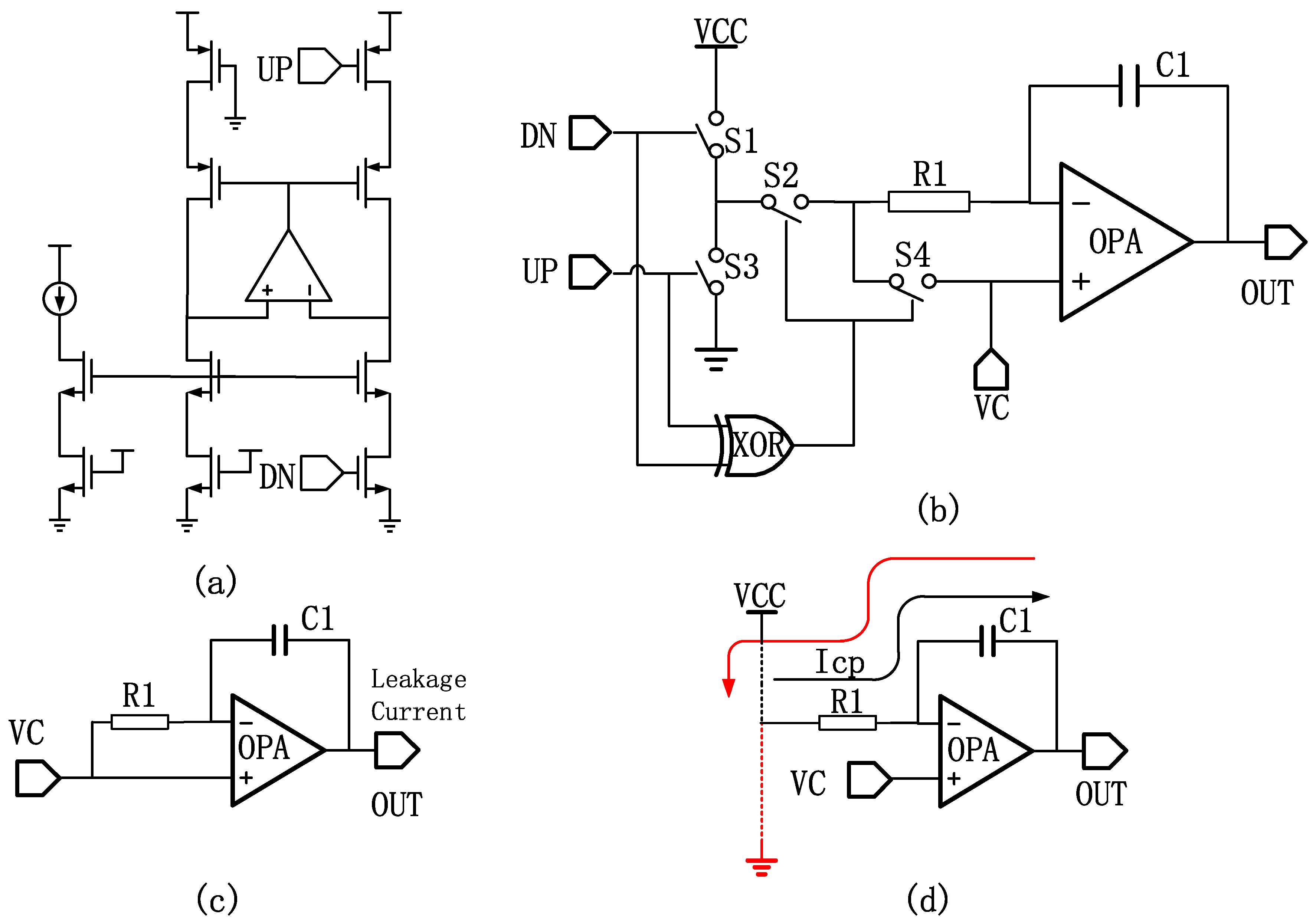
Compared with the traditional OPA-based CP in Figure 2a, the current sink and current source have been eliminated in the proposed design Figure 2b. In the locking mode, static power consumption is saved. Moreover, in the proposed design, with the help of OPA, charge sharing issues are no longer significant. The charging signal “UP” and discharging signal “DN”, which are the output signals of the phase frequency detector, are at high and low voltage levels, respectively. When the loop is locked, Switches S1, S2 and S3 are switched off while S4 is switched on. For the virtual-short and virtual-off features, there are no current flows through R1. Therefore, the output voltage (VOUT) of CP can be expressed as the following:
V O U T = V C + Q O U T / C C 1
The output voltage of CP is maintained and influenced only by the leakage current as shown in Figure 2c. When the phase and frequency of signal “Fdiv” are faster and higher than that of signal “Fref”, respectively, both signals UP and DN are set to the low level. Then, S3 and S4 are switched off; S1 and S2 are switched on as shown in Figure 2d with a black line. The discharging current and time-dependent output voltage can be obtained as the following:
I D N = ( V C C V C ) / R
V O U T ( t ) = V O U T ( I D N · t ) / C C 1
On the other hand, as shown in Figure 2d with a red line, the charging current and time-dependent output voltage can be obtained as follows:
I U P = V C / R
V O U T ( t ) = V O U T + ( I U P · t ) / C C 1
When the voltage of VC is set to half of VCC, the charging and discharging currents have the same magnitude.
Compared with the traditional OPA-based CP shown in Figure 2a, the primary power consumption is reduced and dependent on the OPA in the locking mode. The control voltage range is extended without considering the current mismatch caused by the PMOS and NMOS.

3. Design of Simplified Charge Pump for Fast Locking PLL

As discussed above, the primary approach for reducing the locking time relies on adjusting the bandwidth during the locking process and at the locked state. However, as shown in Figure 1a, when the structures of LPF, VCO gain and CP current are fixed, it is hard to modulate the bandwidth. The LPF has passive devices which are hard to switch and that occupy more area. The VCO design is independent of the bandwidth. A current control module is needed for the design as shown in Figure 1. When the structure and parameters of the LPF are fixed, the bandwidth of the PLL mainly depends on the current of CP. According to Equations (2) and (4), the bandwidth can be varied with the DC voltage, VC. Then, TDC and common-mode voltage selection modules are added to reduce the settling time.
TDC (Time to Digital Converter) is used to capture the phase information in practical design [10,11,12,13]. As shown in Figure 3, DFF (D flip-flop) is used as the delay cell, which has delayed time T to quantize the phase error.
The positions of the rising edge and falling edge indicate the size of the phase error and polarity, as shown in Figure 4. The binary string ‘001’ or ‘011’ indicates that signal “Fdiv” is faster than signal “Fref”. On the other hand, the binary string ‘100’ or ‘110’ indicates that signal “Fref” is faster than signal “Fdiv”. The rest of the binary strings are not assigned to contribute to the whole loop. The binary strings are decoded as different DC voltages, which are assigned to common-mode voltage VC as shown in Figure 4.
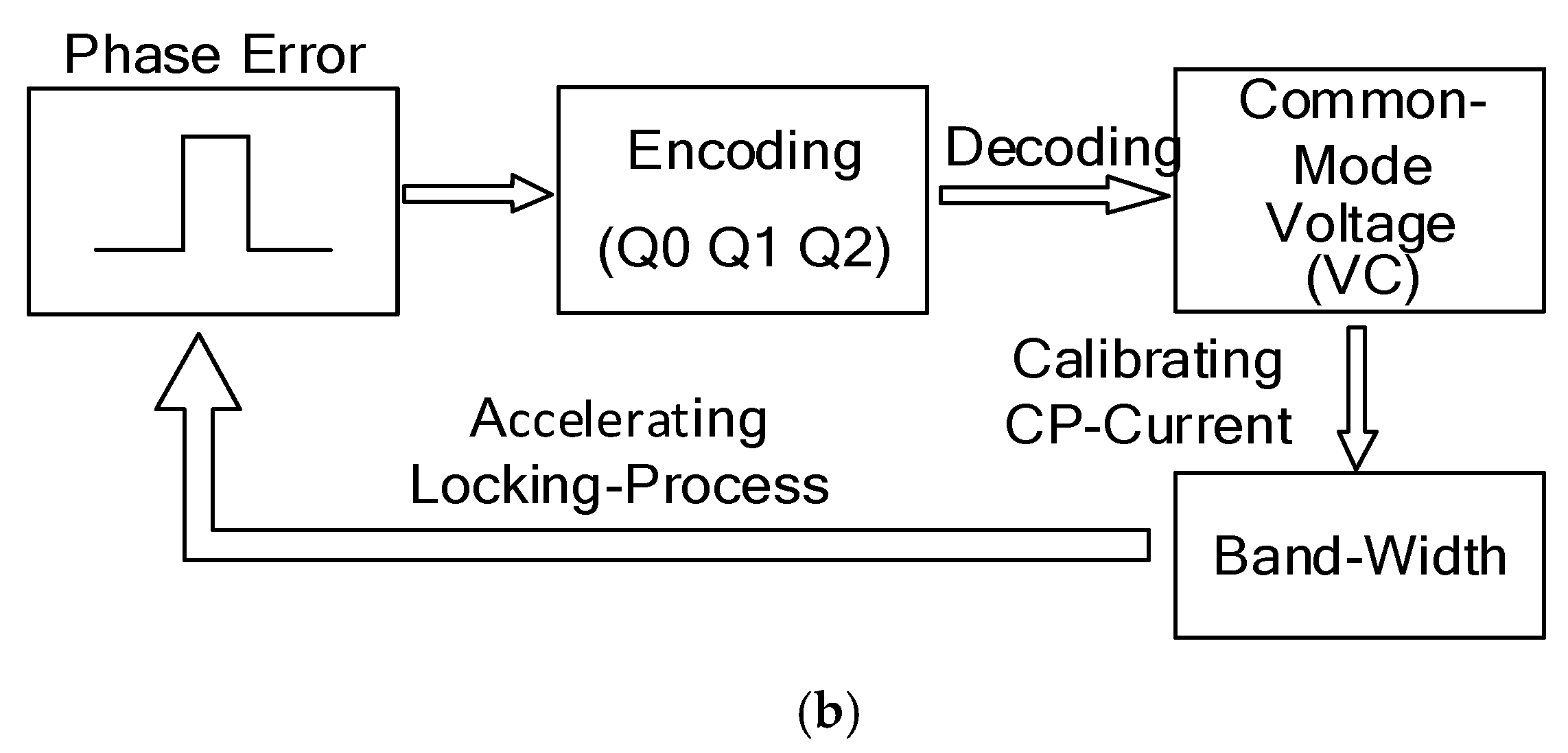
The decoded common-mode voltages are used to adjust the bandwidth of the loop by changing the current of the CP as shown in Figure 3. When the phase error between “Fref” and “Fdiv” is less than 2T, the loop enters the fast-locking process. When “Fdiv” is faster than “Fref” and the phase error falls in the range of (T, 2T), the common-mode voltage VC is assigned with 0.3 VDD. The discharging current can be obtained as follows:
I D N = ( V C C 0.3 V C C ) / R
The bandwidth is widened by the enlarged discharging current IDN and the settling time can be reduced. By varying the voltage of VC, the current of CP is increased or decreased to accelerate the locking process.
When the number of delay cells in TDC increases, the resolution of TDC can be improved, but a larger power consumption and chip area are required. In the present design, only three delay cells are utilized to demonstrate the theory of reducing locking time. If the delay time is set to small, TDC works only at the part of the near-locking process. If the delay time is set to a large value, the TDC works only at the beginning of the near-locking process. Then, there is a trade-off between the power consumption, the unit delay time of TDC, and the number of delay cells. All of these parameters can be adjusted according to the applications. The delay time is set to 7 ns in the present design when the period time is 100 ns.

4. Simulation and Experimental Results

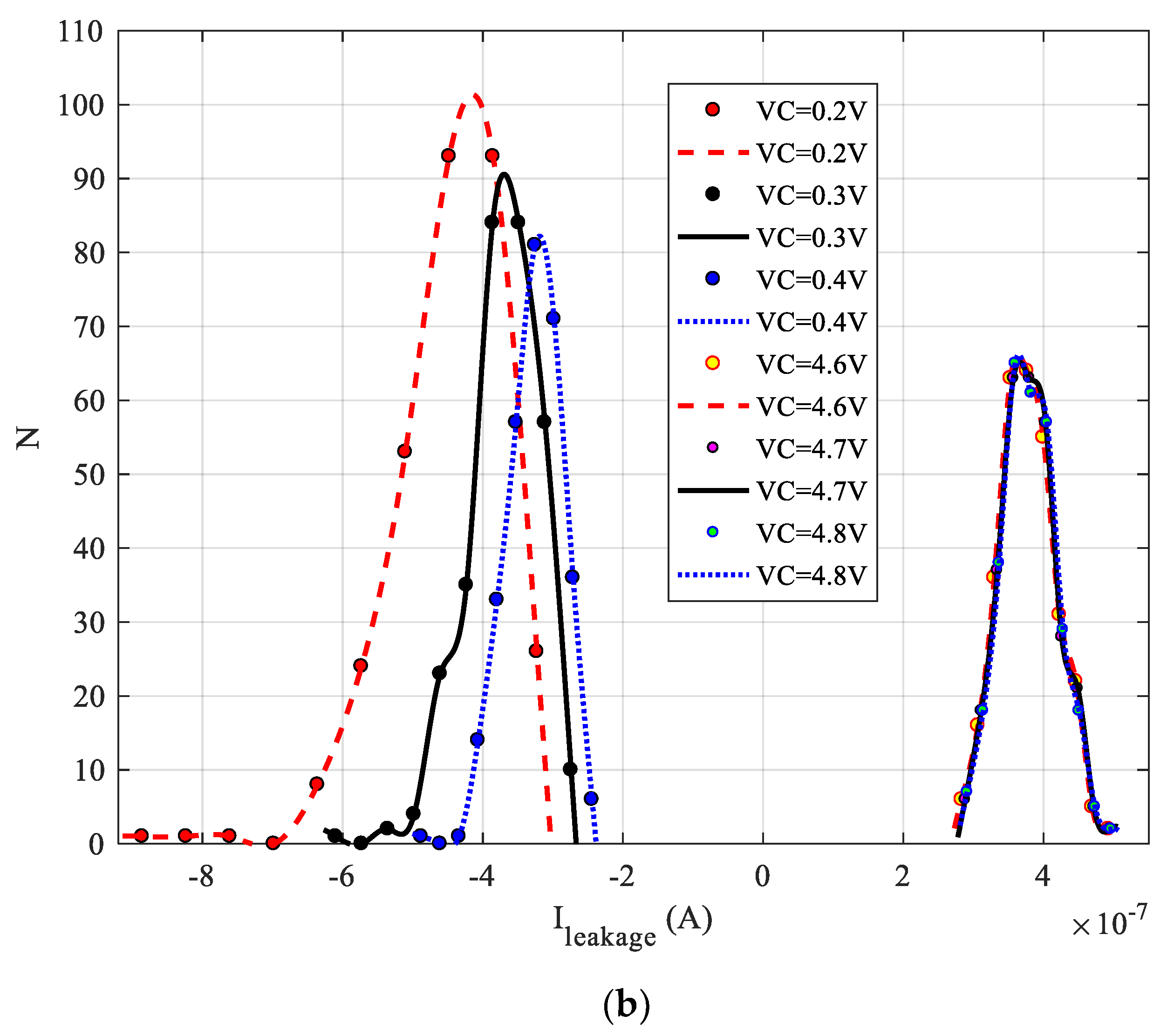
Compared with the traditional CP structure, there is no current mismatch between the injected current and removed current in the locked phase in the proposed design. Only the leakage current affects the stability of the control voltage of the VCO. When the common voltage of OPA is varied with the phase error, the variation of the leakage current is as shown in Figure 5a. Though the signal VC is set to the range of (1.5 V, 3.5 V) in this design, the leakage current is acceptable in a broad output voltage headroom of (0.4 V, 4.6 V). The leakage current is reduced to less than 400 nA in range, but rises dramatically when VC is out of range.
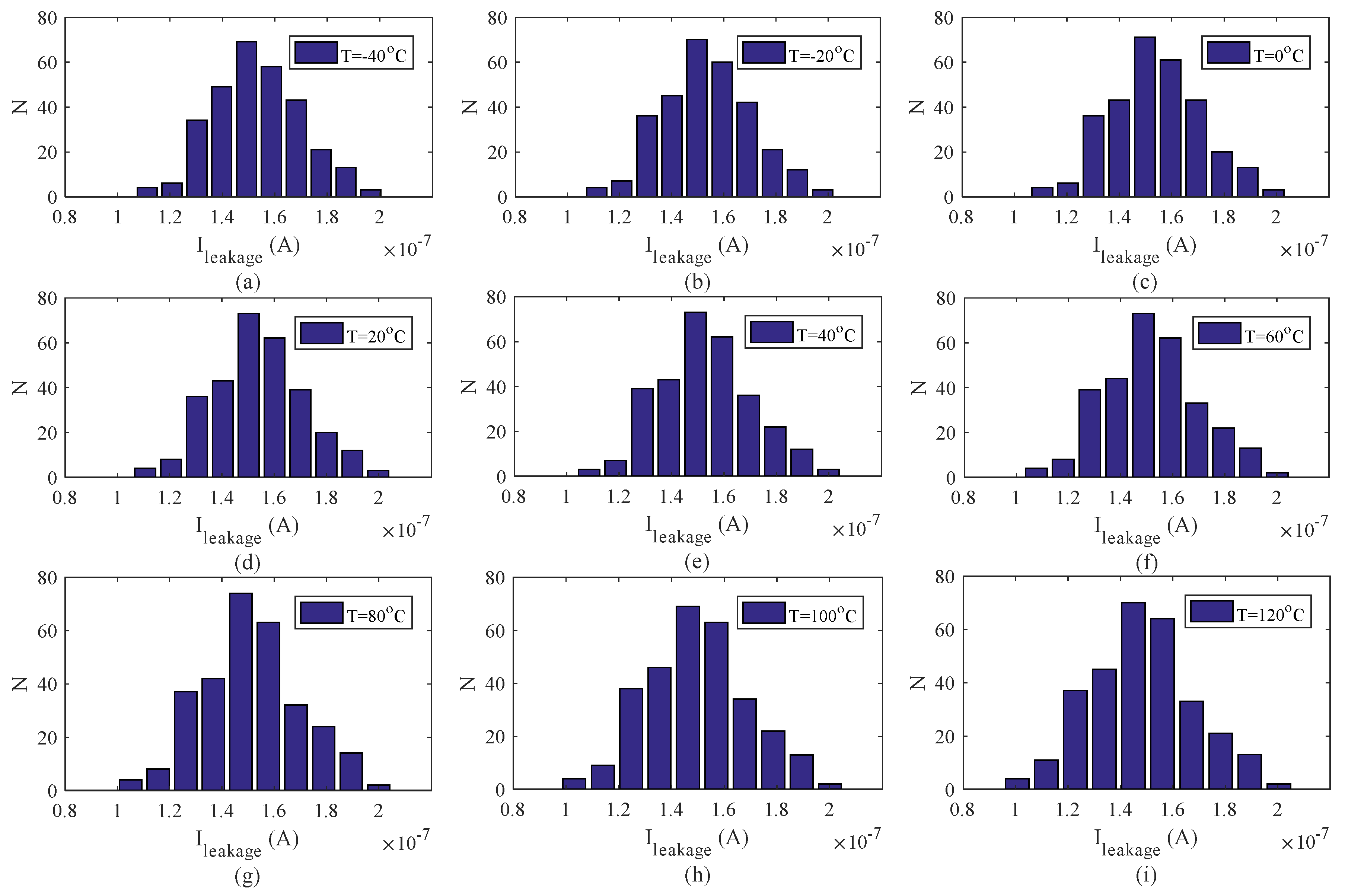
As shown in Figure 6, the current mismatch is below 1% (500 nA) for a broad output voltage headroom of 84% of the supply voltage. As shown in Figure 7, the distribution of the leakage current is little affected by temperature.
The leakage current and output voltage range are the major factors in the CP design. The output voltage range always varies from 66.6% to 83.3% (Table 1). An 84% output voltage range was achieved in this design. When the source and sink currents are eliminated, the output voltage range is enlarged. Then, the leakage current in the source and sink currents are also eliminated. Compared with other works, the leakage current in this work is below 1%, which is quite acceptable. The whole area of the PLL core is 0.55 mm × 0.6 mm, as shown in Figure 8.
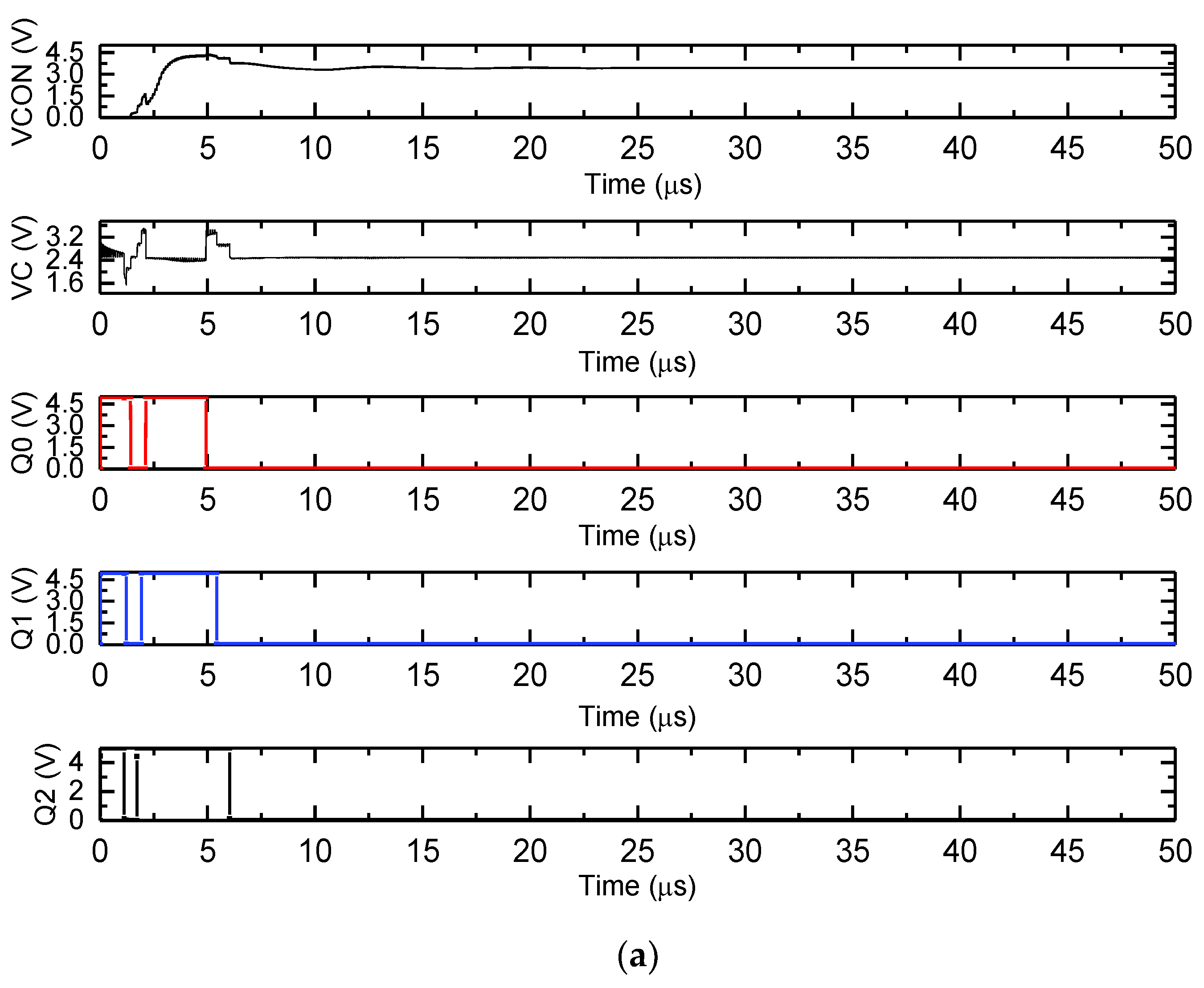
Inspired by the phase error compensation technique, a 3-bit TDC is constructed. It switches the common voltage VC to accelerate the locking process, as shown in Figure 9a. According to Figure 9b, the magnitude of VC is assigned by the decoded binary string ‘Q0Q1Q2′. The control voltage of the VCO is calibrated by the common mode voltage VC to limit the phase error of the PFD to less than T. During the fast-locking mode, the phase error is monitored and reduced through compensation.
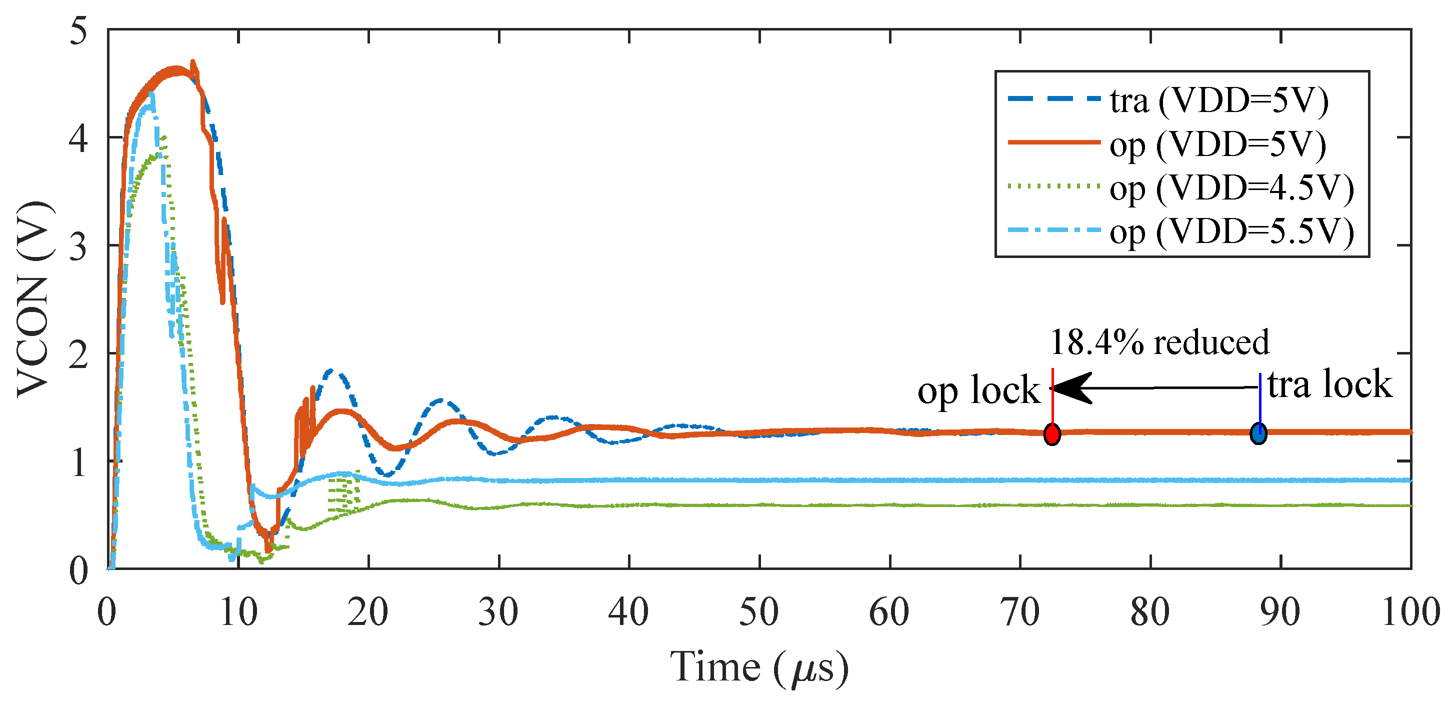
Figure 10 shows the comparison of the simulated settling time between the optimized CP in the present design and the traditional CP without phase error compensation under different supply voltages. The results presented in Figure 10 were obtained from the schematic simulations. Compared with the traditional CP without phase error compensation, the optimized CP of the present design reduces the phase error of the PFD, leading to a decrease in the settling time from 89.6 μs to 73.1 μs. In the present design, only a 3-bit TDC was used to quantize and encode the phase error. With an increase in the bit number of the TDC, the delay time T decreases, and the locking capability can be further improved.

5. Conclusions

In this work, a PLL charge pump with a low current mismatch for reducing locking time is proposed. The current mismatch caused by leakage current is below 1% for a broad output voltage headroom of 84% of the supply voltage. Based on an OPA, with the technique of phase error compensation, reduction of the settling time by 18.4% is achieved.

Author Contributions

Conceptualization, R.G.; methodology, R.G.; software, R.G.; validation, R.G.; formal analysis, Z.L. and S.H.; investigation, R.G.; resources, Q.Y.; data curation, R.G.; writing—original draft preparation, R.G.; writing—review and editing, R.G., Y.L. and L.R.; supervision, Y.L. and L.R.; project administration, Y.L. and L.R.; funding acquisition, Y.L. and L.R. All authors have read and agreed to the published version of the manuscript.

Funding

This work was supported by NSFC under project No. 61774028, 92064004 and 61771097.

Conflicts of Interest

The authors declare no conflict of interest.

References

  1. Han, F.; Gao, J.; Li, X.; Chen, Z. A Four-Channel CMOS Front-End for Interference-Robust GNSS Receiver. Electronics 2020, 9, 291. [Google Scholar] [CrossRef] [Green Version]
  2. Sánchez-Azqueta, C.; Guerrero, E.; Gimeno, C.; Celma, S. A Reconfigurable Radio-Frequency Converter IC in 0.18 µm CMOS. Electronics 2019, 8, 1146. [Google Scholar] [CrossRef] [Green Version]
  3. Ali, E.; Hangmann, C.; Hedayat, C.; Haddad, F.; Rahajandraibe, W.; Hilleringmann, U. Event driven modeling and characterization of the second order voltage switched charge pump pll. IEEE Trans. Circuits Syst. I: Regul. Pap. 2016, 63, 347–358. [Google Scholar] [CrossRef]
  4. Kim, K.; Yoo, C. A fREF/5 bandwidth type-ii chargepump phase-locked loop with dual-edge phase comparison and sampling loop filter. IEEE Microw. Wirel. Compon. Lett. 2018, 28, 825–827. [Google Scholar] [CrossRef]
  5. Homayoun, A.; Razavi, B. On the stability of chargepump phase-locked loops. IEEE Trans. Circuits Syst. I: Regul. Pap. 2016, 63, 741–750. [Google Scholar] [CrossRef]
  6. Choi, Y.S.; Han, D.H. Gain-boosting charge pump for current matching in phase-locked loop. IEEE Trans. Circuits Syst. II: Express Briefs 2006, 53, 1022–1025. [Google Scholar] [CrossRef]
  7. Lin, W.M.; Liu, S.I.; Kuo, C.H.; Li, C.H.; Hsieh, Y.J.; Liu, C.T. Aphase-locked loop with self-calibrated charge pumps in 3-m ltps-tft technology. IEEE Trans. Circuits Syst. II: Express Briefs 2009, 56, 142–146. [Google Scholar]
  8. Chen, Y.; Mak, P.I.; Zhou, Y. Self-tracking charge pump for fast-locking pll. Electron. Lett. 2010, 46, 755–757. [Google Scholar] [CrossRef]
  9. Yang, C.Y.; Liu, S.I. Fast-switching frequency synthesizer with a discriminator-aided phase detector. IEEE J. Solid-State Circuits 2000, 35, 1445–1452. [Google Scholar] [CrossRef]
  10. Chiu, W.H.; Huang, Y.H.; Lin, T.H. A dynamic phase error compensation technique for fast-locking phase-locked loops. IEEE J. Solid-State Circuits 2010, 45, 1137–1149. [Google Scholar] [CrossRef]
  11. Yao, C.W.; Ni, R.; Lau, C.; Wu, W.; Godbole, K.; Zuo, Y.; Ko, S.; Kim, N.-S.; Han, S.; Jo, I.; et al. A 14-nm 0.14-ps rms fractional-n digital pll with a 0.2-ps resolution adcassisted coarse/fine-conversion chopping tdc and tdc nonlinearity calibration. IEEE J. Solid-State Circuits 2017, 52, 3446–3457. [Google Scholar] [CrossRef]
  12. Wu, Y.; Shahmohammadi, M.; Chen, Y.; Lu, P.; Staszewski, R.B. A 3.5–6.8-ghz wide-bandwidth dtc-assisted fractional-n all-digital pll with a mash -tdc for low inband phase noise. IEEE J. Solid-State Circuits 2017, 52, 1885–1903. [Google Scholar] [CrossRef]
  13. Lee, M.; Kim, S.; Park, H.J.; Sim, J.Y. A 0.0043-mm 2 0.3–1.2-v frequency-scalable synthesized fractional-n digital pll with a speculative dual-referenced interpolating tdc. IEEE J. Solid-State Circuits 2018, 54, 99–108. [Google Scholar] [CrossRef]
  14. Liu, P.; Sun, P.; Jung, J.; Heo, D. Pll charge pump with adaptive body-bias compensation for minimum current variation. Electron. Lett. 2012, 48, 16–18. [Google Scholar] [CrossRef]
  15. Hwang, M.S.; Kim, J.; Jeong, D.K. Reduction of pump current mismatch in charge-pump pll. Electron. Lett. 2009, 45, 135–136. [Google Scholar] [CrossRef]
  16. Jalalifar, M.; Byun, G.S. Near-threshold charge pump circuit using dual feedback loop. Electron. Lett. 2013, 49, 1436–1438. [Google Scholar] [CrossRef]
  17. Joram, N.; Wolf, R.; Ellinger, F. High swing pll charge pump with current mismatch reduction. Electron. Lett. 2014, 50, 661–663. [Google Scholar] [CrossRef]
Figure 1. The main structure of (a) a traditional PLL design, and (b) the proposed CP in PLL.
Electronics 10 01009 g001
Figure 2. (a) Structure of a traditional OPA-based CP; (b) circuit schematic of the optimized CP; (c) the optimized CP in locking mode; and (d) the optimized CP in discharging/charging mode.
Electronics 10 01009 g002
Figure 3. The transformation between phase error and common-mode voltage.
Electronics 10 01009 g003
Figure 4. The timing diagram of the sampling circuit.
Electronics 10 01009 g004
Figure 5. (a) Variation of the leakage current with the common mode voltage, and (b) leakage current corresponding to extended VC.
Electronics 10 01009 g005aElectronics 10 01009 g005b
Figure 6. Distribution of leakage current for various common mode voltages. The result is obtained from Monte Carlo simulation with 300 points.
Electronics 10 01009 g006
Figure 7. Distribution of leakage current Ileakage for VC = 2.5 V at various temperatures: (a) −40 °C, (b) −20 °C, (c) 0 °C, (d) 20 °C, (e) 40 °C, (f) 60 °C, (g) 80 °C, (h) 100 °C and (i) 120 °C.
Electronics 10 01009 g007
Figure 8. Layout of the proposed PLL.
Electronics 10 01009 g008
Figure 9. (a) Simulated PLL lock process optimized by the proposed CP; and (b) the workflow of the PLL locking process.
Electronics 10 01009 g009aElectronics 10 01009 g009b
Figure 10. The simulated settling time of the optimized CP and traditional CP without phase error compensation under different supply voltages.
Electronics 10 01009 g010
Table 1. State-of-the-art compensated PLL charge pumps.
Items[14][15][16][17]This Work
Technology node (nm)180130130180250
Current mismatch (%)≤0.9≤1.7≤1≤2.1≤1
Output voltage range (V, %)0.2–1, 66.60.2–1, 66.60.1–0.48, 760.2–2.7, 83.30.4–4.6, 84
Supply voltage (V)1.21.20.535
compensation methodBody-bias compensationDual compensation circuitsDual feedback loop3 Rail-to-rail OPsElimination of source and sink currents
Publisher’s Note: MDPI stays neutral with regard to jurisdictional claims in published maps and institutional affiliations.