Article

Wideband Reconfigurable Integrated Low-Pass Filter for 5G Compatible Software Defined Radio Solutions

Micro and Nanoelectronics Systems Design and Research Laboratory, Vilnius Gediminas Technical University, 10257 Vilnius, Lithuania
*
Author to whom correspondence should be addressed.
Electronics 2021, 10(6), 734; https://doi.org/10.3390/electronics10060734
Submission received: 8 February 2021 / Revised: 12 March 2021 / Accepted: 16 March 2021 / Published: 19 March 2021
(This article belongs to the Special Issue Analog Microelectronic Circuit Design and Applications)

Abstract

:
This article presents a wideband reconfigurable integrated low-pass filter (LPF) for 5G NR compatible software-defined radio (SDR) solutions. The filter uses Active-RC topology to achieve high linearity performance. Its bandwidth can be tuned from 2.5 MHz to 200 MHz, which corresponds to a tuning ratio of 92.8. The order of the filter can be changed between the 2nd, 4th, or 6th order; it has built-in process, voltage, and temperature (PVT) compensation with a tuning range of ±42%; and power management features for optimization of the filter performance across its entire range of bandwidth tuning. Across its entire order, bandwidth, and power configuration range, the filter achieves in-band input-referred third-order intercept point (IIP3) between 32.7 dBm and 45.8 dBm, spurious free dynamic range (SFDR) between 63.6 dB and 79.5 dB, 1 dB compression point (P1dB) between 9.9 dBm and 14.1 dBm, total harmonic distortion (THD) between −85.6 dB and −64.5 dB, noise figure (NF) between 25.9 dB and 31.8 dB and power dissipation between 1.19 mW and 73.4 mW. The LPF was designed and verified using 65 nm CMOS process; it occupies a 0.429 mm2 area of silicon and uses a 1.2 V supply.

1. Introduction

1.1. Background

Constant growth and evolution of telecommunication market has set new requirements for wireless connection devices. One of the main requirements—hardware deployed in the field—must have the ability to be re-configured, thus enabling support of new or developing technologies. One of the widely developed and promising technologies is a software defined radio (SDR) [1]. The main idea behind this technology—a wide range of physical level functions—can be supported and implemented using the same hardware. Ideally, support of various physical level functions would be then defined and limited only by the software. In reality, the hardware used in the SDR still defines what physical level functions can be controlled with software, but it is designed in a way that enables access to various parameter changes via digital control.
SDR transceivers are already used in the telecommunication industry as base stations, test and measurement equipment, and intelligent transport system frameworks to transmit and receive data in a wide frequency range, usually implemented as a single integrated circuit (IC) [2,3,4]. An important economic problem lies behind this approach—designed hardware must have competitive price and market introduction time, which does not fall within existing standards of telecommunication market. The competitive price is achieved by a decreasing number of discrete components, which is needed to implement software defined radio, e.g., by increasing scale of integration. It is made by employing fast-improving manufacturing technologies of integrated circuits to combine various hardware components into a single chip [5,6].
Transceivers used in SDRs are usually referred to as multi-standard, since they can be configured to work with different channel bandwidths, modulation, channel access methods, and other configurations of communication channel [7,8]. Due to the versatility of its configuration, direct conversion transceiver architecture is best suited and most widely used in SDR implementations [9,10,11]. A common structure of a direct conversion transceiver is shown in Figure 1. It is composed of a digital signal processing (DSP) stage, followed by a digital to analog or vice versa conversion interface (DAC or ADC), then an analog baseband, which is composed of a set of variable gain amplifier (VGA) and channel selection filter stages. The analog baseband is connected to a quadrature signal mixer (QMIX), used for baseband signal frequency conversion, where the radio frequency (RF) is set by the local oscillator (LO) signal generator. Depending on the radio link direction, the RF signal is amplified either by a power amplifier (PA) or low noise amplifier (LNA) stage.
Channel selection filters in SDR transceivers, alongside tuneable band selection filters (BPF), are used to suppress unwanted out-of-band signals and images, what prevents desensitization of receiver and allows meeting adjacent channel power ratio (ACPR) requirements [12]. Requirements for channel selection filters are changing with an increasing number of wireless standards. Channel bandwidth can be dynamically changed to distribute the available resources across the entire network. Due to this dynamic nature of modern wireless traffic, channel selection filters used in SDR applications have to meet one main requirement—their parameters have to be controllable. Thus, the reconfigurable nature of the SDR requires that the baseband channel selection filters, which in direct conversion transceivers are usually implemented as low-pass filters (LPF), should have a high degree of filter configuration capabilities, mainly focused, but not limited to bandwidth, power dissipation, and order of the filter [13].

1.2. Motivation

One of the most developed and deployed air interface cellular mobile communication technology is 3GPP LTE, while its successor, 5G NR, has been for some time and still is a major focus of many researchers regarding various use-cases in network resource management, Internet of Things (IoT) devices, intelligent transport systems, and other topics [6,14]. With the gradual deployment of 3GPP 5G NR commercial cells, both non-standalone (NSA) and standalone (SA), SDR-based transceivers can be used to implement a flexible wideband radio solutions, which can be deployed in any region, have common radio management features, support various channel bandwidths, and can be used as O-RAN compliant white-box hardware [15].
To comply with the 3GPP 5G NR channel bandwidth requirements, transceivers used in eNodeB/gNodeB cells have to work over an extremely wide range of channel bandwidth options, ranging from 1.4 MHz up to 400 MHz, when both frequency range 1 (FR1) and frequency range 2 (FR2) is taken into account (excluding ultra-wideband carrier aggregation scenarios) [16,17]. Since 3GPP LTE/5G NR uses orthogonal frequency-division multiplexing (OFDM) scheme, the entire signal chain of the transceiver has to be designed with heavy focus on the linearity of the blocks to handle the high peak-to-average power ratio (PAPR) and avoid intermodulation distortion. These requirements dictate that channel selection filters must have variable bandwidth close to over two decades while maintaining good linearity and dynamic range parameters across the entire frequency range. Integrated LPF designed for SDR applications should also have configurable order of the filter to achieve best performance in respect to power, linearity, and channel selectivity [18]. Therefore, development of integrated transceiver blocks that meet the aforementioned requirements is very important for SDR technology.

1.3. Related Work

State-of-the-art LPFs usually target specific wireless communication systems with a limited configurable filter parameter set, mostly focused on bandwidth tuning. In most reported cases, bandwidth selection is limited to several pre-defined values and a tuning ratio not exceeding 10 [19,20]. Small signal linearity performance of wideband filters, expressed as in-band input-referred third-order intercept point (IIP3), is typically around 20 dBm. Reported linearity-related improvements, like feedforward compensation techniques in operational amplifiers, or use of additional active stages, can enhance linearity performance at the expense of power consumption and design complexity [20,21]. Furthermore, LPF parameters such as noise figure (NF), linearity performance, for both small and large signal conditions, are typically dependent on the settings of filter bandwidth, with no means of compensation [19,20,22].
Most of the reported flexible channel selection filters are based on active-RC or gm-C designs. While wideband designs can use gm-C filters, they are more suited for low power solutions, have poor linearity and dynamic range performance compared to active-RC designs [23]. Channel selection filter implementation typically does not exceed the 8th order, with most common values being 2nd, 4th, or 6th [20,24]. None of the reported filters have functionality to reconfigure order of the filter.
Although most of the reviewed filters use either a Butterworth or a Chebyshev approximation, there are reports of elliptical filter implementations for wideband low-pass filters [25]. While elliptical filters with transmission zero in stopband in theory could offer sharper transition from passband to stopband while maintaining a flat passband response, they require extreme gain-bandwidth product (GBWP) for large bandwidths to meet the specifications of passband linearity and have an accurate realization of the active-RC filter [22]. Implementations of wideband filters can suffer from PVT and hence complex tuning schemes are usually needed. Without precise calibration of quality factor (Q), elliptical filters can produce a response that deviates from the initial design, while still requiring additional elements to implement them [25].
In this work, a wideband reconfigurable integrated LPF for 5G NR compatible SDR solutions is designed and validated. The proposed LPF has programmable bandwidth and filter order, as well as process, voltage, temperature (PVT) compensation, and power management features. This article consists of four chapters. In the second chapter, LPF and operation amplifier design is presented. In the third chapter, post layout simulation results of the LPF are reported. The final chapter concludes the presentation.

2. Design of Low-Pass Filter

2.1. Reconfigurable Structure of the Filter

A wideband reconfigurable integrated LPF for SDR transceivers has to cover bandwidths ranging from several to hundreds of megahertz. The proposed wideband reconfigurable integrated LPF is designed to have a bandwidth tuning range from 2.5 MHz to 200 MHz, which allows it to work with all 5G NR FR1 and FR2 and nearly all LTE bandwidth configurations, excluding 1.4 MHz and 3 MHz options [16,17].
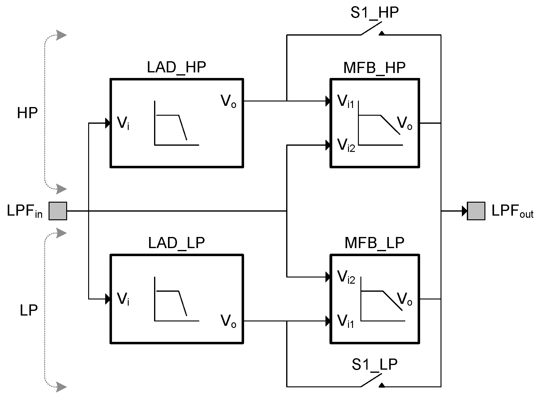
The structure of the proposed wideband reconfigurable integrated LPF for SDR transceivers is shown in Figure 2. Due to high requirements for bandwidth tuning range, the LPF is split into two paths—low frequency path (LP) and high frequency path (HP), where each path can be tuned over a decade. Moreover, this approach of split LPF paths gives several advantages to the design:
  • Optimization of the active stage. This feature allows optimizing layout size and power dissipation for each path, since size and current consumption of the LP active stage can be scaled in respect to HP, while maintaining same performance.
  • Compensation of each stage over the entire tuning range for each path can be optimized for large signal response.
  • Count of passive elements of the tuning banks in the LPF can be distributed in both paths, which reduces the size of the bandwidth control step over the entire LPF tuning range for the same bit count of the control word. Hence, size of the control step can be reduced without adding additional parasitic capacitance due to a large number of switching elements.
  • If the design requires, LP and HP can be split into two separate and independently controlled LPFs that can work with narrow and wide bandwidths simultaneously, for example in 5G NR NSA implementation.
The configuration of the order of the proposed LPF is achieved by designing both LP and HP paths with two independently controlled, interconnected filter stages—a 2nd and a 4th order implementation with a low-pass response. As shown in Figure 2, they are respectively designated as MFB_LP and LAD_LP for LP path, and MFB_HP and LAD_HP for HP path. Each path can be configured to either one of the stages or their combination. This allows each path to be configured as 2nd, 4th, or 6th order LPF.

Design of the Filter Stages

Active-RC topology is chosen for each stage of the filter, due to its high linearity and robustness with insensitivity to the parasitics compared to gm-C designs [18].
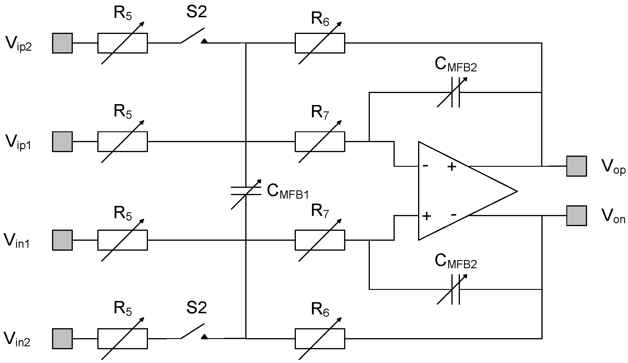
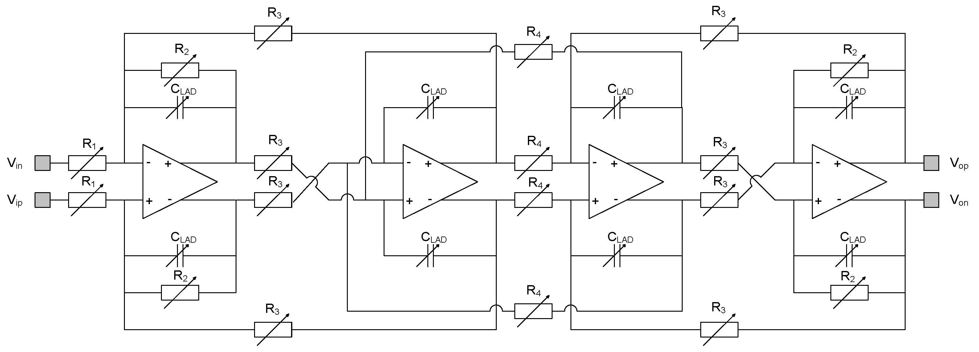
The 2nd and 4th order stages, respectively, use fully differential multiple feedback (MFB) topology and ladder filter (LAD) topologies. Their schematics are respectively shown in Figure 3 and Figure 4. Since MFB topology uses a single operational amplifier (OA), as opposed to two active stages in a biquad, it can be used for low power applications, while having excellent linearity performance. Ladder filter topology provides a more robust design for higher order filters against PVT.
MFB stage has two differential inputs Vip1, Vin1 and Vip2, Vin2. The first differential input is used when the active filter path is configured as a 6th order LPF, while the second differential input is used for 2nd order LPF configuration. This dual input approach removes the need to have two bypass transmission gates for each stage of the filter path—only the 2nd order stage is bypassed via a transmission gates under large signal conditions. These transmission gates in Figure 2 are marked as S1_LP and S1_HP for LP and HP paths, respectively. The S2 transmission gate in MFB topology (Figure 3) is placed at the summing node to achieve better linearity performance at large signal conditions.
Butterworth approximation is used for all stages in both LP and HP. Butterworth is chosen due to lower Q, which in turn relaxes OA gain–bandwidth product (GBWP) requirement. Furthermore, maximally flat passband response does not impact the signal-to-noise ratio (SNR) at large signal conditions, since minimal back off is not needed for margin against peaking in passband.
It can be noted that connecting a 2nd and 4th order filters of the proposed reconfigurable LPF in cascade produces a 6th order LPF transfer function (1), which is not equal to a 6th order Butterworth transfer function (2):
H ( s )   =   1 / ( ( s 2 +   s / 0.541   +   1 )   ×   ( s 2 +   s / 1.31   +   1 ) )   ×   1 / ( s 2 +   s / 0.707   +   1 ) ,
H ( s )   =   1 / ( ( s 2 +   s / 0.518   +   1 )   ×   ( s 2 +   s / 1.932   +   1 )   ×   ( s 2 +   s / 0.707   +   1 ) ) .
Cascading two filters with a Butterworth response retains the flatness in the passband, though if both 2nd and a 4th order filters have equal bandwidths, the overall path bandwidth will be reduced by ~14%, and have a slower roll-off around the transition band. Designing each stage with a higher maximum bandwidth limit can counter the aforementioned bandwidth reduction. Looking at (3), increase of the bandwidth limit for both 2nd and 4th order filters allows to relax the requirements by about 20% for OA GBWP for the same bandwidth, compared to implementing a 6th order Butterworth transfer function. The small change of the roll-off near the transition band can be easily corrected in the digital domain by a channel equalizer, which can be found in most wireless communication systems [26].
GBWP OA   2   ×   ω max ×   Q / Δ Q ,
where ωmax is the maximum passband frequency; Q is the maximum quality factor and ΔQ is the tolerable quality factor variation for the filter [22].
The requirement for OA GBWP can still be further reduced, if the bandwidth limit for the 2nd order filter is increased more than for the 4th order filter. In this scenario, the 2nd order filter would add additional signal suppression in stopband, while the 4th order filter would retain the near maximally flat response in the passband.

2.2. Calibration and Bandwidth Tuning

In the proposed filter structure, PVT induced variation and bandwidth tuning is implemented via digitally controlled resistor and capacitor tuning banks. Resistor banks are primarily used for IC process and temperature compensation, while capacitor banks are used to tune the bandwidth and to compensate for the residual, mostly constant, IC process parameter spread.

2.2.1. PVT Compensation

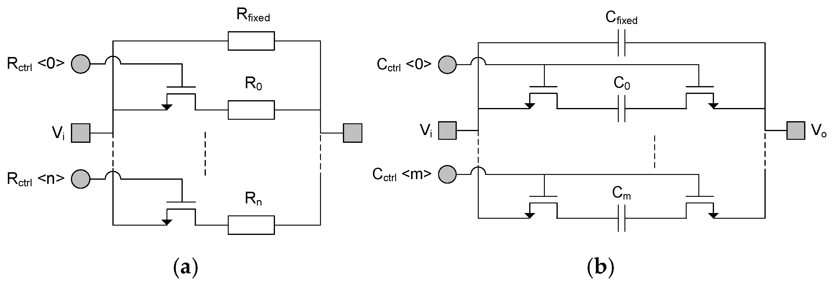
Resistor tuning banks in the 2nd and 4th order filters of both LP and HP paths use discrete–step tuning controls. They are composed of binary-controlled n number of MOS-switched resistors connected in parallel with a resistor of fixed value. The implementation of the resistor tuning bank with discrete control is shown in Figure 5a. The capacitor tuning bank utilizes the same structure, with a small modification for the CMFB1 bank (refer to Figure 3) of the 2nd order MFB filter, as shown in Figure 5b, where instead of one, two symmetrically placed MOS switches are used to equalize parasitic load on both summing nodes.
Careful selection of the quantity of the control bits for digital control of the resistor and capacitor tuning banks is important to minimize the total parasitic value from MOS switches. The value of the resistor Rfixed in the resistor tuning bank, as shown in (4), can be determined from the nominal value of the tuning bank R and the tuning range Δω, which is defined by the specific IC process and the desired margin. In this case, the minimum value of the resistance can be calculated from (5).
R fixed =   R   ×   ( 1   +   Δ ω / 100 % ) ,
R min =   R   ×   ( 1     Δ ω / 100 % ) ,
where Δω is the bandwidth tuning range expressed in percentage. The resistance, which is needed to change the value of the resistor tuning bank by a maximum tuning step size φR can then be found:
R p =   100 %   ×   ( R fixed ) 2 / ( R   ×   φ R )     R fixed ,
where φR is the maximum allowed tuning step size from the wanted frequency, expressed in percentage. The minimum number of MOS-switched resistors n needed to satisfy requirements of the tuning range Δω and tuning step size φR can be found using (7)–(9).
n = { α , α + 1 , β > 1 β 1 ,
α   = l o g 2 ( 2   ×   R fixed ×   Δ ω / ( R   ×   φ R ) ) ,
β   =   R min ×   ( R fixed ×   2 α +   R p ) / ( R fixed ×   R p ) ,
The values of the individual resistors in the tuning bank can then be found using (10).
R n =   R p / 2 n .
A resistor bank with step size of 7% and 5-bit control is used in the proposed filter, which has a tuning range of 42%. The tuning range is derived from the corner models of the 65 nm node process, where value spread of both resistors and capacitors are taken into account.

2.2.2. Bandwidth Tuning

Similarly, the minimum number of MOS-switched capacitors m, which is needed to meet the requirements of the tuning range for maximum and minimum bandwidth, with a desired maximum step φC can be calculated from (11).
m   = l o g 2 ( ω max / ω min ×   100 % / φ C )
where ωmax and ωmin are the maximum and minimum bandwidth, respectively, with bandwidth margins taken into account; φC is the maximum allowed step size from ωmax, expressed in percentage. The value of the smallest capacitor C0 can then be found as a ratio to Cfixed, using (12), while the values of the remaining capacitors are calculated in the same way as Rn using (10).
C fixed / C 0 =   ω min ×   ( 2 m 1 ) / ω min
For both proposed filter paths, the capacitor banks are designed with 8-bit control and Cfixed/C0 ratio of 22. The corresponding tuning ranges are 2.5–25 MHz and 20–200 MHz for the LP and HP path, respectively, with a 16% ωmax margin, and a 4.6% φC.

2.2.3. Calibration

The concept of calibration of the resistor tuning bank used for the LPF structure is shown in Figure 6. The calibration is done by comparing the value of an external temperature insensitive reference resistor Rext to the value of an internal resistor bank Rint. The internal resistor bank Rint is designed to have nominal value equal to Rext and same tuning specification as the resistor tuning bank in the LPF. Two internal stabilized current sources are used to create a voltage drop across both resistors, while a comparator is used to compare and tune the value of Rint.
Usually, direct transceiver architecture employs loopback-based direct channel calibration methods using a reference signal sweep to calibrate baseband induced imbalances, for example, amplitude and phase mismatches of the quadrature path signal [27]. Values of capacitors are much more stable over temperature compared to resistors, hence a single frequency sweep based on direct calibration can be used to determine the PVT-caused offset in the capacitor banks. Alternatively, dummy circuits can be added in the design to calibrate the value of the capacitor bank.

2.3. Operational Amplifier

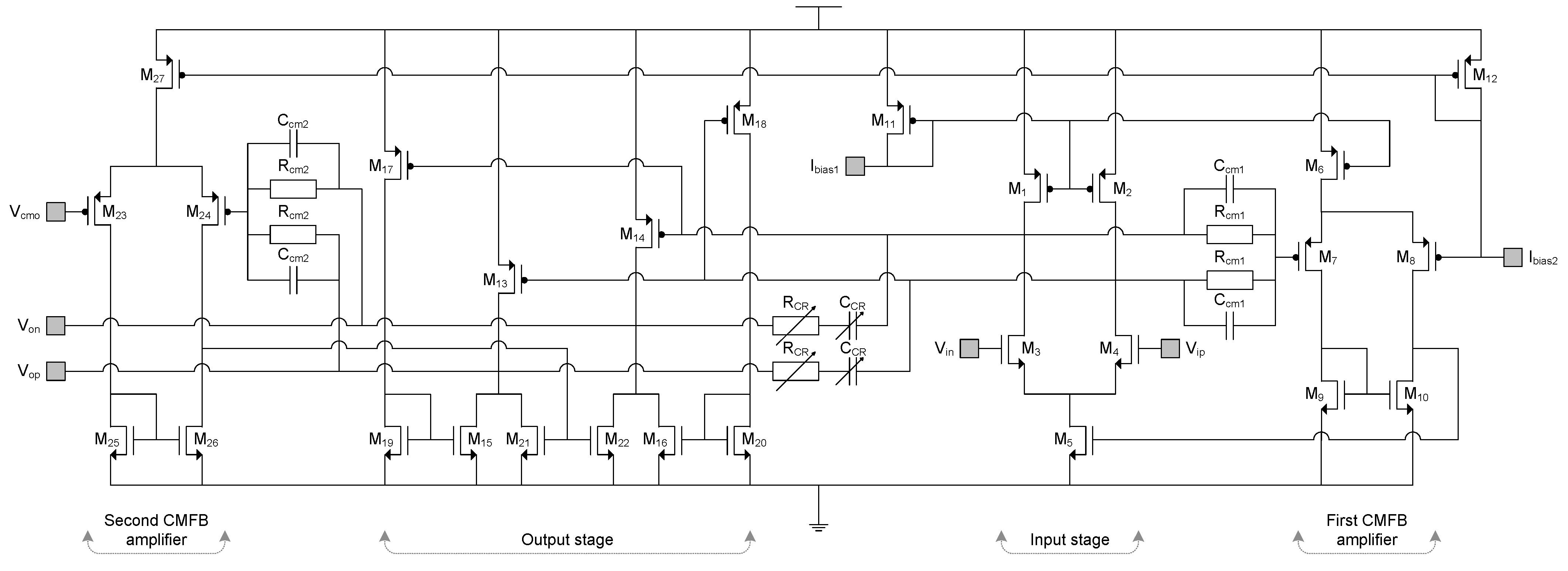
Linear active stages are critical for any high linearity filter, since they are the most contributing sources of nonlinearity [21]. The structure of two-stage fully differential operation amplifier (FDOA), used for both LPF topologies, is shown in Figure 7. The FDOA is composed of two gain stages, an input differential pair stage (M1–M5) and an output stage (M13–M22), both of which are controlled by two common mode feedback (CMFB) loop amplifiers. The biasing of the input stage and the first CMFB loop amplifier (M6–M10) can be controlled by changing the value of current source Ibias1, which is mirrored and scaled by M11. In a similar way, biasing of the output stage and second CMFB loop amplifier (M23–M27) can be controlled by Ibias2, which is mirrored and scaled by M12. The first CMFB loop amplifier controls the bias point of the output stage via M5.
The output stage is designed to work in class–A configuration, where each single-ended output leg is driven by the differential output of the input stage. The voltage of the common mode output of the FDOA is set by VCMO and controlled by the second CMFB loop amplifier via M21–M22 in the output stage. In the designed filter, the VCMO voltage is fixed to half of the supply voltage.
Passive RC common signal sense elements (Rcm1, Rcm2, Ccm1, Ccm2) are used between the input and output stage sensing nodes and the corresponding CMFB amplifier input for improved linearity performance, as opposed to using active elements. Miller compensation elements RCR and CCR are used between the input and output stages. The values of the resistor and capacitor are controlled using resistor and capacitor tuning banks, which have same structures as shown in Figure 5a. The corresponding control word of the LPF capacitor tuning bank is used to automatically select the required compensation values of the RCR and CCR.
When FDOA is powered down (circuitry is not show in Figure 7), the output stage is in a high-impedance state, where the impedance is mainly defined by the CMFB common signal sense and Miller compensation elements, if terminating switches are not present.
Control of Ibias1 and Ibias2 allows to change the GBWP of the FDOA at the expense of increased power consumption, without significantly affecting other FDOA parameters, such as gain and linearity. Thus, bias control enables power optimization of the FDOA at different filter bandwidth configurations, over a wide operation range.
LP and HP stages use same structure of the FDOA, but transistor sizing and driving strength are different to meet the different requirements for them. The FDOA in the 2nd and 4th order stages on the same path (LP or HP) are identical, only having subtle variations in the values of the RCR and CCR compensation bank.

3. Post-Layout Simulation Results

The proposed wideband reconfigurable integrated LPF was designed and verified using a 65-nm CMOS process. Layout of the designed filter in a quadrature baseband stage implementation is shown in Figure 8. The total occupied area for a single quadrature path is 0.429 mm2, where LP and HP path occupy 0.251 mm2 and 0.178 mm2, respectively. A single FDOA without Miller compensation elements occupies 0.0035 mm2 and 0.0058 mm2 in LP and HP path, respectively.

3.1. Operational Amplifier

In this section, results of post-layout simulation of the FDOA used in 2nd order filter are presented. Gain and phase response under nominal bias conditions of the LP and HP path FDOA is shown in Figure 9. The LP path FDOA has 43.1 dB gain, a phase margin of 50.8 degrees, and a bandwidth of 6.27 MHz, which equals a GBWP of 1.26 GHz. The power consumption is 2.32 mW from 1.2 V supply. Similarly, the HP path FDOA has 51.3 dB gain, a phase margin of 19.1 degrees, and a bandwidth of 7.59 MHz, which equals a GBWP of 2.22 GHz. The power consumption is 7.64 mW from 1.2 V supply.
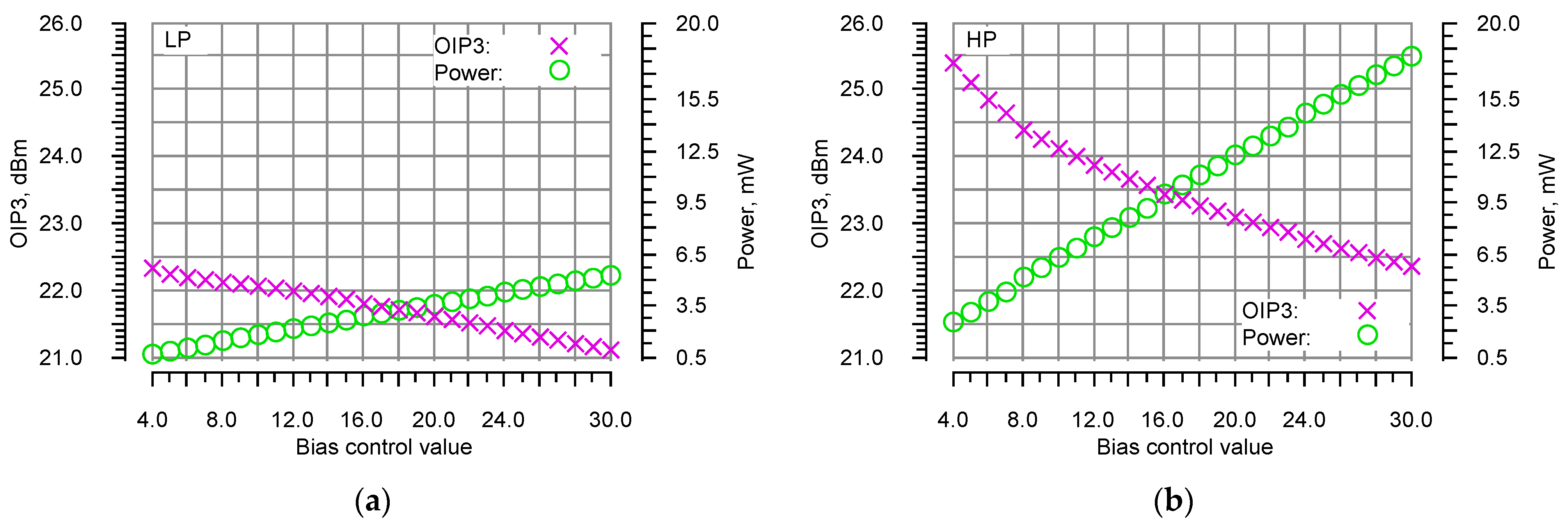
FDOA gain–bandwidth product, maximum passband gain, in-band output-referred third-order intercept point (OIP3) and power consumption at different bias control values are shown in Figure 10 and Figure 11. By changing the value of the bias control, power consumption can be used as a trade-off to change the GBWP of FDOA and optimize performance of the filter for different bandwidth settings. For LP and HP paths, respectively, the GBWP can be changed from 0.36 GHz to 2.7 GHz and from 0.85 GHz to 4.4 GHz. The change of bias has a small impact on other FDOA parameters. For LP path, the gain varies from 38 dB to 44.6 dB, the OIP3 from 22.4 dBm to 21.15 dBm, while for HP path, the gain varies from 49.8 dB to 51.3 dB, the OIP3 from 25.4 dBm to 22.4 dBm across the bias control range.

3.2. Low-Pass Filter

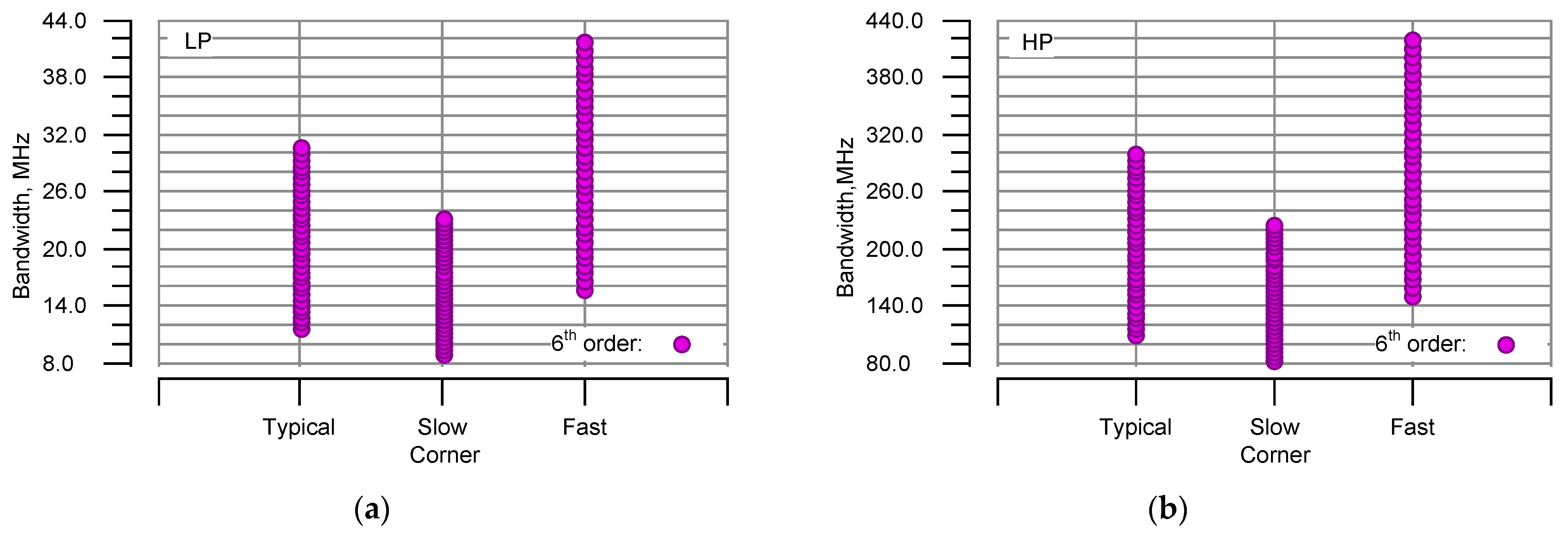
In this section, results of the post-layout simulation of the proposed wideband reconfigurable integrated LPF at different filter order and bandwidth configuration sets are presented. The tuning range of the resistor bank of the 6th order filter, a cascade of 2nd and 4th order filters, for both LP and HP can be seen in Figure 12. As seen from the overlapping bandwidth tuning ranges, resistor bank based frequency tuning is sufficient to compensate bandwidth offset related to technology process corner with a minimum tuning word margin of 5.
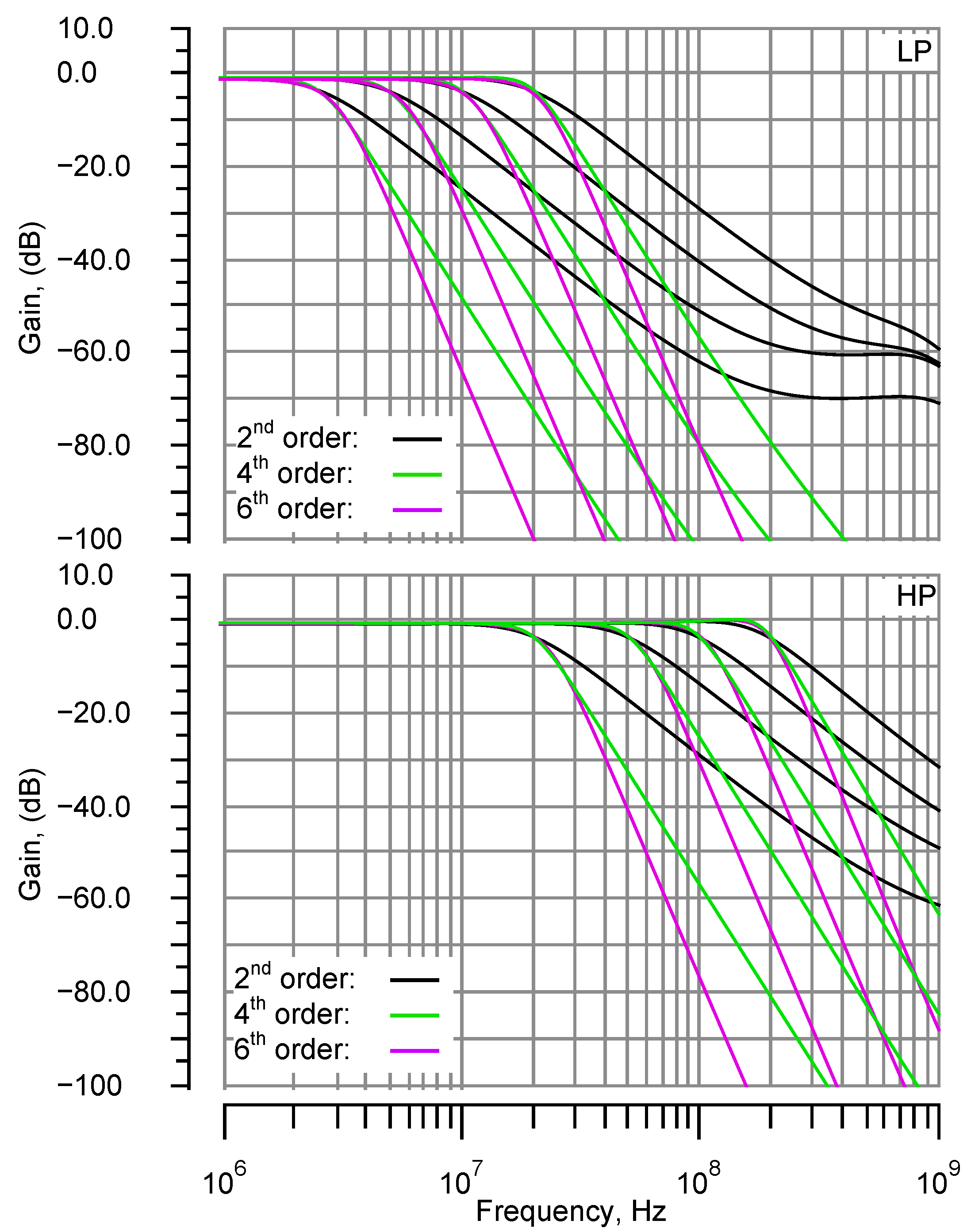
The filter response for all three configurations of the LPF order at various corner and intermediate bandwidth configurations is show in Figure 13. The gain varies from −0.55 dB to −0.84 dB with a maximum passband ripple of 0.1 dB for the LP across the entire bandwidth tuning range and for all configurations of the filter order. For the same HP configuration, the gain varies from −0.26 dB to −0.48 dB with a maximum passband ripple of 0.75 dB. The small negative gain is caused by resistor bank parameter variations in filter topologies, internal resistance of the transmission gates, and by finite gain of the FDOA. It is possible to compensate this by adding a separate control for either the R1 and R5 or the R3 and R4 pairs (see Figure 3 and Figure 4). Since margin of the tuning word is at least 5, an offset value for the selected pair can be added when tuning the bandwidth to compensate the gain variation of the LPF. Lastly it can be noted that the gain control in typical SDR transceivers is implemented by using VGA stages before or after the LPF.
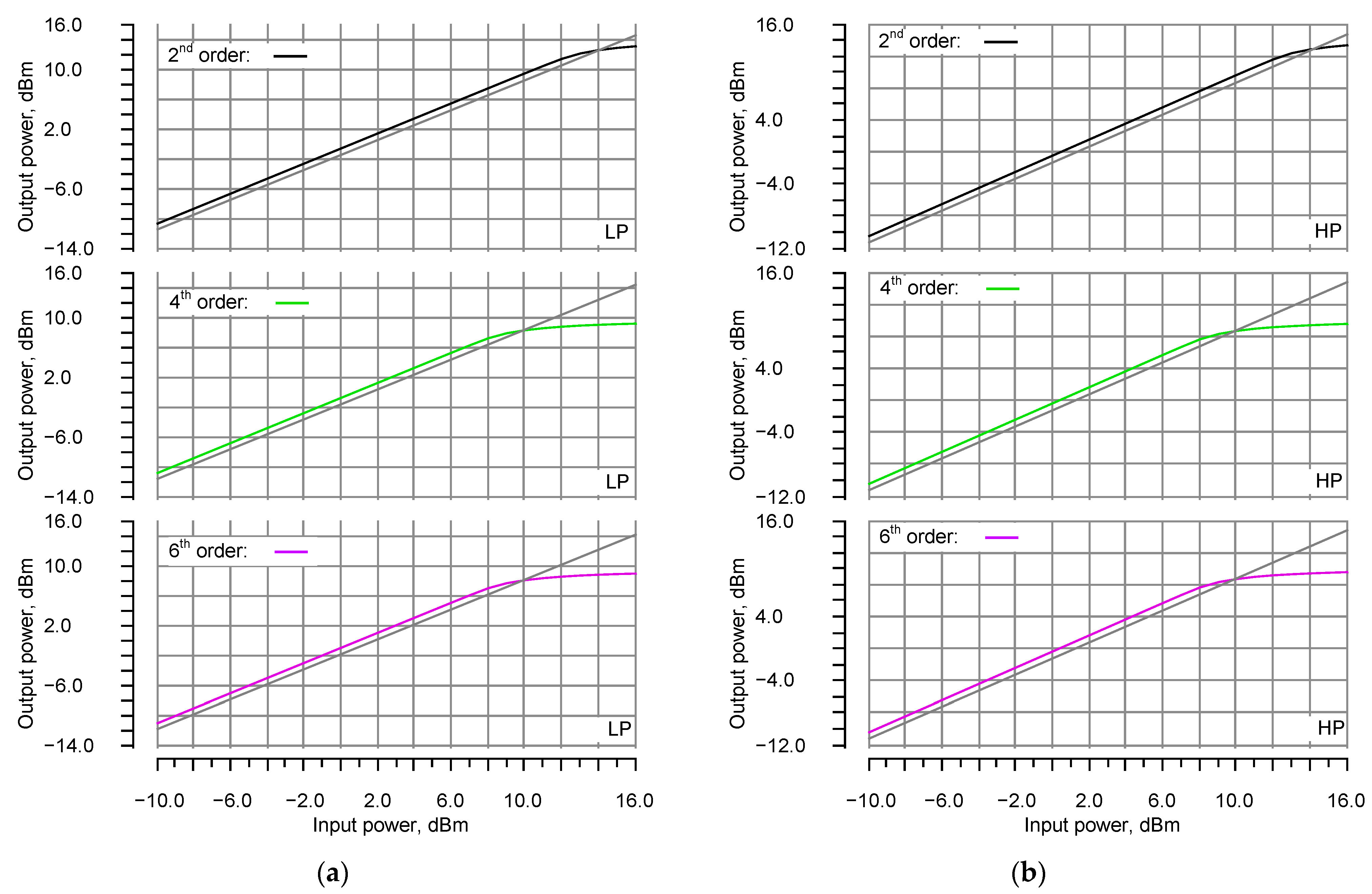
1 dB compression point (P1dB) for all three configurations of the filter order for LP and HP is shown in Figure 14. The 2nd order stage has a P1dB of 14.1 dBm, while the compression point of the 4th order stage is 9.9 dBm for both LP and HP. Due to cascaded structure of the 6th order configuration, its P1dB value is determined by the most nonlinear stage, and therefore it has the same value as the 4th order stage.
Since the capacitor bank are used in the filter for bandwidth selection and minimum bandwidth of the filter is well above the 1/f noise corner, LPF has small NF variation at same load conditions over the entire range of bandwidth control. Due to aforementioned small variations in NF and P1dB, large signal dynamic range per hertz of the proposed filter is nearly invariant to different sets of bandwidth and order configurations.
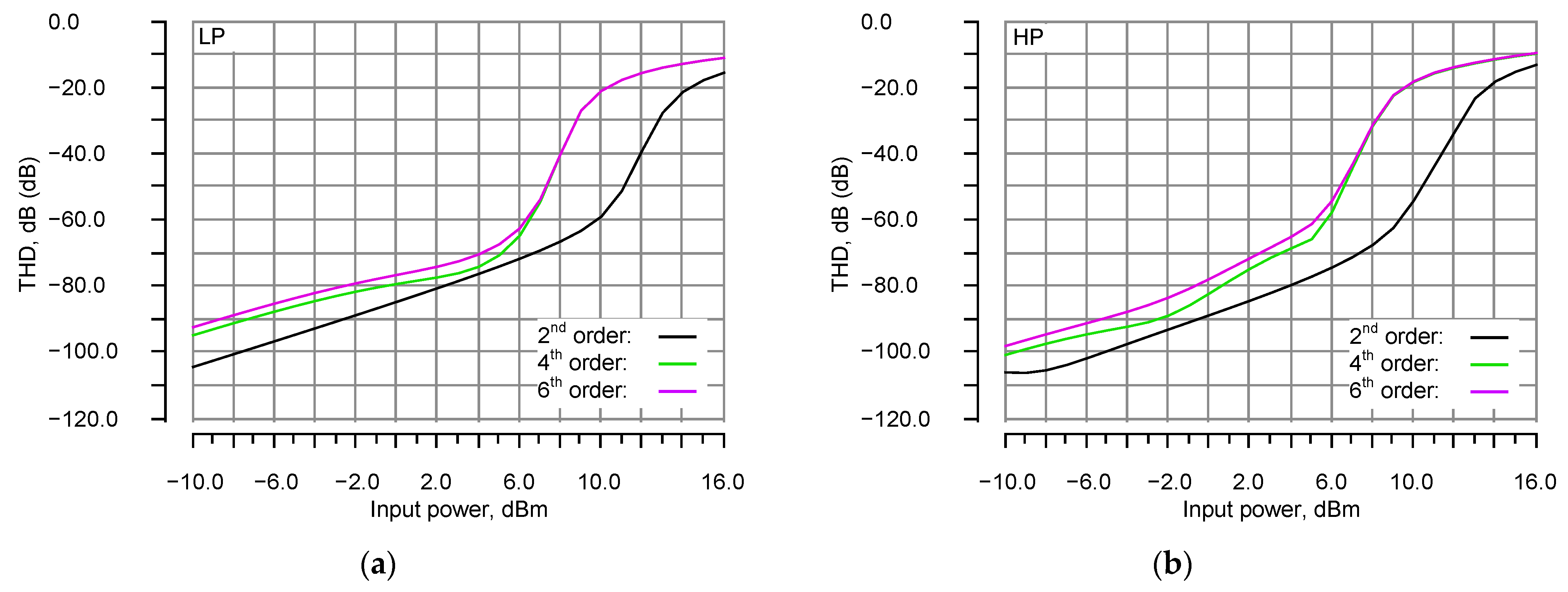
Total harmonic distortion (THD) for LP and HP is shown in Figure 15. If LP is configured for 20 MHz, THD values for 2nd, 4th and 6th filter order configuration vary from −103.1 dB to −91.7 dB with a 0.2 Vpp input and from −75.7 dB to −69.9 dB with a 1 Vpp input. One percentage THD is reached with 12 dBm for 2nd filter order and 8 dBm level input signal for 4th and 6th filter order.
When HP is configured for 200 MHz, values of the THD for the same configurations of the filter order vary from −105.5 dB to −97.4 dB with a 0.2 Vpp input and from −79.1 dB to −64.6 dB with a 1 Vpp input. One percentage THD is reached with 11.3 dBm for 2nd filter order and 7.2 dBm level input signal for 4th and 6th filter order.
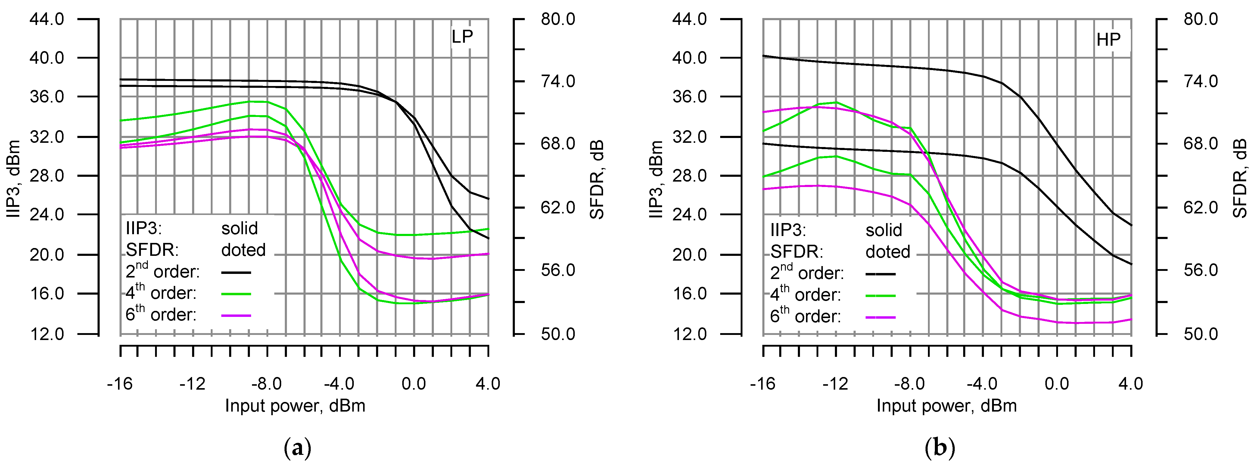
In-band input-referred third-order intercept point (IIP3) and spurious free dynamic range (SFDR) for LP and HP is shown in Figure 16. If LP is configured for 20 MHz, values of the IIP3 and SFDR for 2nd, 4th and 6th filter order configurations, respectively, vary from 32.7 dBm to 37.8 dBm and from 68.75 dB to 73.6 dB with 0.2 Vpp tones.
When HP is configured for 200 MHz, values of the IIP3 and SFDR for 2nd, 4th and 6th filter order configurations, respectively, vary from 34.2 dBm to 39.3 dBm and from 63.59 dB to 67.56 dB with 0.2 Vpp tones.
The results for key sets of LPF configuration are summarized in Table 1 and a comparison to previous works is presented in Table 2. Comparing the results, it can be seen, that the proposed filter has the best in-band IIP3 and THD parameters. Although the reported filter [20] has excellent NF and large signal distortion performance, it has to be noted that this is achieved by utilising input and output buffer stages with source and load matching. Comparing integrated noise and large signal dynamic performance (P1dB) of the proposed filter, it can be seen that it also has better parameters of the remaining lot.

4. Conclusions

In this work, a wideband reconfigurable integrated LPF for 5G NR compatible SDR solutions was designed and validated. The LPF has programmable bandwidth with 92.8 tuning ratio—from 2.5 MHz to 200 MHz. This is achieved by connecting two overlapping frequency paths that are connected in parallel, both using Active-RC topology. The order of the filter can be configured to realize a 2nd, 4th, or 6th order LPF function, it has built-in PVT compensation with a tuning range of ±42% and power management features, which enable optimization of the filter across its entire bandwidth tuning range.
The LPF was designed and verified using 65 nm CMOS process, it occupies 0.429 mm2 and uses a 1.2 V supply. Across the entire 2.5 MHz to 200 MHz bandwidth selection range of the LPF, in-band IIP3 varies between 32.7 dBm and 45.8 dBm. Similarly, THD value varies between −85.63 dB and −64.55 dB when amplitude of the input tone is 4 dBm. One percentage THD is reached when the level of the input signal is 11.3 dBm for 2nd filter order and 7.2 dBm for 4th and 6th filter orders. The large signal performance of the LPF is stable across its bandwidth tuning range—P1dB is equal to 14 dBm when the LPF is configured for 2nd order and 10 dBm when LPF implements a 4th and 6th order functions. Depending on the filter’s order and bandwidth configuration, power dissipation can vary between 1.2 mW and 73.4 mW. Power management and performance optimization is achieved by utilizing two biasing controls of the operational amplifier for different sets of filter configuration.
The best small signal linearity performance is achieved, when the LPF is configured for 2nd order multiple feedback topology, where in-band IIP3 and THD mean values across the entire range of bandwidth selection are respectively 39 dBm and −79 dB. Due to small variations in NF and P1dB, large signal dynamic range per hertz of the proposed filter is nearly invariant to different sets of bandwidth and order configurations.
As a future step, the designed LPF will be used as part of an analog baseband chain of SDR transceiver in both transmit and receive paths. The use cases for aforementioned SDR transceiver will be primarily targeted at Intelligent Transport Systems, which utilise a variety of different wireless standards, including 5G NR.

Author Contributions

Conceptualization, K.K.; investigation, K.K., M.J., and V.M.; resources, M.J.; writing—original draft preparation, K.K.; writing—review and editing, M.J., V.M., and R.N.; visualization, K.K., M.J., and V.M.; project administration, R.N.; funding acquisition, R.N. All authors have read and agreed to the published version of the manuscript.

Funding

This project has received funding from the European Regional Development Fund (project No 01.2.2-LMT-K-718-01-0054) under grant agreement with the Research Council of Lithuania (LMTLT).

Acknowledgments

The team of authors wishes to express their gratitude to European Regional Development Fund and the Research Council of Lithuania for financially supporting this research as a part of “Design and Research of Internet of Things (IoT) Framework Model and Tools for Intelligent Transport Systems” project, grant number DOTSUT-235, No. 01.2.2-LMT-K-718-01-0054.

Conflicts of Interest

The authors declare no conflict of interest.

References

  1. Selva, A.F.B.; Reis, A.L.G.; Lenzi, K.G.; Meloni, L.G.P.; Barbin, S.E. Introduction to the software-defined radio approach. IEEE Latin Am. Trans. 2012, 10, 1156–1161. [Google Scholar]
  2. Seth, S.; Kwon, D.H.; Venugopalan, S.; Son, S.W.; Zuo, Y.; Bhagavatula, V.; Lim, J.; Oh, D.; Cho, T.B. A Dynamically Biased Multiband 2G/3G/4G Cellular Transmitter in 28 nm CMOS. IEEE J. Solid-State Circuits 2016, 51. [Google Scholar] [CrossRef]
  3. Savić, M.; Božić, M.; Bukvić, B.; Grujić, D.N.; Tamosevicius, Z.; Kiela, K.; Back, A. 5G CrowdCell with mm-Wave SDR Based Backhaul. In Lecture Notes of the Institute for Computer Sciences, Social-Informatics and Telecommunications Engineering, LNICST; Springer: Cham, Switzerland, 2019; Volume 291. [Google Scholar]
  4. Kiela, K.; Barzdenas, V.; Jurgo, M.; Macaitis, V.; Rafanavicius, J.; Vasjanov, A.; Kladovscikov, L.; Navickas, R. Review of V2X-IoT standards and frameworks for ITS applications. Appl. Sci. 2020, 10, 4314. [Google Scholar] [CrossRef]
  5. Ishihara, N.; Amakawa, S.; Masu, K. RF CMOS integrated circuit: History, current status and future prospects. IEICE Trans. Fundam. Electron. Commun. Comput. Sci. 2011, 94, 556–567. [Google Scholar] [CrossRef]
  6. Xu, Z.; Zhou, J.; Yu, Z.; Huang, W.; Ni, Y.; Huang, F.; Chu, Y. Design of high performance RF transceiver for next generation wireless communications. In Proceedings of the 2012 International Conference on Microwave and Millimeter Wave Technology, ICMMT 2012, Shenzhen, China, 5–8 May 2012; Volume 1. [Google Scholar]
  7. Chakraborty, S.; Parikh, V.; Sankaran, S.; Motos, T.; Fikstvedt, O.; Marienborg, J.T.; Griffith, D.; Prathapan, I.; Nagaraj, K.; Zhang, F.; et al. An ultra low power, reconfigurable, multi-standard transceiver using fully digital PLL. In Proceedings of the IEEE Symposium on VLSI Circuits, Kyoto, Japan, 12–14 June 2013. [Google Scholar]
  8. Borremans, J.; Van Liempd, B.; Martens, E.; Cha, S.; Craninckx, J. A 0.9 V low-power 0.4–6 GHz linear SDR receiver in 28 nm CMOS. In Proceedings of the IEEE Symposium on VLSI Circuits, Kyoto, Japan, 12–14 June 2013. [Google Scholar]
  9. Kladovščikov, L.; Navickas, R.; Kiela, K. Self-tuning system for multistandard active RC filters. Microelectron. J. 2019, 90. [Google Scholar] [CrossRef]
  10. Han, D.O.; Kim, J.H.; Lee, K.D.; Park, S.G.; Oh, S.M.; Kim, E.J. Fully integrated dual-band transceiver for IEEE 802.11a/b/g/j/n wireless local area network applications with hybrid up/down conversion architecture. IET Circuits Devices Syst. 2011, 5. [Google Scholar] [CrossRef]
  11. Huang, Y.; Li, W.; Hu, S.; Xie, R.; Li, X.; Fu, J.; Sun, Y.; Pan, Y.; Chen, H.; Jiang, C.; et al. A high-linearity WCDMA/GSM reconfigurable transceiver in 0.13-μm CMOS. IEEE Trans. Microw. Theory Tech. 2013, 61. [Google Scholar] [CrossRef]
  12. Al-Yasir, Y.I.A.; Parchin, N.O.; Abd-Alhameed, R.A.; Abdulkhaleq, A.M.; Noras, J.M. Recent progress in the design of 4G/5G reconfigurable filters. Electronics 2019, 8, 114. [Google Scholar] [CrossRef] [Green Version]
  13. Baschirotto, A.; D’Amico, S.; De Matteis, M. Advances on analog filters for telecommunications. In Proceedings of the Advanced Signal Processing, Circuits, and System Design Techniques for Communications—2006 IEEE International Symposium on Circuits and Systems, ISCAS 2006, Kos, Greece, 21–24 May 2006. [Google Scholar]
  14. Khattak, M.K.; Lee, C.; Park, H.; Kahng, S. RF channel-selectivity sensing by a small antenna of metamaterial channel filters for 5G sub-6-GHz bands. Sensors 2020, 20, 1989. [Google Scholar] [CrossRef] [PubMed] [Green Version]
  15. Chih-Lin, I.; Kuklinski, S.; Chen, T.C.; Ladid, L.L. A perspective of O-RAN integration with MEC, SON, and network slicing in the 5G era. IEEE Netw. 2020, 34, 3–4. [Google Scholar]
  16. NR, Base Station (BS) Radio Transmission and Reception (Release 17), Tech. Specification Group Radio Access Network (TSG RAN), 3GPP TR 38.104. 2021. Available online: https://www.3gpp.org/ftp//Specs/archive/38_series/38.104/38104-h00.zip (accessed on 29 January 2021).
  17. Evolved Universal Terrestrial Radio Access (E-UTRA). Base Station (BS) Radio Transmission and Reception (Release 17), Tech. Specification Group Radio Access Network (TSG RAN), 3GPP TS 36.104. 2021. Available online: https://www.3gpp.org/ftp//Specs/archive/36_series/36.104/36104-h00.zip (accessed on 29 January 2021).
  18. Wang, Y.; Ye, L.; Liao, H.; Huang, R.; Wang, Y. Highly Reconfigurable Analog Baseband for Multistandard Wireless Receivers in 65-nm CMOS. IEEE Trans. Circuits Syst. II Express Briefs 2015, 62. [Google Scholar] [CrossRef]
  19. Lavalle-Aviles, F.; Sanchez-Sinencio, E. A 0.6-V Power-Efficient Active-RC Analog Low-Pass Filter with Cutoff Frequency Selection. IEEE Trans. Very Large Scale Integr. Syst. 2020, 28. [Google Scholar] [CrossRef]
  20. Lee, I.Y.; Im, D.; Ko, J.; Lee, S.G. A 50-450 MHz Tunable RF Biquad Filter Based on a Wideband Source Follower With > 26 dBm IIP3, +12 dBm P1dB, and 15 dB Noise Figure. IEEE J. Solid-State Circuits 2015, 50. [Google Scholar] [CrossRef]
  21. Wu, W.; Mo, T.; Lu, Z. A 180 nm CMOS three stage feedforward compensation op-amp with linearity improvement technique for active RC LPF. In Proceedings of the 2016 10th IEEE International Conference on Anti-Counterfeiting, Security, and Identification (ASID), Xiamen, China, 23–25 September 2016. [Google Scholar]
  22. Wu, B.; Chiu, Y. A 40 nm CMOS derivative-free if Active-RC BPF with programmable bandwidth and center frequency achieving over 30 dBm IIP3. IEEE J. Solid-State Circuits 2015, 50. [Google Scholar] [CrossRef]
  23. D’Amico, S.; Baschirotto, A.; Philips, K.; Rousseaux, O.; Gyselinckx, B. A 240 MHz Programmable Gain Amplifier & filter for ultra low power low-rate UWB receivers. In Proceedings of the ESSCIRC 2009—35th European Solid-State Circuits Conference, Athens, Greece, 14–18 September 2009. [Google Scholar]
  24. Fary, F.; Mangiagalli, L.; Vallicelli, E.; De Matteis, M.; Baschirotto, A. A 28 nm bulk-CMOS 50 MHz 18 dBm-IIP3 Active-RC Analog Filter based on 7 GHz UGB OTA. In Proceedings of the ESSCIRC 2019—IEEE 45th European Solid State Circuits Conference, Cracow, Poland, 23–26 September 2019. [Google Scholar]
  25. Yen, M.Y.; Chen, H.C.; Wei, Y.L.; Chung, C.Y. A CMOS transmitter analog baseband for 5G mobile communication. Electronics 2019, 8, 1319. [Google Scholar] [CrossRef] [Green Version]
  26. Wang, H.F.; Hwang, C.P.; Chen, M.S. The Error Vector Magnitude (EVM) performance in LTE Downlink. In Proceedings of the 2019 Cross Strait Quad-Regional Radio Science and Wireless Technology Conference, CSQRWC 2019, Taiyuan, China, 18–21 July 2019. [Google Scholar]
  27. Aoki, Y.; Dao, M.T.; Min, K.; Hwang, Y.; Kim, Y.; Yang, S.G. 1.4-GHz Bandwidth Frequency-Dependent I/Q Imbalance Calibration for 5G mmWave Communications. In Proceedings of the IEEE MTT-S International Microwave Symposium, Boston, MA, USA, 2–7 June 2019. [Google Scholar]
  28. De Matteis, M.; Pipino, A.; Resta, F.; Pezzotta, A.; D’Amico, S.; Baschirotto, A. A 63-dB DR 22.5-MHz 21.5-dBm IIP3 Fourth-Order FLFB Analog Filter. IEEE J. Solid-State Circuits 2017, 52. [Google Scholar] [CrossRef]
Figure 1. General structure diagram of a direct conversion architecture transceiver.
Electronics 10 00734 g001
Figure 2. Structure of the proposed wideband reconfigurable integrated low-pass filter.
Electronics 10 00734 g002
Figure 3. Schematic of 2nd order active-RC multiple feedback topology low-pass filter.
Electronics 10 00734 g003
Figure 4. Schematic of 4th order active-RC ladder topology low-pass filter.
Electronics 10 00734 g004
Figure 5. Schematic of: (a) resistor tuning bank with discrete control; (b) capacitor tuning bank with discrete control.
Electronics 10 00734 g005
Figure 6. Structure of the resistor bank calibration.
Electronics 10 00734 g006
Figure 7. Schematic of the proposed fully differential operational amplifier for 2nd and 4th order low-pass filter topologies.
Electronics 10 00734 g007
Figure 8. Layout of the wideband reconfigurable integrated low-pass filter in quadrature baseband configuration.
Electronics 10 00734 g008
Figure 9. Gain and phase response under nominal bias conditions of the fully differential operational amplifiers used in 2nd order filter: (a) low frequency path (LP); (b) high frequency path (HP).
Electronics 10 00734 g009
Figure 10. Gain–bandwidth product (GBWP) and maximum gain response at different bias control values of the fully differential operational amplifiers used in 2nd order filter: (a) low frequency path (LP); (b) high frequency path (HP).
Electronics 10 00734 g010
Figure 11. In-band output-referred third-order intercept point (OIP3) and power consumption at different bias control values of the fully differential operational amplifiers used in 2nd order: (a) low frequency path (LP); (b) high frequency path (HP). OIP3 input tone configuration: 1 MHz and 1.7 MHz, both tone amplitude −10 dBm.
Electronics 10 00734 g011
Figure 12. Bandwidth tuning range at different technology process corners for the 6th order configuration: (a) low frequency path (LP), configured for 20 MHz bandwidth; (b) high frequency path (HP), configured for 200 MHz bandwidth.
Electronics 10 00734 g012
Figure 13. Low frequency path (LP) and high frequency path (HP) response for all order configurations, tuned to 2.5 MHz, 5 MHz, 10 MHz, 20 MHz, 50 MHz, 100 MHz, and 200 MHz.
Electronics 10 00734 g013
Figure 14. 1 dB compression point (P1dB) for all filter order configurations: (a) low frequency path (LP), configured for 20 MHz bandwidth; (b) high frequency path (HP), configured for 200 MHz bandwidth. Input tone frequency: 10% of bandwidth.
Electronics 10 00734 g014
Figure 15. Total harmonic distortion (THD) at different input power levels for all filter order configurations: (a) low frequency path (LP), configured for 20 MHz bandwidth; (b) high frequency path (HP), configured for 200 MHz bandwidth. Input tone frequency: 10% of bandwidth.
Electronics 10 00734 g015
Figure 16. In-band input-referred third-order intercept point (IIP3) and spurious free dynamic range (SFDR) at different input power levels for all filter order configurations: (a) low frequency path (LP), configured for 20 MHz bandwidth; (b) high frequency path (HP), configured for 200 MHz bandwidth. IIP3 input tone configuration: first at 40%, second at 70% of bandwidth, both tone amplitude −10 dBm.
Electronics 10 00734 g016
Table 1. Summary of the designed wideband reconfigurable integrated low-pass filter parameters.
PathLow Frequency Path (LP)How Frequency Path (HP)
Technology65 nm CMOS
Supply, V1.2
Tuning ratio92.8
11.611.6
Topology 1 Active-RC
MFBLADMFB + LADMFBLADMFB + LAD
Type 2LPF-BLPF-BLPF-C-BLPF-BLPF-BLPF-C-B
Order2nd 4th6th2nd 4th6th
Area, mm20.0730.1720.2510.0440.1310.178
Gain, dB−0.55−0.57−0.84−0.48−0.26−0.39
P1dB, dBm14.069.959.9414.29.949.94
Bandwidth, MHz2.5202.5202.520202002020020200
In-band IIP3, dBm 338.8438.5836.3235.5135.0534.8345.8144.6137.6137.9436.0336.72
38.4837.7935.0133.8533.3132.6641.9339.3436.7933.7738.4234.16
Out-band IIP3, dBm 438.9436.9828.1924.3225.6622.1735.7237.3732.5720.6630.2116.06
SFDR, dB 379.4574.1378.4673.0475.4770.279.3271.0775.1268.5771.5265.29
79.2173.677.5871.9474.3168.7576.7367.5674.5865.7673.1263.59
THD, dB 5−105−103.7−95.1−94.16−92.3−91.74−112.4−105.5−104.4−100.1−101.2−97.39
−76.95−75.7−74.75−73.57−72.11−69.85−85.63−79.06−71.64−68.04−69.22−64.55
NF, dB29.6528.3428.6226.931.8330.4827.7828.9525.8726.0529.729.74
Intg. Noise, µVRMS 621.8852.819.8245.3128.4567.7249.43182.240.19132.362.13202.7
Noise Floor, dBm−80.35−72.63−78.17−70.48−78.17−70.48 −73.19−62.02−75.08−64.92−71.26−61.23
Dynamic range, dB 794.2686.5491.1883.8787.9680.2887.2476.0784.8974.7181.0671.02
92.284.4889.2381.9286.0278.3484.3473.1782.1571.9778.3568.28
Dynamic range, dB-Hz 8158.24159.55155.16156.88151.94153.29160.25159.08157.9157.72154.07154.03
Power, mW1.192.314.989.56.211.83.914.815.958.619.873.4
1 MFB—multiple feedback topology; LAD—ladder topology. 2 LPF-B—Butterworth; LPF-C-B—cascaded Butterworth. 3 Upper numbers with input tone configuration: first at 10%, second at 19% of bandwidth, both tone amplitude −10 dBm; lower numbers with input tone configuration: first at 40%, second at 70% of bandwidth, both tone amplitude −10 dBm. 4 Input tone configuration: first at 150%, second at 250% of bandwidth, both tone amplitude −10 dBm. 5 Upper numbers with −10 dBm input tone; lower numbers with 4 dBm input tone. 6 Integrated from 1 kHz to Bandwidth. 7 Upper numbers at P1dB value; lower numbers at 1% THD value. 8 P1dB/(k × T × Noise Factor) [22].
Table 2. Summary of the designed wideband reconfigurable integrated low-pass filter parameters.
[19] 3[24] 4[20] 5[28] 6This Work 7
Process130 nm CMOS28 nm CMOS180 nm CMOS180 nm CMOS65 nm CMOS
Supply, V0.61.11.81.81.2
Tuning ratio4N/A9N/A92.8
Topology 1 A-RCgm-CA-RCA-RC/A-gm-RCA-RC
C-BQ-SK-BQFLFBMFB + LAD
Type 2LPF-BLPF-BLPFLPF-BLPF-C-B
Order4th 6th 246th
Bandwidth, MHz20–1605050–45022.52.5200
Area, mm20.2360.20.50.350.429
Gain, dB0−5.800.5−0.84−0.39
P1dB, dBm6.96–4.262.8, 4.5128.59.949.94
In-band IIP3, dBm21–9.5618, 16.527–2421.5, 935.0536.72
Out-band IIP3, dBm17.4–9.7---25.6616.06
SFDR, dB66.6–50.7−42.5--75.4765.29
THD, dB66.2–50.7−40-−40, −30−72.11−64.55
NF, dB--15-31.8329.74
Intg. Noise, µVRMS243–520277-8728.45202.7
Dynamic range, dB64.2–51-93.84–84.306386.0268.28
Power, mW5.56–23.773.6325.212.66.273.4
1 A-RC—active RF; C-BQ—cascaded biquad; SK-BQ—Sallen-Key biquad; FLFB—follow-the-leader-feedback; MFB—multiple feedback topology; LAD—ladder topology. 2 BPF-CH—bandpass filter, Chebyshev; LPF-B—Butterworth; LPF-C-B—cascaded Butterworth. 3 In-band IIP3 frequencies for 20 MHz were 6 MHz and 7 MHz, for 160 MHz–48 MHz and 56 MHz; Intg. Noise integrated from 1 to Bandwidth; Dynamic range at 1% THD. 4 P1dB, at 10 MHz and 40 MHz; In-band IIP3 frequencies 10 MHz and 11 MHz, 40 MHz and 41 MHz; SFDR is in dBc, with 40 MHz and 41 MHz, −5 dBm input tones; THD is in dBc, with an input tone 10 MHz, 1 dBm, includes up to 5th harmonics. 5 Uses Low noise amplifier—Source Follower—LPF—Output buffer configuration. Designed with 50Ω resistor banks, therefore low NF value at expense of area and power. In-band IIP3 frequencies 40 MHz and 50 MHz, 290 MHz and 300 MHz at 50 MHz and 300 MHz, −4 dBm input tones. 6 P1dB, at 5 MHz; In-band IIP3 frequencies 5 MHz and 6 MHz, 20 MHz and 21 MHz; THD is in dBc, input tone 2 MHz and 10 MHz, 0.33 V0-Peak. 7 See Table 1 for conditions.
Publisher’s Note: MDPI stays neutral with regard to jurisdictional claims in published maps and institutional affiliations.