
Study and Assessment of Defect and Trap Effects on the Current Capabilities of a 4H-SiC-Based Power MOSFET


 ,
,  and
and
Abstract
1. Introduction
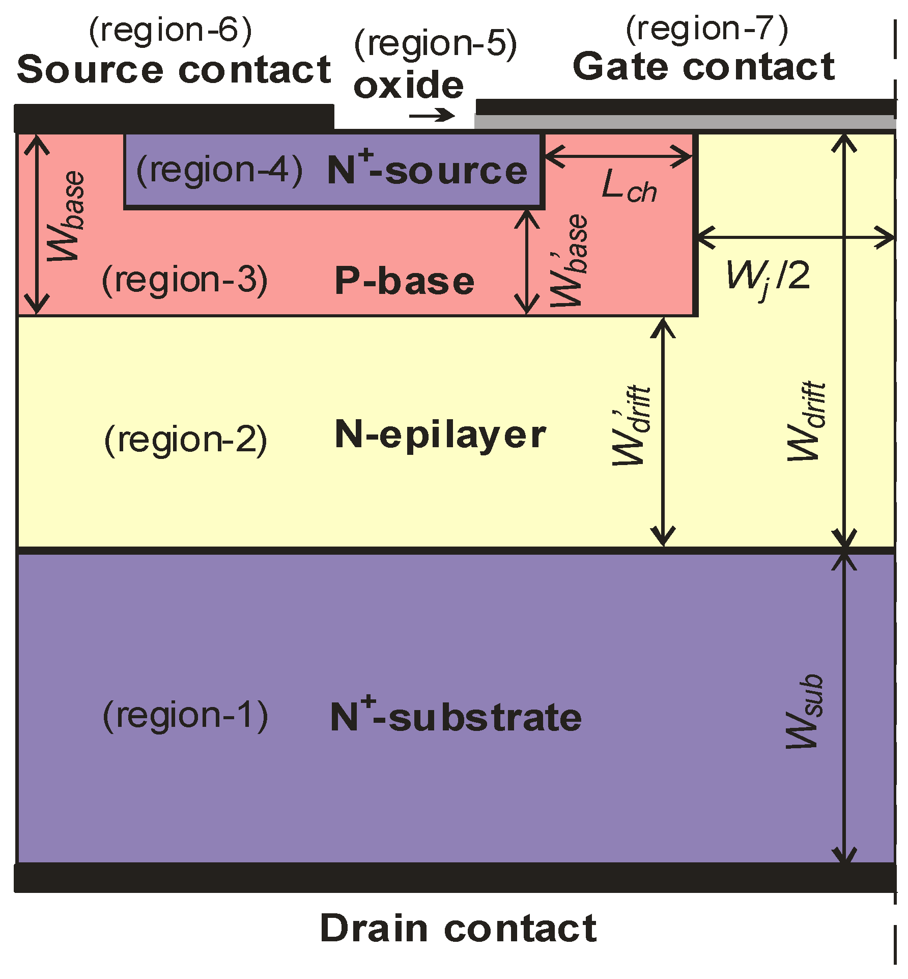
2. Device Structure
3. Physical Models
3.1. H-SiC/SiO2 Interface Traps
3.2. H-SiC Intrinsic Defects
4. Results and Discussion
5. Conclusions
Author Contributions
Funding
Conflicts of Interest
References
- Baliga, B.J. Silicon Carbide Power Devices; World Scientific: Singapore, 2005. [Google Scholar]
- SiC MOSFETs. Available online: https://www.rohm.com/products/sic-power-devices/sic-mosfet.
- Discrete SiC MOSFETs. Available online: https://www.wolfspeed.com/power/products/sic-mosfets.
- Silicon Carbide CoolSiC™ MOSFETs. Available online: https://www.infineon.com/cms/en/product/power/mosfet/silicon-carbide/.
- Tachiki, H.; Ono, T.; Kobayashi, T.; Tanaka, H.; Kimoto, T. Estimation of threshold voltage in SiC short-channel MOSFETs. IEEE Trans. Electron. Dev. 2018, 65, 3077–3080. [Google Scholar] [CrossRef]
- Tanimoto, Y.; Saito, A.; Matsuura, K.; Kikuchihara, H.; Mattausch, H.J.; Miura-Mattausch, M.; Kawamoto, N. Power-loss prediction of high-voltage SiC-mosfet circuits with compact model including carrier-trap influences. IEEE Trans. Power Electron. 2016, 31, 4509–4516. [Google Scholar] [CrossRef]
- Ettisserry, D.P.; Goldsman, N.; Lelis, A. A methodology to identify and quantify mobility-reducing defects in 4H-silicon carbide power metal-oxide-semiconductor field-effect transistors. J. Appl. Phys. 2014, 115, 103706. [Google Scholar] [CrossRef]
- Haasmann, D.; Dimitrijev, S. Energy position of the active near-interface traps in metal-oxide-semiconductor field-effect transistors on 4H-Sic. Appl. Phys. Lett. 2013, 103, 1135061–1135063. [Google Scholar] [CrossRef]
- Hornos, T.; Gali, A.; Svensson, B.G. Negative-U system of carbon vacancy in 4H-SiC. Mater. Sci. Forum 2011, 679, 261–264. [Google Scholar] [CrossRef]
- Danno, K.; Nakamura, D.; Kimoto, T. Investigation of carrier lifetime in 4H-SiC epilayers and lifetime control by electron irradiation. Appl. Phys. Lett. 2007, 90, 202109. [Google Scholar] [CrossRef]
- Kawahara, K.; Trinh, X.T.; Son, N.T.; Janzen, E.; Suda, J.; Kimoto, T. Quantitative comparison between Z1/2 center and carbon vacancy in 4H-SiC. J. Appl. Phys. 2014, 115, 143705. [Google Scholar] [CrossRef]
- Booker, I.D.; Janzén, E.; Son, N.T.; Hassan, J.; Stenberg, P.; Sveinbjörnsson, E.Ö. Donor and double-donor transitions of the carbon vacancy related EH6∕7 deep level in 4H-SiC. J. Appl. Phys. 2016, 119, 235703. [Google Scholar] [CrossRef]
- Della Corte, F.G.; De Martino, G.; Pezzimenti, F.; Adinolfi, G.; Graditi, G. Numerical simulation study of a low breakdown voltage 4H-SiC MOSFET for photovoltaic module-level applications. IEEE Trans. Electron. Devices 2018, 65, 3352–3360. [Google Scholar] [CrossRef]
- Bencherif, H.; Dehimi, L.; Pezzimenti, F.; De Martino, G.; Della Corte, F.G. Multiobjective optimization of design of 4H-SiC power MOSFETs for specific applications. J. Electron. Mater. 2019, 48, 3871–3880. [Google Scholar] [CrossRef]
- De Martino, G.; Pezzimenti, F.; Della Corte, F.G. Interface trap effects in the design of a 4H-SiC MOSFET for low voltage applications. In Proceedings of the 2018 International Semiconductor Conference (CAS), Sinaia, Romania, 10–12 October 2018. [Google Scholar]
- Bencherif, H.; Pezzimenti, F.; Dehimi, L.; Della Corte, F. Analysis of 4H-SiC MOSFET with distinct high-k/4H-SiC interfaces under high temperature and carrier-trapping conditions. Appl. Phys. A-Mater. 2020, 126, 854. [Google Scholar] [CrossRef]
- Bencherif, H.; Dehimi, L.; Athamena, N.E.; Pezzimenti, F.; Megherbi, M.L.; Della Corte, F.G. Simulation Study of Carbon Vacancy Trapping Effect on Low Power 4H-SiC MOSFET Performance. Silicon 2021, 1–9. [Google Scholar] [CrossRef]
- Silvaco Int. Atlas User’s Manual, Device Simulator Software. Available online: https://www.eng.buffalo.edu/~wie/silvaco/atlas_user_manual.pdf (accessed on 2 October 2004).
- Okamoto, M.; Iijima, M.; Nagano, T.; Fukuda, K.; Okumura, H. Controlling characteristics of 4H-SiC (0001) p-channel MOSFETs fabricated on ion-implanted n-well. Mater. Sci. Forum 2012, 717, 781–784. [Google Scholar] [CrossRef]
- Sung, W.; Baliga, B.J. Monolithically integrated 4H-SiC MOSFET and JBS diode (JBSFET) using a single Ohmic/Schottky process scheme. IEEE Electron. Device Lett. 2016, 37, 1605–1608. [Google Scholar] [CrossRef]
- Mikamura, Y.; Hiratsuka, K.; Tsuno, T.; Michikoshi, H.; Tanaka, S.; Masuda, T.; Sekiguchi, T. Novel designed SiC devices for high power and high efficiency systems. IEEE Trans. Electron. Devices 2014, 62, 382–389. [Google Scholar] [CrossRef]
- Baliga, B.J. Fundamentals of Power Semiconductor Devices; Springer: New York, NY, USA, 2008. [Google Scholar]
- Harada, S.; Okamoto, M.; Yatsuo, T.; Adachi, K.; Fukuda, K.; Arai, K. 8.5-mΩ·cm2 600-V Double-Epitaxial MOSFETs in 4H–SiC. IEEE Electron. Device Lett. 2004, 25, 292–294. [Google Scholar] [CrossRef]
- Selberherr, S. Analysis and Simulation of Semiconductor Devices; Springer: New York, NY, USA, 1984. [Google Scholar]
- Li, X.; Luo, Y.; Fursin, L.; Zhao, J.H.; Pan, M.; Alexandrov, P.; Weiner, M. On the temperature coefficient of 4H-SiC BJT current gain. Solid State Electron. 2003, 47, 233–239. [Google Scholar] [CrossRef]
- Ruff, M.; Mitlehner, H.; Helbig, R. SiC devices physics and numerical simulation. IEEE Trans. Electron. Devices 1994, 41, 1040–1054. [Google Scholar] [CrossRef]
- Lindefelt, U. Doping-induced band edge displacements and band gap narrowing in 3C-, 4H-, 6H-SiC, and Si. J. Appl. Phys. 1998, 84, 2628–2637. [Google Scholar] [CrossRef]
- Landsberg, P.T.; Kousik, G.S. The connection between carrier lifetime and doping density in nondegenerate semiconductors. J. Appl. Phys. 1984, 56, 1696–1700. [Google Scholar] [CrossRef]
- Roschke, M.; Schwierz, F. Electron mobility models for 4H, 6H, and 3C SiC. IEEE Trans. Electron. Devices 2001, 48, 1442–1447. [Google Scholar] [CrossRef]
- Raghunathan, R.; Baliga, B.J. Measurement of electron and hole impact ionization coefficients for SiC. In Proceedings of the 9th International Symposium on Power Semiconductor Devices and IC’s, Weimar, Germany, 26–29 May 1997. [Google Scholar]
- Pezzimenti, F.; Bencherif, H.; Yousfi, A.; Dehimi, L. Current-voltage analytical model and multiobjective optimization of design of a short channel gate-all-around-junctionless MOSFET. Solid State Electron. 2019, 161, 107642. [Google Scholar] [CrossRef]
- Galeckas, A.; Linnros, J.; Grivickas, V.; Lindefelf, U.; Hallin, C. Auger recombination in 4H-SiC: Unusual temperature behaviour. Appl. Phys. Lett. 1997, 71, 3269–3271. [Google Scholar] [CrossRef]
- Zeghdar, K.; Bencherif, H.; Dehimi, L.; Pezzimenti, F.; Della Corte, F.G. Simulation and analysis of the forward bias current–voltage–temperature characteristics of W/4H-SiC Schottky barrier diodes for temperature-sensing applications. Solid State Electron. Lett. 2020, 2, 49–54. [Google Scholar] [CrossRef]
- Pezzimenti, F. Modeling of the steady state and switching characteristics of a normally-off 4H-SiC trench bipolar-mode FET. IEEE Trans. Electron. Devices. 2013, 60, 1404–1411. [Google Scholar] [CrossRef]
- Megherbi, M.L.; Pezzimenti, F.; Dehimi, L.; Saadoune, A.; Della Corte, F.G. Analysis of the forward I-V characteristics of Al-implanted 4H-SiC p-i-n diodes with modeling of recombination and trapping effects due to intrinsic and doping-induced defect states. J. Electron. Mater. 2018, 47, 1414–1420. [Google Scholar] [CrossRef]
- Pezzimenti, F.; Della Corte, F.G. Design and modeling of a novel 4H-SiC normally-off BMFET transistor for power applications. In Proceedings of the Melecon 2010–2010 15th IEEE Mediterranean Electrotechnical Conference, Valletta, Malta, 26–28 April 2010. [Google Scholar]
- Megherbi, M.L.; Pezzimenti, F.; Dehimi, L.; Rao, S.; Della Corte, F.G. Analysis of different forward current—Voltage behaviours of Al implanted 4H-SiC vertical p–i–n diodes. Solid State Electron. 2015, 109, 12–16. [Google Scholar] [CrossRef]
- Zeghdar, K.; Dehimi, L.; Pezzimenti, F.; Megherbi, M.L.; Della Corte, F.G. Analysis of the electrical characteristics of Mo/4H-SiC Schottky barrier diodes for temperature-sensing applications. J. Electron. Mater. 2020, 49, 1322–1329. [Google Scholar] [CrossRef]
- Sharma, P.; Minakshi, M.; Watcharatharapong, T.; Laird, D.; Euchner, H.; Ahuja, R. Zn Metal Atom Doping on the Surface Plane of One-Dimesional NiMoO4 Nanorods with Improved Redox Chemistry. ACS Appl. Mater. Interfaces 2020, 12, 44815–44829. [Google Scholar] [CrossRef]
- Sharma, P.; Minakshi, M.; Singh, D.; Ahuja, R. Highly Energetic and Stable Gadolinium/Bismuth Molybdate with a Fast Reactive Species, Redox Mechanism of Aqueous Electrolyte. ACS Appl. Energy Mater. 2020, 3, 12385–12399. [Google Scholar] [CrossRef]
- Dhar, S.; Haney, S.; Cheng, L.; Ryu, S.R.; Agarwal, A.K. Inversion layer carrier concentration and mobility in 4H-SiC metal-oxide-semiconductor field-effect transistors. J. Appl. Phys. 2010, 108, 054509. [Google Scholar] [CrossRef]
- Potbhare, S.; Goldsman, N.; Pennington, G. Numerical and experimental characterization of 4H-silicon carbide lateral metal-oxide-semiconductor field-effect transistors. J. Appl. Phys. 2006, 100, 044515. [Google Scholar] [CrossRef]
- Potbhare, S.; Goldsman, N.; Lelis, A.; McGarrity, J.M.; McLean, F.B. A physical model of high temperature 4H-SiC MOSFETs. IEEE Trans. Electron. Devices 2008, 55, 2029–2039. [Google Scholar] [CrossRef]
- Afanasev, V.; Bassler, M.; Pensl, G.; Schulz, M. Intrinsic SiC/SiO2 interface states. Phys. Status Solidi A 1997, 162, 321–337. [Google Scholar] [CrossRef]
- Dimitriadis, E.I.; Archontas, N.; Girginoudi, D.; Georgoulas, N. Two dimensional simulation and modeling of the electrical characteristics of the a-SiC/c-Si(p) based, thyristor-like, switches. Microelectron. Eng. 2015, 133, 120–128. [Google Scholar] [CrossRef]
- Goldberg, Y.; Levinshtein, M.E.; Rumyantsev, S.L. Properties of Advanced Semiconductor Materials GaN, AlN, SiC, BN, SiC, SiGe; J. Wiley & Sons: New York, NY, USA, 2001. [Google Scholar]
- Feng, Z.C.; Zhao, J.H. Silicon Carbide: Materials, Processing and Devices; Taylor & Francis: New York, NY, USA, 2004. [Google Scholar]
- Son, N.T.; Trinh, X.T.; Løvlie, L.S.; Svensson, B.G.; Kawahara, K.; Suda, J.; Kimoto, T.; Umeda, T.; Isoya, J.; Makino, T.; et al. Negative-U System of Carbon Vacancy in 4H-SiC. Phys. Rev. Lett. 2012, 109, 187603. [Google Scholar] [CrossRef]
- Danno, K.; Kimoto, T. Investigation of deep levels in n-type 4H-SiC epilayers irradiated with low-energy electrons. J. Appl. Phys. 2006, 100, 113728. [Google Scholar] [CrossRef]
- Zippelius, B.; Glas, A.; Weber, H.B.; Pensl, G.; Kimoto, T.; Krieger, M. Z1/2- and EH6-center in 4H-SiC: Not identical defects. Mater. Sci. Forum 2014, 717, 251–254. [Google Scholar]
- Hornos, T.; Gali, A.; Svensson, B.G. Large-scale electronic structure calculations of vacancies in 4H-SiC using the Heyd-Scuseria-Ernzerhof screened hybrid density functional. Mater. Sci. Forum 2011, 679, 261–264. [Google Scholar] [CrossRef]
- Mitchel, W.C.; Mitchell, W.D. Compensation mechanism in high purity semi-insulating 4H-SiC. J. Appl. Phys. 2007, 101, 053716. [Google Scholar] [CrossRef]
- Klein, P.B. Carrier lifetime measurements in n- 4H-SiC epilayers. J. Appl. Phys. 2008, 103, 033702. [Google Scholar] [CrossRef]
- Klein, P.B.; Shanabrook, B.V.; Huh, S.W.; Polyakov, A.Y.; Skowronski, M.; Sumakeris, J.J.; O’Loughlin, M.J. Lifetime-limiting defects in n- 4H-SiC epilayers. Appl. Phys. Lett. 2006, 88, 052110. [Google Scholar] [CrossRef]
- Booker, I.D.; Okuda, T.; Grivickas, P.; Hassan, J.; Janzén, E.; Sveinbjörnsson, E.Ö.; Suda, J.; Kimoto, T. Device-relevant and processing induced traps and recombination centers in 4H-SiC. In Proceedings of the 11th European Conference on Silicon Carbide and Related Materials 2016, Halkidiki, Greece, 25–29 September 2016. [Google Scholar]
- CREE Model C3M0280090D. Available online: http://www.cree.com.
- Kerber, A.; Cartier, E.; Pantisano, L.; Degraeve, R.; Kauerauf, T.; Kim, Y.; Hou, A.; Groeseneken, G.; Maes, H.E.; Schwalke, U. Origin of the threshold voltage instability in SiO2/HfO2 dual layer gate dielectrics. IEEE Electr. Device Lett. 2003, 24, 87–89. [Google Scholar] [CrossRef]
- Zafar, S.; Callegari, A.; Gusev, E.; Fischetti, M.V. Charge trapping related threshold voltage instabilities in high permittivity gate dielectric stacks. J. Appl. Phys. 2003, 93, 9298. [Google Scholar] [CrossRef]
- Udrea, F.; Deboy, G.; Fujihira, T. Superjunction power devices, history, development, and future prospects. IEEE Trans. Electron. Devices 2017, 64, 713–727. [Google Scholar] [CrossRef]
- 600 V and 650 V CoolMOS™ C6/E6. Available online: https://www.infineon.com/cms/en/product/power/mosfet/500v-900v-coolmos-n-channel-power-mosfet/600v-and-650v-coolmos-c6-e6/.


| Parameter | Value |
|---|---|
| Oxide thickness, tox (μm) | 0.08 |
| Channel length, Lch (μm) | 1 |
| Base junction depth, Wbase (μm) | 1.5 |
| Interspace, W’base (μm) | 1 |
| Base-to-base distance, Wj (μm) | 5 |
| Epilayer thickness, Wdrift (μm) | 5 |
| Base-to-substrate distance, W’drift (μm) | 3.5 |
| Substrate thickness, Wsub (μm) | 100 |
| N+-source doping (cm−3) | 1 × 10¹⁸ |
| P-base doping (cm−3) | 1 × 10¹⁷ |
| N-epilayer doping (cm−3) | 5 × 10¹⁵ |
| N+-substrate doping (cm−3) | 1 × 10¹⁹ |
| Model | Expression |
|---|---|
| Bandgap energy | |
| Auger recombination | |
| Shockley Read Hall recombination | |
| Incomplete ionization of impurities | |
| Apparent bandgap narrowing | |
| Impact ionization | |
| Carrier lifetime | |
| Carrier mobility for low-field and high-field conditions | |
| Saturation velocity |
| Parameter | Value |
|---|---|
| Tail state density, D0TC,V (cm−2 eV−1) | 5.7 × 10¹³ |
| Band-tail energy decay, UC,V (meV) | 67 |
| Mid-gap density, DMid (cm−2 eV−1) | 2.4 × 10¹¹ |
| Thermal velocity, vn,p (cm/s) | 1.9 × 10⁷, 1.2 × 10⁷ |
| Capture cross section, σnA,D (cm2) | 1 × 10⁻¹⁶, 1 × 10⁻¹⁴ |
| Capture cross section, σpA,D (cm2) | 1 × 10⁻¹⁴, 1 × 10⁻¹⁶ |
| Et (eV) | Nt (cm−3) | σn (cm2) | σp (cm2) | |
|---|---|---|---|---|
| Z1/2 | 0.67 | 2 × 10¹⁴–3 × 10¹⁵ | 2.0 × 10⁻¹⁴ | 3.5 × 10⁻¹⁴ |
| EH6/7 | 1.65 | 2 × 10¹⁴–3 × 10¹⁵ | 2.4 × 10⁻¹⁴ | 1.0 × 10⁻¹⁴ |
Publisher’s Note: MDPI stays neutral with regard to jurisdictional claims in published maps and institutional affiliations. |
© 2021 by the authors. Licensee MDPI, Basel, Switzerland. This article is an open access article distributed under the terms and conditions of the Creative Commons Attribution (CC BY) license (http://creativecommons.org/licenses/by/4.0/).
Share and Cite
Pezzimenti, F.; Bencherif, H.; De Martino, G.; Dehimi, L.; Carotenuto, R.; Merenda, M.; Della Corte, F.G. Study and Assessment of Defect and Trap Effects on the Current Capabilities of a 4H-SiC-Based Power MOSFET. Electronics 2021, 10, 735. https://doi.org/10.3390/electronics10060735
Pezzimenti F, Bencherif H, De Martino G, Dehimi L, Carotenuto R, Merenda M, Della Corte FG. Study and Assessment of Defect and Trap Effects on the Current Capabilities of a 4H-SiC-Based Power MOSFET. Electronics. 2021; 10(6):735. https://doi.org/10.3390/electronics10060735
Chicago/Turabian StylePezzimenti, Fortunato, Hichem Bencherif, Giuseppe De Martino, Lakhdar Dehimi, Riccardo Carotenuto, Massimo Merenda, and Francesco G. Della Corte. 2021. "Study and Assessment of Defect and Trap Effects on the Current Capabilities of a 4H-SiC-Based Power MOSFET" Electronics 10, no. 6: 735. https://doi.org/10.3390/electronics10060735
APA StylePezzimenti, F., Bencherif, H., De Martino, G., Dehimi, L., Carotenuto, R., Merenda, M., & Della Corte, F. G. (2021). Study and Assessment of Defect and Trap Effects on the Current Capabilities of a 4H-SiC-Based Power MOSFET. Electronics, 10(6), 735. https://doi.org/10.3390/electronics10060735