Abstract
Electrostatic discharge (ESD) events can severely damage miniature components. Therefore, ESD protection is critical in integrated circuits. In this study, drain-electrode-embedded horizontal Schottky diode contact modulation and Schottky length reduction modulation were performed on a high-voltage 60-V n-channel laterally diffused metal-oxide–semiconductor transistor (nLDMOS) element. The effect of the on-voltage characteristics of cascade Schottky diodes on ESD protection was investigated. By using a transmission-line pulse tester, the trigger voltage, holding voltage, and secondary breakdown current (It2) of the nLDMOS element were determined using the I–V characteristic. As the N+ area was gradually replaced by the parasitic Schottky area at the drain electrode, an equivalent circuit of series Schottky diodes formed, which increased the on-resistance. The larger the Schottky area was the higher the It2 value was. This characteristic can considerably improve the ESD immunity of nLDMOS components (highest improvement of 104%). This is a good strategy for improving ESD reliability without increasing the production steps and fabrication cost.
1. Introduction
Although the efficiency and speed of components have improved with the evolution of semiconductor processes, component integration and cost considerations have become a concern. Generally, compact components are desired. Although the economic benefits of advanced components have increased, reliability uncertainties have also increased. Even a small defect during manufacturing can cause considerable losses to the manufacturer. Electrostatic discharge (ESD) events [1,2,3,4,5,6,7,8,9,10] for integrated circuits (ICs) are the major hazard to reliability.
Common discrete ESD protection devices are laterally diffused metal-oxide–semiconductor transistors (LDMOSs), gas discharge tube (GDTs), spark gap (SPGs), transient voltage suppressor (TVSs), and voltage-dependent resistor (VDRs). However, in this paper, a power management high-voltage integrated circuit manufactured by a very-large-scale interaction bipolar-CMOS-DMOS (VLSI BCD) process uses LDMOS devices to form HV circuits and discusses how to protect their ESD reliability. This LDMOS ESD protection device can be used to protect the I/O port of the circuit. Therefore, LDMOSs have been effectively used in integrated circuits for power electronics, Internet of things (IoT) applications, vehicle electronics, and ESD protection components [11,12,13,14,15,16,17,18,19,20,21,22,23,24,25], and their importance is gradually increasing. A high-voltage LDMOS has a longer drift region and shallow trench isolation (STI) region. Then, this device has a larger depletion region and higher on-resistance (Ron) allowing it to operate under high voltage. However, the operating voltage of LDMOSs is considerably high. Good reliability and the ability to withstand large currents are critical in high-current devices. Therefore, the effective discharge of large currents is essential. However, the current density of these high-voltage LDMOS devices is often concentrated between the drain and STI. Therefore, the LDMOS has lower ESD protection capabilities and at the same time is prone to disadvantages such as latch-up effects [26,27,28,29,30,31,32]. Schottky diodes [33,34,35,36,37,38,39] typically include metals and semiconductor junctions. In this work, we combined the low turn-on voltage characteristic of Schottky diodes with nLDMOSs to form a parasitic horizontal Schottky region at the drain electrode of the nLDMOS element. Such components exhibit superior reliability and can withstand high ESD currents.
2. Sample Designs of the HV nLDMOS
2.1. HV nLDMOS Reference Device
High-voltage (HV) laterally diffused metal-oxide–semiconductor transistors (LDMOS) are often used as ESD protection components at the input/output electrodes of circuits to prevent the circuit latch-up effect, which causes the element to burn out. We designed LDMOSs with a protective ring. Typically, to withstand high voltage, a long drift region is necessary and various concentration regions of N-type and P-type doping are used to form a concentration gradient. Furthermore, the element has a high drift region resistance. Various concentration gradients are used to disperse strong electric fields and extend the length of the depletion region to increase the breakdown voltage. Figure 1a displays the cross-sectional view of the parasitic equivalent circuit of the LDMOS component, Figure 1b displays the 3-D structure view, and Figure 1c displays the layout view of the HV nLDMOS reference element. The test element used in this experiment was a nonbutted structure that was fabricated using the TSMC 0.25-μm HV 60-V bipolar-CMOS-DMOS (BCD) process. The component was developed to improve the ESD discharge current capability. The multifinger symmetrical layout design was used in these HV LDMOS transistors to reduce the layout area of elements. The total finger number is four. The channel width (Wf) of each finger of the element was 75 µm. Therefore, the total channel width (Wtot) was 300 μm. A gate-grounded nMOSFET configuration was used in the HV ESD protection structure. The instantaneous ESD surge current was discharged through the parasitic BJT path below the nLDMOS below nLDMOS.
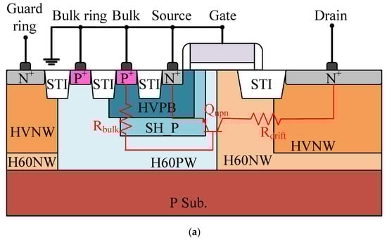

Figure 1.
(a) Parasitic equivalent circuit & cross-sectional view, (b) 3-D structure view, and (c) layout diagram of the high-voltage n-channel laterally diffused metal-oxide–semiconductor transistor (HV nLDMOS) reference device.
2.2. HV nLDMOSs with Drain Electrode-Embedded Horizontal Schottky Elements (Contact Rows Modulation)
In this study, we removed the N+ area in the nLDMOS_ref drain electrode to form an equivalent series Schottky area structure. Figure 2a,b display the 3D structure view and layout view, respectively, of the nLDMOS with the drain electrode parasitic full Schottky diode modulation. The nLDMOS formed a Schottky diode and series parasitic BJT-NPN. Arranging Schottky diodes in series increases the on-resistance of the HV nLDMOS.

Figure 2.
(a) 3D structure view and (b) layout diagram of the HV nLDMOS with the drain electrode-embedded full Schottky device modulation.
Figure 3a–c are the 3D structure diagram, layout view, and equivalent circuit of drain-electrode-embedded horizontal Schottky element modulation of the nLDMOS of the nLDMOS. The parasitic Schottky area was modulated by varying the row of contact of the Schottky area. The modulation method involves varying the Schottky area by symmetrically adding the contact windows laying on the top and bottom rows above the chip surface. The Schottky diode region was gradually increased to 2, 4, 8, 16, 32 and 36 rows of contact windows, and the effect of the increase in rows on ESD capability was observed. The ratio of the heavily doped N+ areas to Schottky diode areas is displayed in Table 1. Equivalently, from Figure 3c, the Ron will be increased as an HV nLDMOS by adding series Schottky diodes in the drain side. Under this parasitic Schottky structure, the drain electrode is equivalent to a series Schottky element and a high impedance R’drain. Furthermore, it is hoped that, through this technique, the It2 can be increased to improve the ESD withstanding capability of the device.
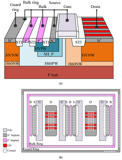

Figure 3.
(a) 3D structure view, (b) layout diagram, and (c) equivalent circuit of the HV nLDMOS with the drain electrode-embedded horizontal Schottky elements modulation.

Table 1.
Area ratios of N+ and Schottky diode regions in the drain side.
2.3. HV nLDMOSs with the Drain Electrode-Embedded Horizontal Schottky Elements (Length Modulation)
Next, another Schottky modulation for the upper and lower rows of contact windows were used as the variable parameter for Schottky length modulation. The Schottky area was then gradually reduced, which effectively reduced the length of the Schottky area by 1.5 μm on the left and right sides, 3 μm on the left and right sides, and 4.5 μm on the left and right sides. The effect of decreasing the ratio of the Schottky diode area and the length of the current path to the drain electrode on ESD capability was observed. Finally, the area ratio of heavily doped N+ to Schottky diode is listed in Table 2. Figure 4a,b display the structure and layout diagrams of HV nLDMOSs with the drain electrode-embedded horizontal Schottky length modulation.
Table 2.
Area ratios of N+ and Schottky diode regions in the drain electrode.

Figure 4.
(a) 3D structure view and (b) layout diagram of the HV nLDMOS with the drain electrode-embedded horizontal Schottky length modulation.
3. Test Method and Test Instrument
Transmission line pulse (TLP) systems [40,41,42] are generally used to measure the high-voltage and high-current snapback behavior of a test device. This TLP system uses LabVIEW software to control and match the peripheral electronic instruments such as ESD pulse generators, high-frequency digital oscilloscopes, and digital power meters, thus enabling automated measurement mechanisms. This machine can provide a continuous rising square wave to track the I–V characteristic curve of the DUTs, and the short rise and fall time of this continuous square wave can be used to simulate a fast ESD surge. The TLP system is used to simulate the human body model. Thus, the voltage and current response of the element can be obtained through element measurement, and the behavior of short ESD pulses on the protection device can be simulated. Through the TLP system, we can measure I–V characteristics, such as the trigger voltage (Vt1), holding voltage (Vh), secondary breakdown current (It2), and other physical parameters of the component.
4. Experimental Test Results
4.1. HV nLDMOSs with Drain Electrode-Embedded Horizontal Schottky Elements (Contact Rows Modulation)
The TLP tester system was used to measure the HV nLDMOS reference device and the DUTs characteristics with drain-electrode-embedded horizontal Schottky modulation (contact rows modulation). The snapback I–V characteristic curve, Vt1/Vh distribution, and secondary breakdown current distribution are displayed in Figure 5, Figure 6 and Figure 7, respectively. The number of contact window rows increased with the drain-electrode-embedded horizontal Schottky area to completely remove the heavily doped N+ area. Obviously, from Figure 3c, Schottky_Drain exhibited a higher secondary breakdown current performance than other DUTs because the drain electrode in the series Schottky diode increased the on-resistance (Ron) of the nLDMOS parasitic BJT. Meanwhile, through the measuring test, it can be found that an nLDMOS with the parasitic horizontal Schottky diode at the drain electrode had a limited effect on the breakdown voltage of the device. This modulation of the drain-electrode-embedded horizontal Schottky did not obviously influence the DC breakdown voltage (the maximum value only by 3.95%). Finally, all the measured parameters are displayed in Table 3. The Schottky area increased with the increase in the drain side, which increased It2 from 2.23 A in the nLDMOS reference device to a maximum of 4.55 A (104% improvement). From the measured data, it is found that the area of the parasitic Schottky diode in the drain side greatly affects the ESD capability. When the area percentage of an nLDMOS drain side added the Schottky diode exceeds 50%, the ESD robustness (It2) of the device is significantly increased. Then, the ESD immunity of nLDMOS was effectively improved by using these techniques.

Figure 5.
Snapback I-V curves and leakage currents of HV nLDMOSs with the drain electrode-embedded horizontal Schottky rows modulation.

Figure 6.
Trigger voltage and holding voltage distribution charts of HV nLDMOSs with the drain electrode-embedded horizontal Schottky rows modulation.

Figure 7.
Secondary breakdown-current distribution chart of HV nLDMOSs with the drain electrode-embedded horizontal Schottky rows modulation.
Table 3.
Snapback extracted parameters of HV nLDMOSs with the drain electrode-embedded horizontal Schottky rows modulation.
4.2. HV nLDMOSs with the Drain Electrode-Embedded Horizontal Schottky Elements (Length Modulations)
Furthermore, the Schottky length of the nLDMOS drain electrode was reduced to achieve modulation. The components were measured using the TLP tester. The snapback I–V characteristic curve, Vt1/Vh distribution, and secondary breakdown current distribution are displayed in Figure 8, Figure 9 and Figure 10, respectively. When the length of the Schottky area was decreased by reducing the length of the drain-electrode-embedded horizontal Schottky diode. The Schottky area of the drain electrode of the element gradually decreased, and the contact resistance of the drain electrode equivalent series to the Schottky diode also decreased. Similarly, through the measuring test, it can be found that an nLDMOS with the parasitic horizontal Schottky diode at the drain electrode of this modulation did not influence the DC breakdown voltage (the maximum value was only 2.51%). The secondary breakdown current of ESD immunity was reduced considerably. The measured parameters measured are displayed in Table 4. As the area of Schottky decreased to its minimum value, its It2 also reached the minimum (2.13 A).

Figure 8.
Snapback I-V curves and leakage currents of HV nLDMOSs with the drain electrode-embedded horizontal Schottky length modulation.

Figure 9.
Trigger voltage and holding voltage distribution charts of HV nLDMOSs with the drain electrode-embedded horizontal Schottky length modulation.

Figure 10.
Secondary breakdown-current distribution chart of HV nLDMOSs with the drain electrode-embedded horizontal Schottky length modulation.
Table 4.
Snapback extracted parameters of HV nLDMOSs with the drain electrode-embedded horizontal Schottky length modulation.
4.3. Summary of HV nLDMOSs with Drain Electrode-Embedded Horizontal Schottky Elements
As described above, the ESD capability (It2) value and Schottky-area percentage comparisons of HV nLDMOSs with the drain electrode-embedded horizontal Schottky elements by the row and length modulations are organized as shown in Figure 11a,b, respectively. According to the equivalent circuit diagram of Figure 3c, if the Schottky diode is parasitically embedded in the drain side of an nLDMOS, the ESD transient current under the action of an ESD will flow through the path (1) (the partial nLDMOS) and the path (2) (the parasitic Schottky diode). In the case of an HV nLDMOS with the drain electrode-embedded horizontal Schottky elements, the conduction-on resistance of this nLDMOS with a parasitic Schottky diode (path (2)) is higher than that of others nLDMOS part (path (1)). The main ESD current flows through the nLDMOS path (1). However, when the area of the Schottky diode increases, it means that the area of the drain-electrode for removing heavily doped N+ increases. Due to the low-doped NWell under the drain-electrode, it has a high impedance and favor to limit the ESD current. Therefore, when the Schottky area of the component is higher, the improvement of It2 is more obvious, especially as the area percentage of an nLDMOS drain side added to the Schottky diode exceeds 50%. When the area percentage of drain-side added the Schottky diode exceeds 94%, this ESD transient current cannot have more path options (it will be more uniform), the robustness (It2) of the device is significantly increased. This is also the reason why the It2 will be the highest value for an nLDMOS device with drain side covered 100% full parasitic Schottky diode. However, as the area ratio of the parasitic Schottky diode is small, the conduction path of the device is dominated by the nLDMOS path (1). Then, the characteristics of the parasitic series Schottky diode are not obvious. This leads to the lower It2 values of these components corresponding to Figure 11b.

Figure 11.
ESD capability (It2) values and Schottky-area % comparison of HV nLDMOSs with the drain electrode-embedded horizontal Schottky elements by the (a) row modulation and (b) length modulation.
5. Conclusions
This study described the effect of the drain-electrode of horizontal Schottky modulation on ESD protection. When the contact row modulation was performed for the drain-electrode-embedded horizontal Schottky diode, the area of the Schottky diode gradually increased. Under the parasitic Schottky structure of part or all of the drain electrode, the equivalent ON-resistance of the overall HV LDMOS device will be increased. Therefore, a higher Schottky area in the drain electrode of the element results in a higher secondary breakdown current. The component can withstand a larger ESD current. Therefore, when the area of the drain electrode Schottky diode increases, the ESD immunity will increase significantly, especially when the area percentage of the Schottky diode exceeds 50%. Especially, when the nLDMOS drain side is all covered with the parasitic Schottky diode, its ESD capability (It2) will increase from 2.23 A in the nLDMOS Reference device to a maximum value of 4.55 A (an increase of 104%). The It2 was excellent, and the ESD protection capability of the device was also satisfactory.
Author Contributions
Conceptualization, S.-Z.H. and S.-L.C.; data curation, S.-Z.H.; formal analysis, S.-Z.H.; investigation, S.-Z.H. and S.-L.C.; project administration, S.-L.C.; supervision, S.-L.C.; validation, S.-Z.H. and S.-L.C.; writing—original draft, S.-Z.H.; writing—review and editing, S.-L.C. All authors have read and agreed to the published version of the manuscript.
Funding
This research was no external funding.
Data Availability Statement
Data can be provided according to industry R&D requirements (The data used in the study may be available depending on the corresponding author).
Acknowledgments
In this work, the authors would like to thank the Taiwan Semiconductor Research Institute in Taiwan for providing the process information and fabrication platform of TSMC.
Conflicts of Interest
The authors declare no conflict of interest.
Nomenclature
| BCD | Bipolar-CMOS-DMOS |
| BJT | Bipolar transistor |
| ESD | Electrostatic discharge |
| GDT | Gas discharge tube |
| HV | High-voltage |
| It2 | Secondary breakdown current |
| LDMOS | Lateral diffused metal-oxide-semiconductor transistor |
| SPG | Spark gap |
| STI | Shallow trench isolation |
| TLP | Transmission-line Pulse |
| TVS | Transient voltage suppressor |
| VDR | Voltage-dependent resistor |
| Vh | Holding voltage |
| VLSI | Very-large-scale integration |
| Vt1 | Trigger voltage |
References
- Xi, Y.; Malobabic, S.; Vashchenko, V.; Liou, J. Correlation between TLP, HMM, and System-Level ESD Pulses for Cu Metallization. IEEE Trans. Device Mater. Reliab. 2014, 14, 446–450. [Google Scholar] [CrossRef]
- Lee, J.H.; Iyer, N.M. Analytical Model of Correlation Factor for Human-Body Model to Transmission-Line Pulse ESD Testing. IEEE Electron Device Lett. 2017, 38, 952–954. [Google Scholar] [CrossRef]
- Lai, D.W.; Raad, G.D.; Tseng, W.J.; Smedes, T.; Huitsing, A.J. Bidirectional ESD Protection Device Using PNP with pMOS-Controlled Nwell Bias. IEEE Electron Device Lett. 2018, 39, 331–334. [Google Scholar] [CrossRef]
- Lai, D.W.; Raad, G.D.; Sque, S.; Peters, W.; Smedes, T. High-Voltage ESD Protection Device With Fast Transient Reaction and High Holding Voltage. IEEE Trans. Electron Devices 2019, 66, 2884–2891. [Google Scholar] [CrossRef]
- Coyne, E.; Clarke, D.; Heffernan, S.; Moane, B. Designing ESD Protection Devices for Ultrafast Overvoltage Events. IEEE Trans. Electron Devices 2019, 66, 4850–4857. [Google Scholar] [CrossRef]
- Chang, R.; Ker, M. Design of High-Voltage-Tolerant Power-Rail ESD Protection Circuit for Power Pin of Negative Voltage in Low-Voltage CMOS Processes. IEEE Trans. Electron Devices 2020, 67, 40–46. [Google Scholar] [CrossRef]
- Viale, B.; Allard, B. Scalable and Versatile Design Guidance Tool for the ESD Robustness of Integrated Circuits—Part I. IEEE Trans. Comput. Aided Des. Integr. Circuits Syst. 2020, 39, 3067–3080. [Google Scholar] [CrossRef]
- Viale, B.; Allard, B. Scalable and Versatile Design Guidance Tool for the ESD Robustness of Integrated Circuits—Part II. IEEE Trans. Comput. Aided Des. Integr. Circuits Syst. 2020, 39, 3107–3117. [Google Scholar] [CrossRef]
- Chen, S.; Wu, P.; Chen, Y. Robust ESD-Reliability Design of 300-V Power N-Channel LDMOSs with the Elliptical Cylinder Super-Junctions in the Drain Side. Electronics 2020, 9, 730. [Google Scholar] [CrossRef]
- Fan, S.; Chen, S.; Lin, P.; Chen, H. Layout Strengthening the ESD Performance for High-Voltage N-Channel Lateral Diffused MOSFETs. Electronics 2020, 9, 718. [Google Scholar] [CrossRef]
- Radić, A.; Lukić, Z.; Prodić, A.; de Nie, R.H. Minimum-Deviation Digital Controller IC for DC–DC Switch-Mode Power Supplies. IEEE Trans. Power Electron. 2013, 28, 4281–4298. [Google Scholar] [CrossRef]
- Siwakoti, Y.P.; Blaabjerg, F.; Loh, P.C. Quasi-Y-Source Boost DC–DC Converter. IEEE Trans. Power Electron. 2015, 30, 6514–6519. [Google Scholar] [CrossRef]
- Kennedy, S.; Yuce, M.R.; Redouté, J.M. Fully Integrated Switched-Capacitor DC/DC Converters with Clock Slope EMI Control. IEEE Trans. Electromagn. Compat. 2018, 60, 2073–2075. [Google Scholar] [CrossRef]
- Sun, Y.; Kang, X.; Zheng, Y.; Lu, J.; Tian, X.; Wei, K.; Wu, H.; Wang, W.; Liu, X.; Zhang, G. Review of the Recent Progress on GaN-Based Vertical Power Schottky Barrier Diodes (SBDs). Electronics 2019, 8, 575. [Google Scholar] [CrossRef]
- Guo, X.; Xun, Q.; Li, Z.; Du, S. Silicon Carbide Converters and MEMS Devices for High-temperature Power Electronics: A Critical Review. Micromachines 2019, 10, 406. [Google Scholar] [CrossRef]
- Guo, Z.; Li, H.; Liu, C.; Zhao, Y.; Su, W. Stability-improvement method of cascaded DC-DC converters with additional voltage-error mutual feedback control. Chin. J. Electr. Eng. 2019, 5, 63–71. [Google Scholar] [CrossRef]
- Liu, X.; Tan, C. First-principle investigation of monoclinic (AlxInyGa1-x-y)2O3 quaternary alloy. Semicond. Sci. Technol. 2020, 35, 025023. [Google Scholar] [CrossRef]
- Wu, C.; Guo, D.Y.; Zhang, L.Y.; Li, P.G.; Zhang, F.B.; Tan, C.K.; Wang, S.L.; Liu, A.P.; Wu, F.M.; Tang, W.H. Systematic investigation of the growth kinetics of β-Ga2O3 epilayer by plasma enhanced chemical vapor deposition. Appl. Phys. Lett. 2020, 116, 072102. [Google Scholar] [CrossRef]
- Liang, S.; Wang, J.; Deng, L.; Fang, F.; John Shen, Z. Monolithic Integration of SiC Power BJT and Small-Signal BJTs for Power ICs. IEEE J. Emerg. Sel. Top. Power Electron. 2020, 8, 24–30. [Google Scholar] [CrossRef]
- De Alcântara Bastos, G.H.; Costa, L.F.; Tofoli, F.L.; Torrico Bascopé, G.V.; Torrico Bascopé, R.P. Nonisolated DC–DC Converters with Wide Conversion Range for High-Power Applications. IEEE J. Emerg. Sel. Top. Power Electron. 2020, 8, 749–760. [Google Scholar] [CrossRef]
- Chang, J.; Moon, S.; Lee, G.; Hwang, P. A New Local Control Method of Interlinking Converters to Improve Global Power Sharing in an Islanded Hybrid AC/DC Microgrid. IEEE Trans. Energy Convers. 2020, 35, 1014–1025. [Google Scholar] [CrossRef]
- Liu, X.; Sammarco, C.; Zeng, G.; Guo, D.; Tang, W.; Tan, C. Investigations of monoclinic- and orthorhombic-based (BxGa1-x)2O3 alloys. Appl. Phys. Lett. 2020, 117, 012104. [Google Scholar] [CrossRef]
- Wu, J.; Lu, Y. Decoupling and Optimal Control of Multilevel Buck DC–DC Converters with Inverse System Theory. IEEE Trans. Ind. Electron. 2020, 67, 7861–7870. [Google Scholar] [CrossRef]
- Sangrody, R.; Pouresmaeil, M.; Marzband, M.; Pouresmaeil, E. Resonance-Based Optimized Buck LED Driver Using Unequal Turn Ratio Coupled Inductance. IEEE Trans. Power Electron. 2020, 35, 13068–13076. [Google Scholar] [CrossRef]
- Nela, L.; Van Erp, R.; Kampitsis, G.; Yildirim, H.K.; Ma, J.; Matioli, E. Ultra-compact, High-Frequency Power Integrated Circuits Based on GaN-on-Si Schottky Barrier Diodes. IEEE Trans. Power Electron. 2021, 36, 1269–1273. [Google Scholar] [CrossRef]
- Tsai, H.; Ker, M. Latch-Up Protection Design with Corresponding Complementary Current to Suppress the Effect of External Current Triggers. IEEE Trans. Device Mater. Reliab. 2015, 15, 242–249. [Google Scholar] [CrossRef]
- Zhang, C.; Liu, S.; Xu, K.; Wei, J.; Ye, R.; Sun, W.; Su, W.; Zhang, A.; Ma, S.; Lin, F.; et al. A Novel High Latch-Up Immunity Electrostatic Discharge Protection Device for Power Rail in High-Voltage ICs. IEEE Trans. Device Mater. Reliab. 2016, 16, 266–268. [Google Scholar] [CrossRef]
- Duan, B.; Licheng, S.; Yang, Y. Analysis of the Novel Snapback-Free LIGBT with Fast-Switching and Improved Latch-Up Immunity by TCAD Simulation. IEEE Electron Device Lett. 2019, 40, 63–66. [Google Scholar] [CrossRef]
- Chen, C.; Ker, M. Optimization Design on Active Guard Ring to Improve Latch-Up Immunity of CMOS Integrated Circuits. IEEE Trans. Electron Devices 2019, 66, 1648–1655. [Google Scholar] [CrossRef]
- Paul, M.; Kumar, B.S.; Gossner, H.; Shrivastava, M. Engineering Schemes for Bulk FinFET to Simultaneously Improve ESD/Latch-Up Behavior and Hot Carrier Reliability. IEEE Trans. Electron Devices 2020, 67, 2745–2751. [Google Scholar] [CrossRef]
- He, L.; Salcedo, J.A.; Parthasarathy, S.; Hajjar, J.; Sundaram, K. A New Low-Capacitance High-Voltage-Tolerant Protection Clamp for High-Speed Applications. IEEE Trans. Electron Devices 2020, 67, 3030–3034. [Google Scholar] [CrossRef]
- Coyne, E.; Geary, S.; Brannick, A.; Meskel, J. Parasitic NPN and PNP Latch-Up within a Single DMOS for High Voltage Reliability. IEEE Trans. Electron Devices 2020, 67, 3291–3297. [Google Scholar] [CrossRef]
- Li, W.; Nomoto, K.; Pilla, M.; Pan, M.; Gao, X.; Jena, D.; Xing, H.G. Design and Realization of GaN Trench Junction-Barrier-Schottky-Diodes. IEEE Trans. Electron Devices 2017, 64, 1635–1641. [Google Scholar] [CrossRef]
- Wei, J.; Zhang, M.; Jiang, H.; Zhou, X.; Li, B.; Chen, K.J. Superjunction MOSFET with Dual Built-In Schottky Diodes for Fast Reverse Recovery: A Numerical Simulation Study. IEEE Electron Device Lett. 2019, 40, 1155–1158. [Google Scholar] [CrossRef]
- Kun, C.; He, Y.; Li, Y.; Ng, A.; Yu, J. A Room Temperature Hydrocarbon Electronic Nose Gas Sensor Based on Schottky and Heterojunction Diode Structures. IEEE Electron Device Lett. 2020, 41, 163–166. [Google Scholar] [CrossRef]
- Mao, L.F. Hot-Carriers’ Effect on the Performance of Organic Schottky Diodes. IEEE Access 2020, 8, 65970–65982. [Google Scholar] [CrossRef]
- Li, P.; Guo, J.; Lin, Z.; Hu, S.; Shi, C.; Tang, F. A Low-Reverse-Recovery-Charge Superjunction MOSFET with P-Base and N-Pillar Schottky Contacts. IEEE Trans. Electron Devices 2020, 67, 1693–1698. [Google Scholar] [CrossRef]
- Yi, B.; Lin, J.; Zhang, B.; Cheng, J.; Xiang, Y. Simulation Study of a Novel Snapback Free Reverse-Conducting SOI-LIGBT with Embedded P-Type Schottky Barrier Diode. IEEE Trans. Electron Devices 2020, 67, 2058–2065. [Google Scholar] [CrossRef]
- Reinke, P.; Benkhelifa, F.; Kirste, L.; Czap, H.; Pinti, L.; Zürbig, V.; Cimalla, V.; Nebel, C.; Ambacher, O. Influence of Different Surface Morphologies on the Performance of High-Voltage, Low-Resistance Diamond Schottky Diodes. IEEE Trans. Electron Devices 2020, 67, 2471–2477. [Google Scholar] [CrossRef]
- Wang, Y.; Wang, Y.; Lu, G.; Du, G.; Zhang, X.; Huang, R. Modeling IC components based on TLP I-V curves and transient responses from SEED perspective. In Proceedings of the 2018 IEEE International Symposium on Electromagnetic Compatibility and 2018 IEEE Asia-Pacific Symposium on Electromagnetic Compatibility (EMC/APEMC), Singapore, 14–18 May 2018; pp. 862–865. [Google Scholar] [CrossRef]
- Gardella, P.J.; Baez, E.; Cesaretti, J.M. Design of ESD protections for ECG applications. In Proceedings of the 2020 Argentine Conference on Electronics (CAE), Buenos Aires, Argentina, 27–28 February 2020; pp. 104–107. [Google Scholar] [CrossRef]
- Wang, Y.; Wang, Y. A New Method to Correlate Human Body Model and Transmission Line Pulse Based on RC Thermal Equivalent Model. IEEE Trans. Electron Devices 2020, 67, 3775–3780. [Google Scholar] [CrossRef]
Publisher’s Note: MDPI stays neutral with regard to jurisdictional claims in published maps and institutional affiliations. |
© 2021 by the authors. Licensee MDPI, Basel, Switzerland. This article is an open access article distributed under the terms and conditions of the Creative Commons Attribution (CC BY) license (http://creativecommons.org/licenses/by/4.0/).