Article

A Fast Lock All-Digital MDLL Using a Cyclic Vernier TDC for Burst-Mode Links

1
Samsung Electronics, System LSI, Gyeonggi 446711, Korea
2
Department of Electronic and Electrical Engineering, Hongik University, Seoul 06983, Korea
*
Author to whom correspondence should be addressed.
Electronics 2021, 10(2), 177; https://doi.org/10.3390/electronics10020177
Submission received: 14 December 2020 / Revised: 11 January 2021 / Accepted: 13 January 2021 / Published: 15 January 2021
(This article belongs to the Special Issue Mixed-Signal VLSI Design)

Abstract

:
An all-digital multiplying delay-locked loop (MDLL)-based clock multiplier featuring a time-to-digital converter (TDC) to achieve fast power-on capability is presented. The proposed MDLL adopts a new offset-free cyclic Vernier TDC to achieve a fast lock time of 15 reference clock cycles while maintaining a wide detection range and high resolution. The proposed offset-free TDC also uses a correlated double sampling technique to remove mismatch and offset issues, resulting in low jitter characteristics. After the MDLL is quickly locked, the TDC is turned off, and it goes into delta-sigma modulator (DSM)-based sequential tracking mode to reduce power consumption and improve jitter performance. Implemented in a 65-nm 1.0-V CMOS process, the proposed MDLL occupies an active area of 0.043 mm2 and generates a 2.4-GHz output clock from a 75-MHz reference clock (multiplication factor N = 32). It achieves an effective peak-to-peak jitter of 9.4 ps and consumes 3.3 mW at 2.4 GHz.

1. Introduction

As the demand for high-speed off-chip I/O bandwidth in computing systems increases, the importance of energy efficiency of serial links is rapidly increasing. One approach to address this problem is to use burst-mode communication. Burst-mode data communication, traditionally applied to passive optical networks (PONs), has recently begun to be applied to electrical chip-to-chip serial links [1,2,3,4]. In conventional serial links, there is idle power consumed by transceivers even when the link is not in use. However, in a burst-mode-based energy proportional link [4], energy efficiency can be increased because the link and transceivers are powered-on/-off rapidly only when there is a data transmission request.
One of the most critical building blocks in this high-speed energy proportion link design is a fast power-on (or fast lock) clock multiplier for burst-mode operation. The fast power-on/-off clock multiplier should have the ability to quickly multiply the reference clock and complete the phase lock to generate a de-skewed high-frequency output clock.
In general, clock multipliers have been designed based on phase-locked loops (PLLs). However, the loop bandwidth of a typical PLL cannot be easily increased to shorten the lock time due to stability problems [5]. Various techniques have been proposed in the PLL structure to reduce the locking time. Among the PLLs showing reasonable power and performance, the digital PLL from [6] achieved a lock time of forty reference clock cycles, which is insufficient for use in burst mode serial link applications.
In this paper, instead of using a PLL, we introduce a clock multiplier technology that uses a digital multiplying delay-locked loop (MDLL) to obtain fast lock characteristics. A typical MDLL generates the output clock frequency fclkout that is N times the reference clock frequency fclkref, where N is the frequency multiplication factor [7,8,9,10,11,12,13,14,15,16,17,18,19]. Figure 1 shows the block diagram of a typical MDLL. It consists of a multiplexer (MUX), a multiplexed ring oscillator (MRO), a phase detector (PD), a charge pump (CP) + loop filter (LF), a divider N, and a select logic. By periodically injecting a clean reference clock edge, the MDLL can achieve better jitter performance with reduced loop bandwidth limit issues. The extended loop bandwidth of the MDLL can bring fast lock characteristics, but most of the MDLLs presented so far have been mainly concerned with jitter and phase noise characteristics.
Among the various all-digital MDLL architectures [8,9,10,11,12,13,14,15,16,17,18,19], the work from digital MDLL [14] achieved a lock time of forty clock cycles by using a successive approximation register (SAR)-based binary search algorithm. To further improve the locking time of a digital MDLL, we propose a new method of using a time-to-digital converter (TDC) [20,21,22,23,24,25,26] in this paper. Conventionally, the purpose of using a TDC in digital MDLL design was to generate a digital bit proportional to the phase difference between two inputs by replacing a phase detector (PD). Since the quantization error of a TDC causes a jitter increase, the main issue of conventional TDC-based MDLLs was in the design of a high-resolution TDC with low power consumption [8,13]. In these conventional digital MDLLs, low jitter and low reference spur characteristics were the main concern, and little attention was paid to fast power-on or locking time.
In this paper, we present a new all-digital MDLL that features a cyclic Vernier TDC to achieve fast power-on capability. This is the first fast lock all-digital MDLL that utilizes a cyclic Vernier architecture [20,21,22,23,24,25,26] to achieve a wide detection range and high resolution. The rest of this paper is organized as follows. Section 2 presents the architecture and operation of the proposed all-digital MDLL, Section 3 shows the experimental results, and Section 4 presents the conclusion.

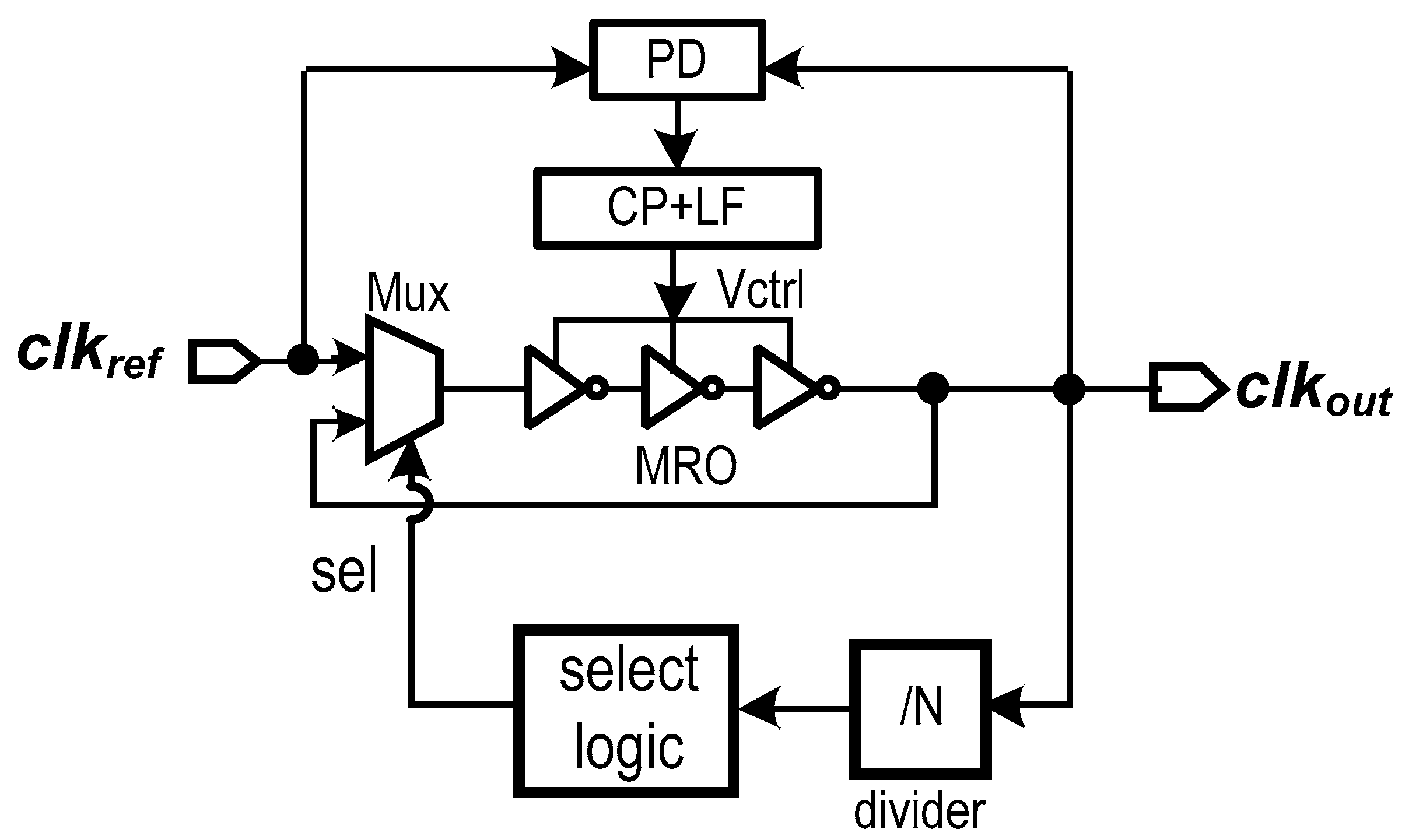
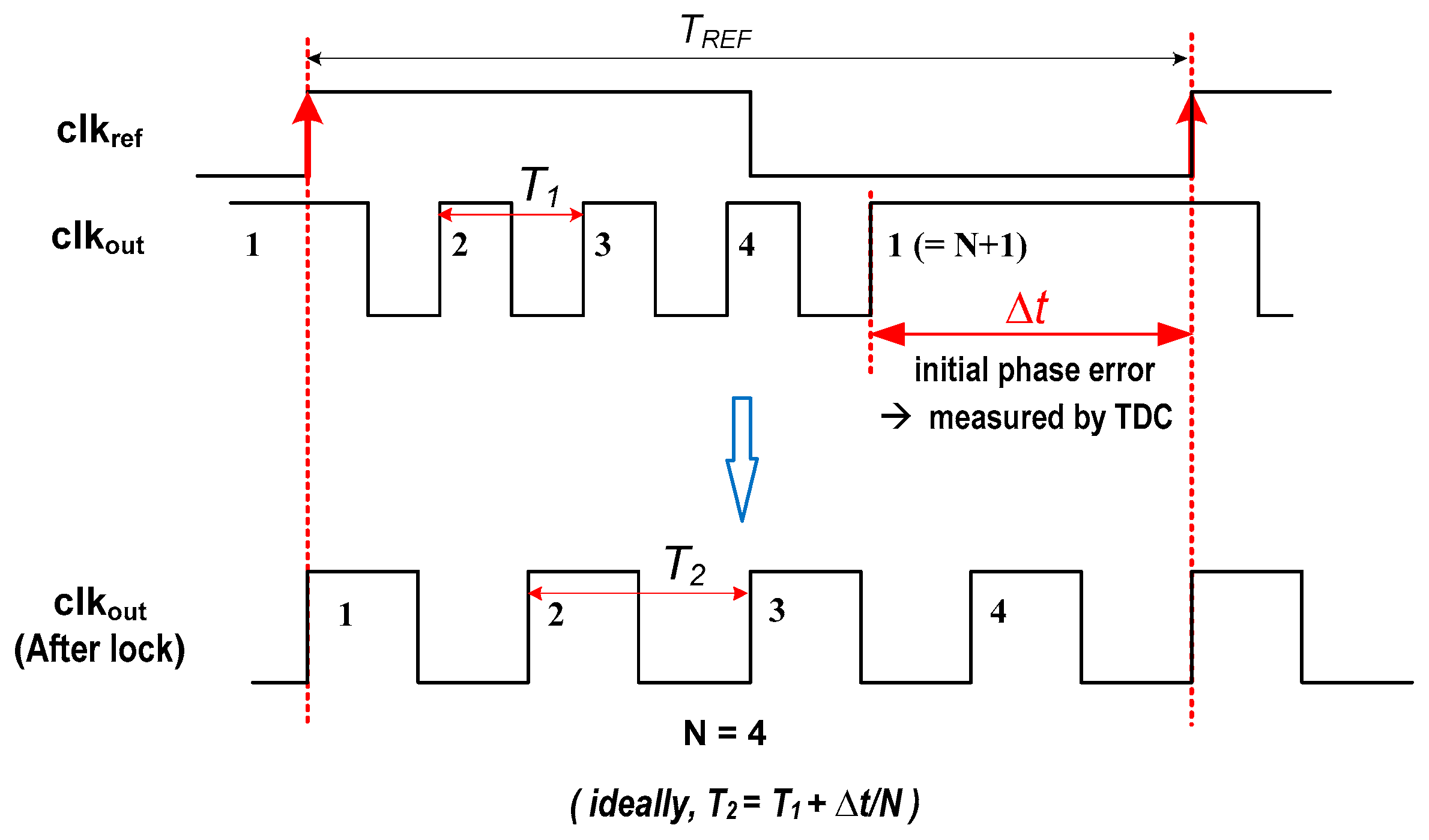
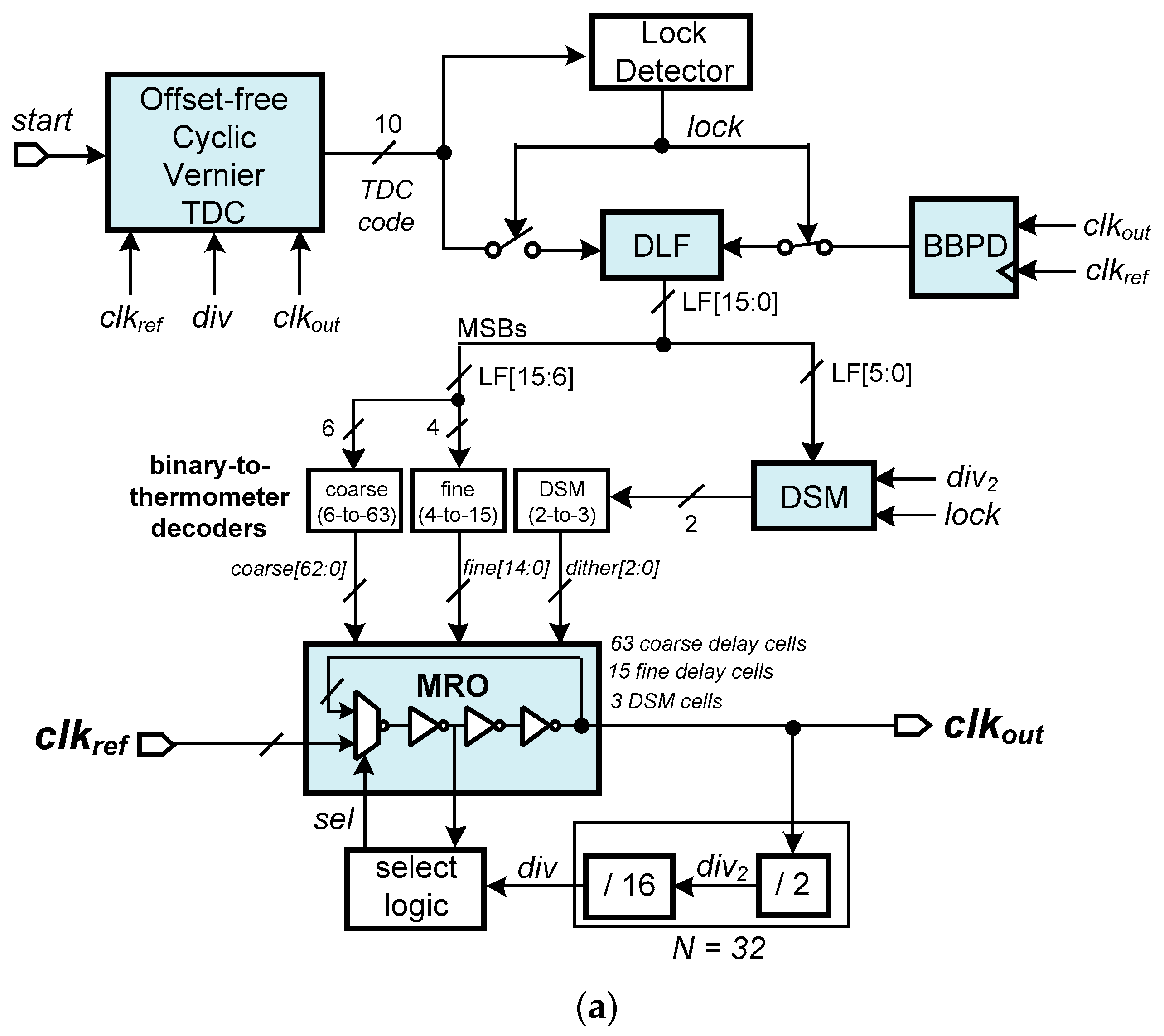
2. Proposed All-Digital MDLL

2.1. Proposed MDLL Architecture

Figure 2 shows a conceptual diagram of the proposed MDLL detecting the initial phase error (=∆t) using a TDC at the beginning of the operation, where TREF is the period of the reference clock (clkref), T1 is the period of the initial output clock (clkout), and T2 is the period of the clkout after locking. Ideally, T2 = T1 + ∆t/N after locking, where N is the frequency multiplication factor.
Figure 3a shows the proposed all-digital MDLL architecture, which consists of an offset-free cyclic Vernier TDC, a lock detector (LD), a digital loop filter (DLF), a bang-bang phase detector (BBPD), a second-order delta-sigma modulator (DSM), three binary-to-thermometer decoders (coarse/fine/DSM), a digitally controlled multiplexed ring oscillator (MRO), a/16 frequency divider, a/2 frequency divider, and a select logic. The MRO is a pseudo-differential inverter with three types of varactor delay cells (63 coarse delay cells, 15 fine delay cells, 3 DSM cells). As shown in Figure 3b, the proposed MDLL has two operation modes: TDC mode and sequential tracking mode. When the proposed MDLL is enabled, the MRO starts at the maximum operating frequency. The proposed cyclic Vernier TDC measures the initial phase error (Δt) between the N + 1th rising edge of clkout and the rising edge of clkref (as shown in Figure 2) and converts this Δt value to a 10-bit digital TDC code. Then, the TDC code is filtered by the DLF. And the DLF generates the 16-bit LF [15:0] signal. The three decoders generate signals (coarse [62:0], fine [14:0], and dither [2:0]) that control the delay of the MRO.
The coarse decoder utilizes the six most-significant-bits (MSBs) of the LF [15:0] to generate the thermometer code signal (coarse [62:0]) that adjusts the programmable delay value of the coarse delay cells of the MRO. Similarly, the fine decoder utilizes the LF [9:6] signal to provide the fine [14:0] signal that adjusts the fine delay cells of the MRO. The DLF’s 6-bit least-significant-bits (LSBs) are used for the DSM, and the DSM decoder generates the dither [2:0] signal that controls the DSM cells of the MRO at high speed. Here, the sum of the programmable delay of the 15 fine delay cells is equal to the delay of one coarse delay cell. The delay resolution of the DSM cell and that of the fine delay cell are the same.
As shown in Figure 3b, in the TDC mode, the TDC search can be repeatedly performed several times. Each TDC search requiring three reference clock cycles uses a correlated double sampling technique [13,27] to eliminate mismatch and offset issues. Ideally, the TDC mode can be completed with only one TDC search. However, the mismatch problem between the MRO and TDC remains unless offset calibration is used, which leads to repetitive TDC searches. A single TDC search takes three TREF cycles, and the TDC mode is completed through a maximum of five TDC search iterations. Subsequently, when phase lock is completed, the LD generates the lock signal, and the MDLL enters the sequential tracking mode. In this sequential tracking mode, the TDC is turned off, and both the BBPD and the DSM are enabled. Therefore, after fast phase locking, the MDLL operates in a closed-loop and can track the process, voltage, and temperature (PVT) and environment variations while simultaneously reducing power consumption and improving jitter performance. The DSM receives 6-bit LSBs, LF [5:0], of the DLF and generates a 2-bit binary signal with a frequency 16 times higher than the BBPD operating frequency. Then, the DSM decoder generates dither [2:0] signals operating at high speed to control the DSM cells of the MRO, which effectively reduces the dithering jitter of the digital MDLL [15].

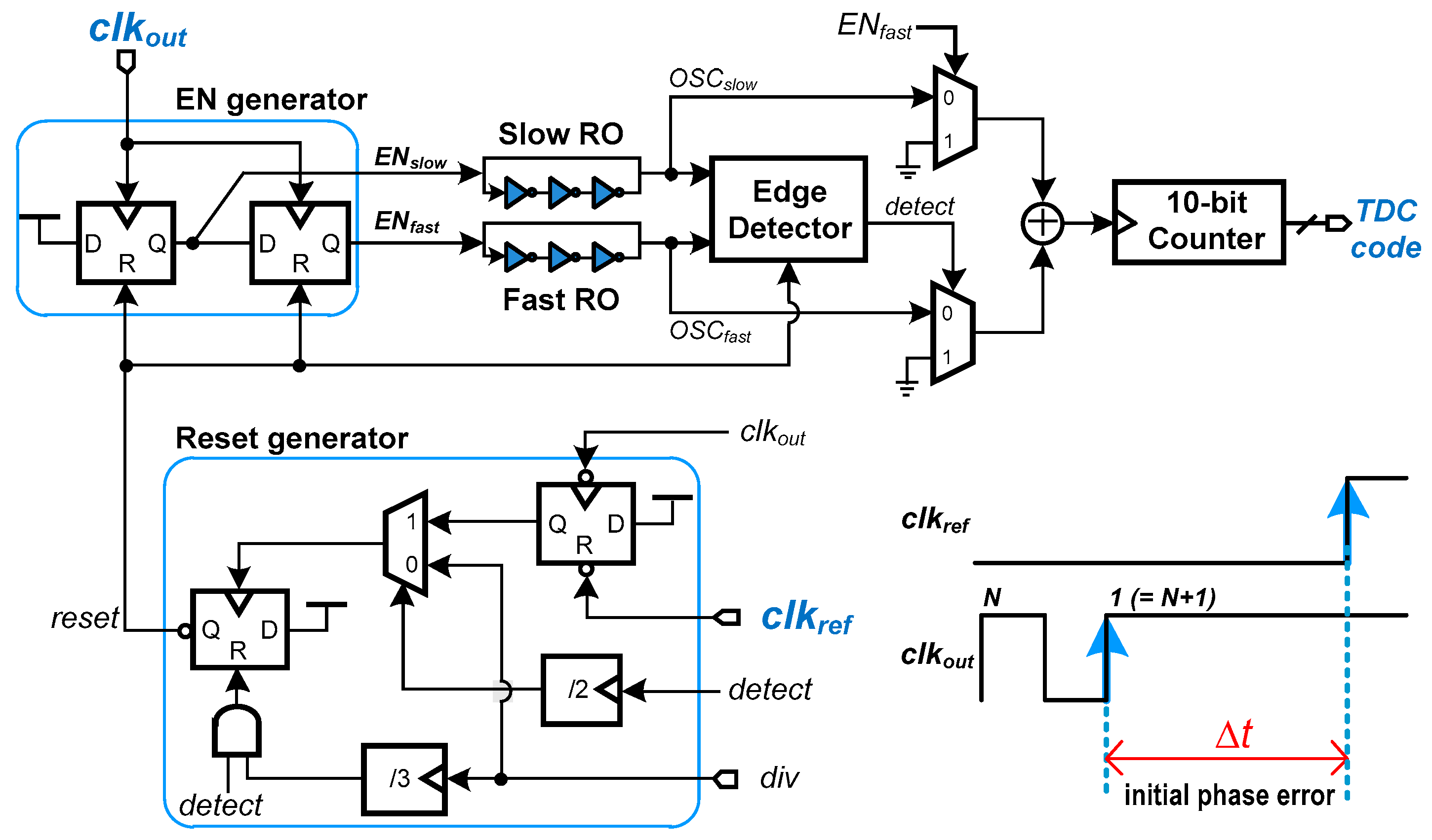
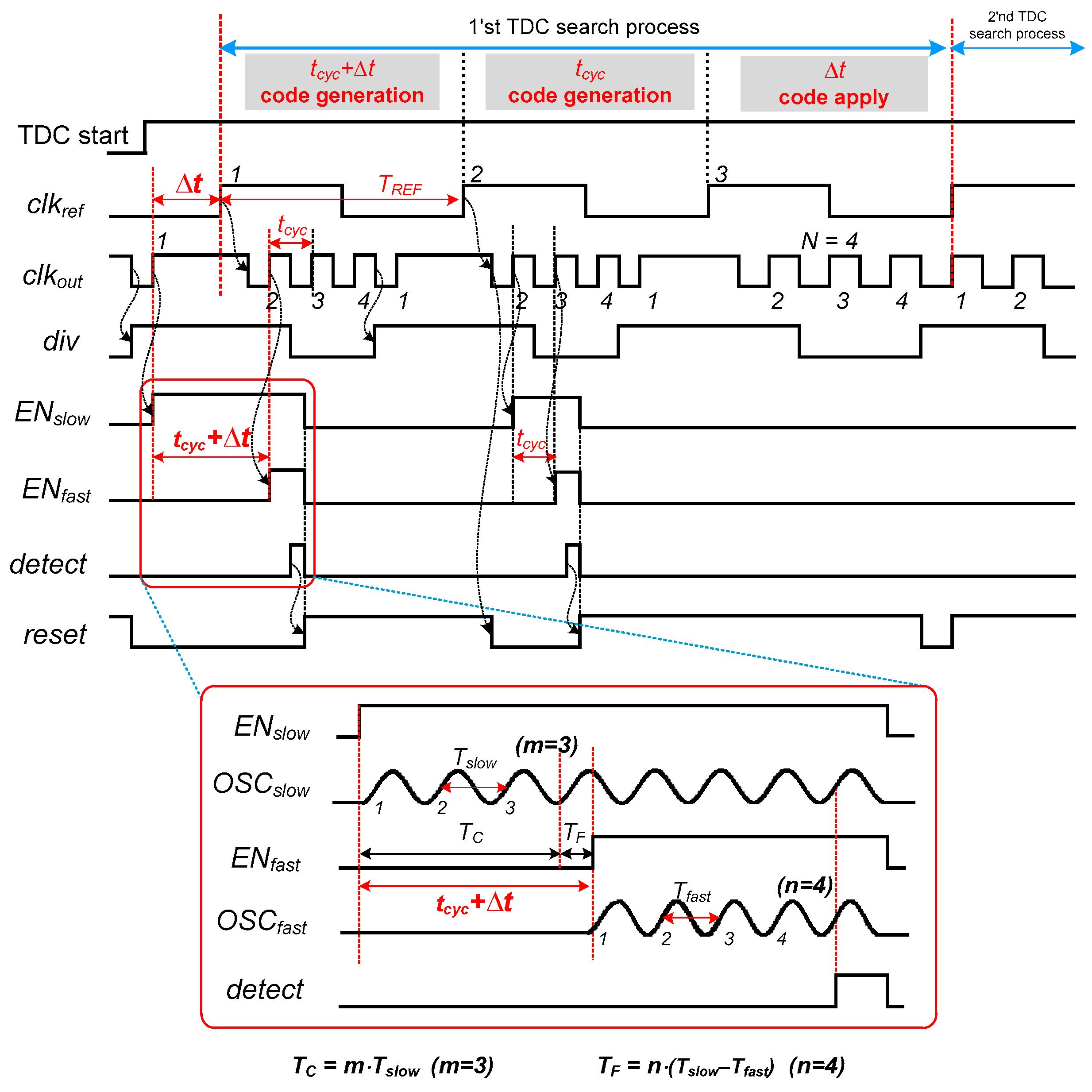
2.2. Proposed Offset-Free Cyclic Vernier TDC

Figure 4 shows the block diagram of the proposed offset-free cyclic Vernier TDC. The proposed TDC consists of an EN generator, a reset generator, a slow ring oscillator (RO), a fast RO, an edge detector, two multiplexers, and a 10-bit up/down counter. The fast RO has a period of Tfast that is slightly faster than Tslow. As shown in the lower right Figure 4, the TDC is used to measure the initial phase error (=∆t) between the N + 1 th rising edge of clkout and the rising edge of clkref.
Figure 5 shows the detailed operation process of the proposed TDC mode with an example of N = 4. Each TDC search process takes three reference clock cycles. When the TDC is activated, the EN generator creates the ENslow and ENfast signals that enable the two ROs. The initial phase difference between these two signals is equal to tcyc + ∆t, where tcyc is the free-running period of the clkout (=output of the MRO). The 10-bit counter counts the oscillation number (=m) of the OSCslow signal during the time from the rising edge of the ENslow to the rising edge of the ENfast. Instead of using two separate counters, the 10-bit counter counts the oscillation number (=n) of the OSCfast again during the time from the rising edge of the ENfast to the rising edge of the detect signal: in this example, m = 3 and n = 4. The edge detector shown in Figure 4 compares the OSCslow and OSCfast signals and generates the detect signal when the rising edge of OSCfast leads to the rising edge of OSCslow. The detect signal makes the reset signal go to logic high, making the outputs of the EN generator fall to logic low. Then, the detect signal falls to logic low again. As a result, in the first reference clock cycle, tcyc + ∆t is measured and can be determined as follows:
t c y c + Δ t = T C + T F = m · T s l o w + n · ( T s l o w T f a s t )
where TC is the coarse delay, TF is the fine delay, and Tslow − Tfast is the fine resolution of the proposed TDC. Similarly, the second reference clock cycle is used to measure the tcyc. By subtracting the code value of the second cycle from the code value of the first cycle, the required initial phase error ∆t can be obtained. The third reference clock cycle is used to apply this subtracted TDC code to the DLF and the MRO, and accordingly, the delay of the MRO is changed, and the MDLL approaches the coarse phase lock state.
When the TDC measures the time difference, there can always be a time offset, ∆offset. This ∆offset is caused by analog nonidealities, such as signal path mismatch and device mismatch, and causes a problem of increasing the deterministic jitter of an MDLL. To overcome this problem, the proposed TDC mode adopts a correlated double-sampling technique [13,22] to eliminate mismatch and offset problems and improve jitter performance.
In Figure 5, what the TDC actually measures in the first sampling period is not tcyc + ∆t but tcyc + ∆t + ∆offset, which is a value including the time offset ∆offset. The value measured in the second sampling period is not tcyc, but tcyc + ∆offset. Therefore, if the values of two consecutive measurement codes are subtracted from each other, the ∆offset can be removed, and the correct ∆t can be obtained. When the ∆t value becomes smaller than the resolution (=Tslow − Tfast = 6 ps in this design) of the Vernier TDC after up to a maximum of five TDC searches are performed, the lock detector generates the lock signal, and the MDLL enters the sequential tracking mode. Then, the TDC is disabled to reduce power consumption, and both the BBPD and the DSM are enabled.
The lower six-bits, LF [5:0], of the DLF output, are used for the DSM. The DSM operates 16 times faster than the reference clock and generates a 2-bit signal for the DSM decoder. Then, the DSM decoder generates dither [2:0], which controls the three DSM cells at high frequency. This DSM-based dithering jitter reduction scheme brings the advantage of greatly improving the deterministic jitter performance of the proposed MDLL with a large N value [15].

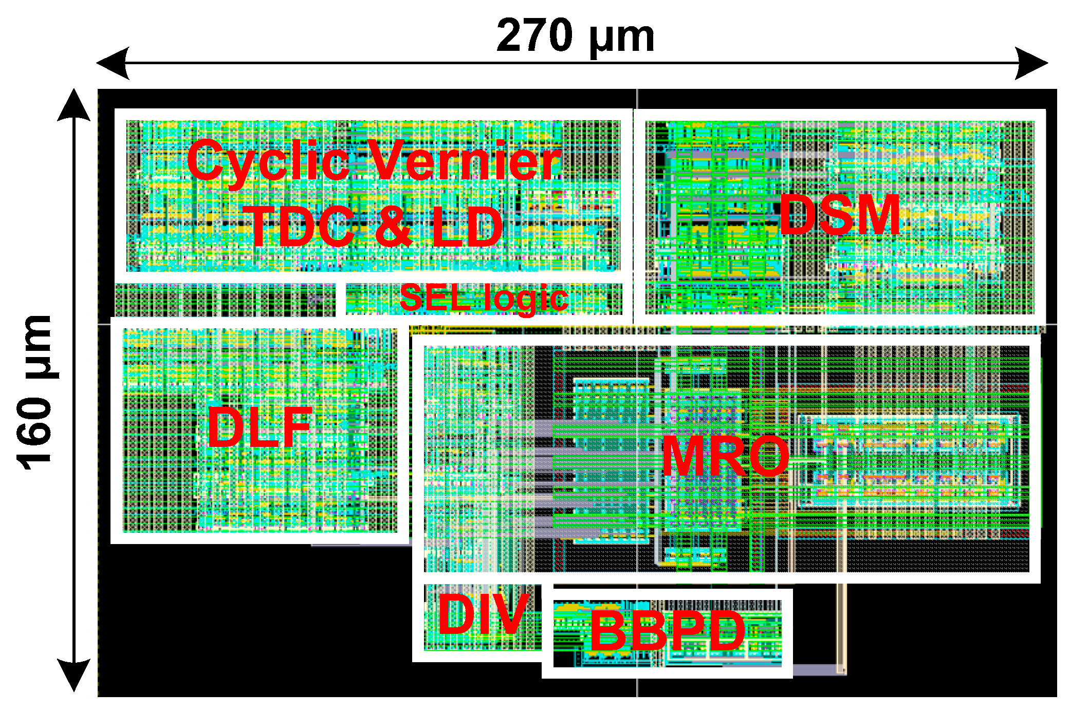
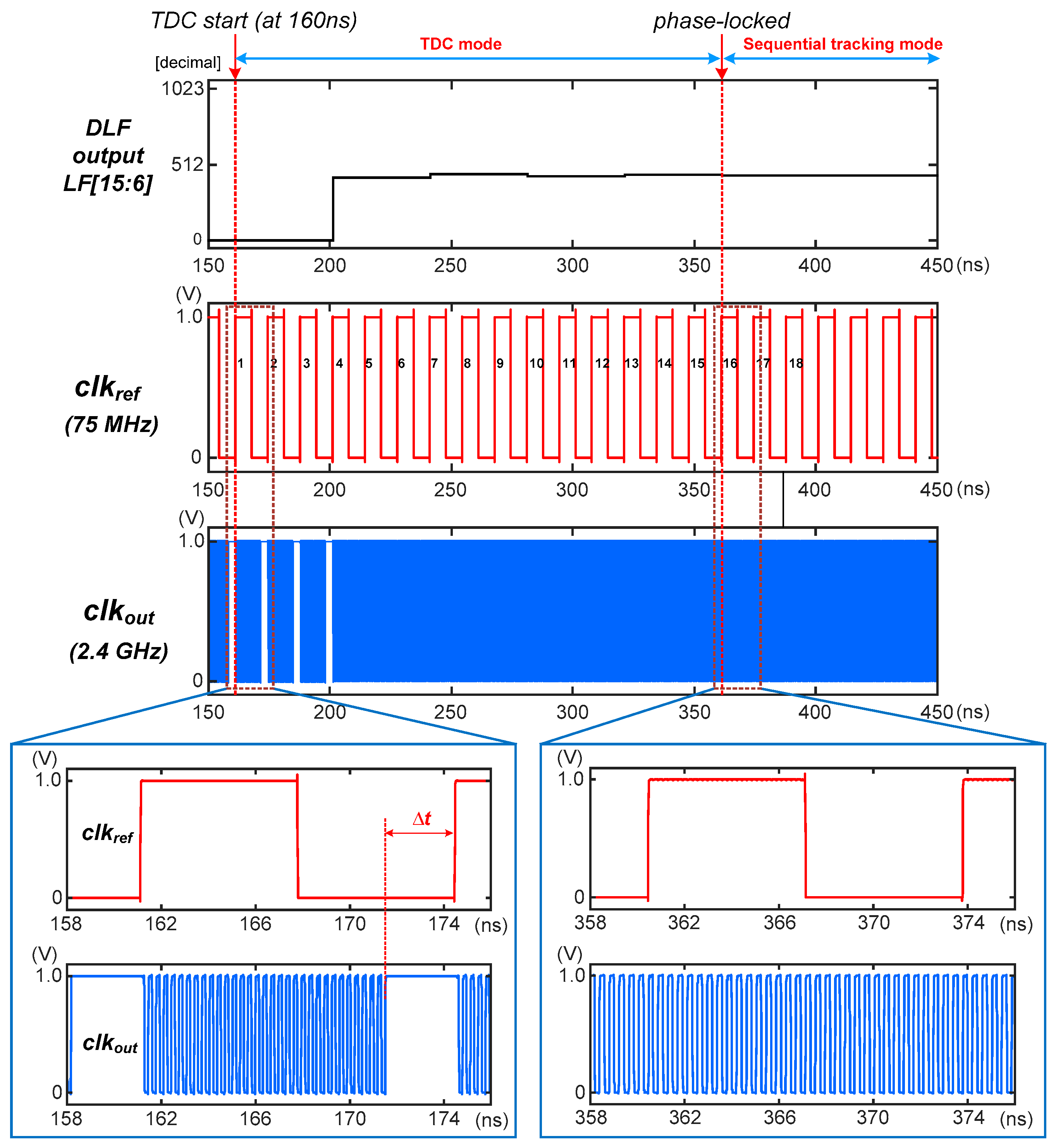
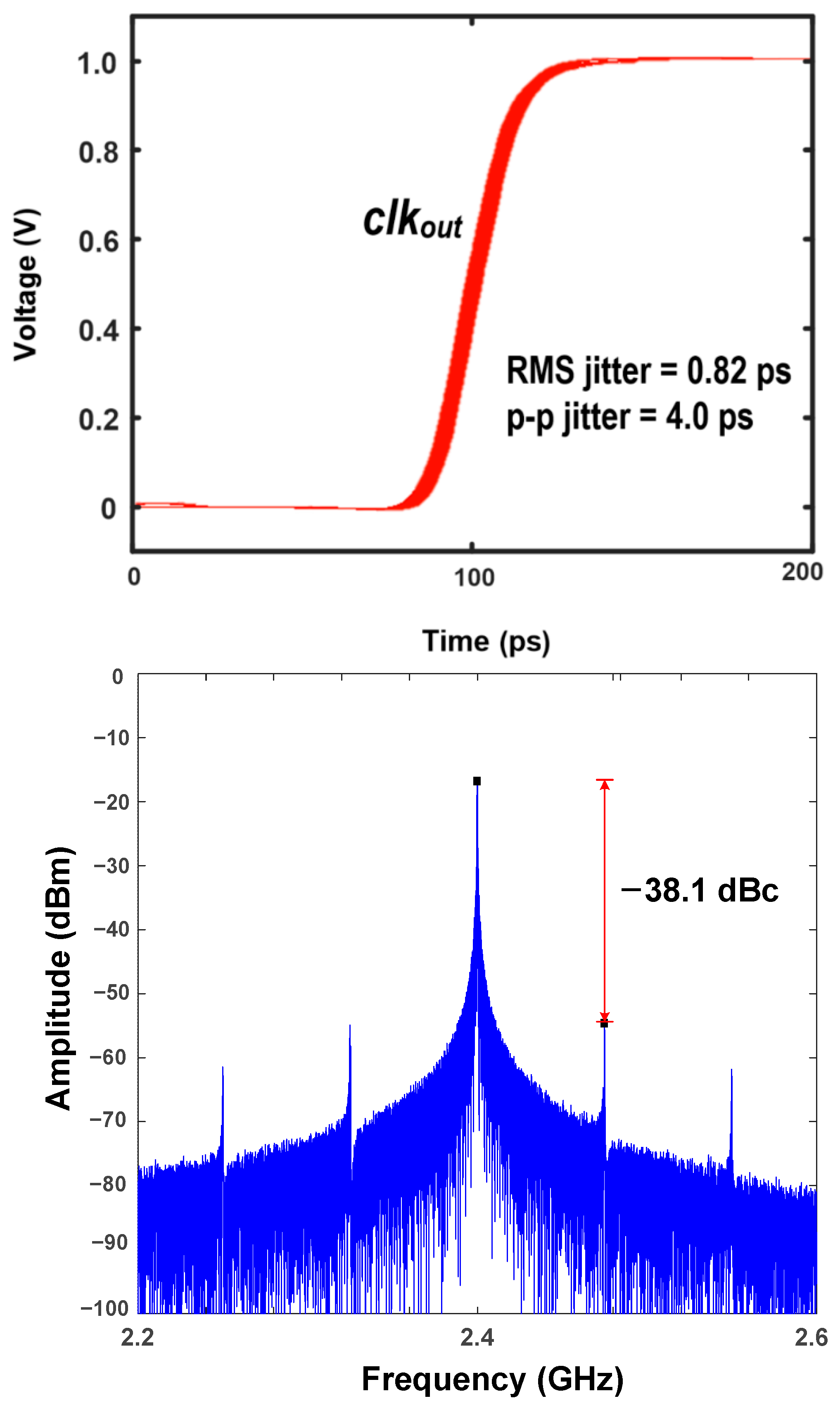
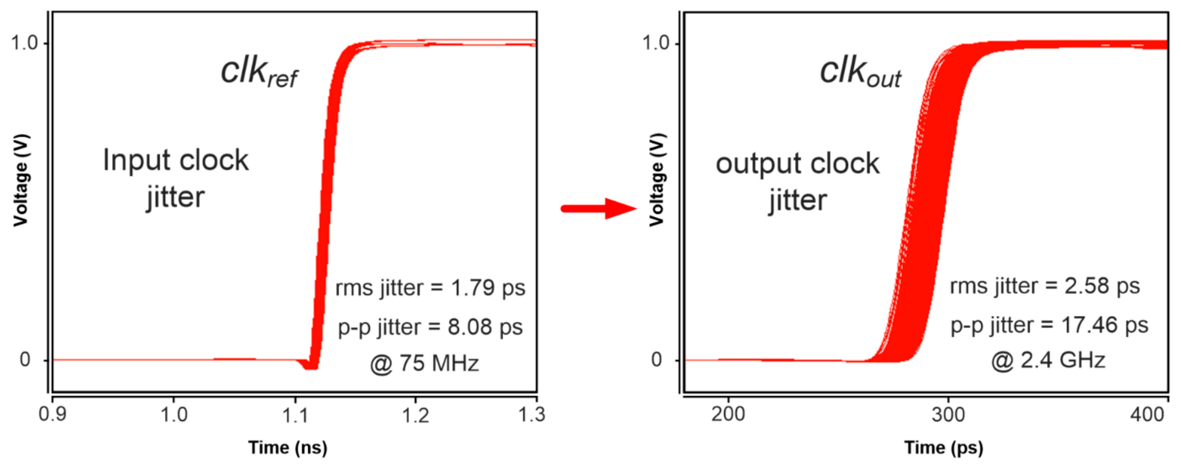
3. Experimental Results

The proposed MDLL has been implemented in a 65-nm CMOS process. Figure 6 shows the layout of the proposed MDLL core, where the active area is about 0.043 mm2. When the 75 MHz input reference clock is multiplied by N = 32 to generate an output clock of 2.4 GHz, the power consumption is about 3.3 mW from a 1.0 V supply.
Figure 7 shows the simulated locking process of the proposed all-digital offset-free cyclic Vernier-based MDLL. When the MDLL is enabled and the TDC starts operating at 160 ns, the initial phase error (=∆t) is about 2.9 ns. Since each TDC search process takes three reference clock cycles, the 10-bit output value of the DLF, LF [15:6], is changed at every three reference clock cycles. After five TDC search operations taking 15 reference clock cycles, the phase error becomes less than 2.3 ps, and the MDLL starts the sequential tracking mode. At this point, the MDLL is phase-locked, the TDC is turned off, and the BBPD and DSM are turned on to maintain the lock state.
Figure 8 shows the simulated jitter and reference spur performances of the proposed fast-lock all-digital MDLL at 2.4 GHz (N = 32). It achieves a root-mean-square (RMS) jitter of 0.82 ps and a peak-to-peak (p-p) jitter of only 4.0 ps. It also achieves a reference spur of −38.1 dBc. As shown in Figure 9, with an intentionally injected 8.08 ps p–p input clock jitter noise, the proposed MDLL obtains a 17.46 ps p–p (RMS jitter = 2.58 ps) output clock jitter. This means that even when input noise is injected, the effective p–p jitter is only 9.38 ps (=17.46 ps − 8.08 ps). Table 1 compares the performance of the proposed MDLL with previous digital MDLLs. Among the digital MDLLs, the proposed MDLL has the fastest locking time of less than 15 reference clock cycles, which is suitable for use in energy proportional serial link applications.

4. Conclusions

In this paper, we presented a new all-digital MDLL-based clock multiplier that features a cyclic Vernier TDC to achieve a fast lock capability of less than 15 reference clock cycles. This is the first fast-lock MDLL that utilizes a cyclic Vernier TDC to achieve both a wide phase detection range and high time resolution. In addition, the proposed offset-free TDC adopts a correlated double-sampling technique to improve jitter performance by eliminating mismatch and offset problems. The proposed MDLL utilizes DSM-based sequential tracking mode to achieve low output clock jitter characteristics. Implemented in a 65-nm 1.0-V CMOS process, the proposed MDLL generates a 2.4-GHz output clock with a frequency multiplication factor N of 32. The simulated peak-to-peak jitter is about 9.4 ps at 2.4 GHz, where the power consumption is only 3.3 mW (=1.375 mW/GHz). The proposed MDLL clock multiplier is suitable for use in high-speed burst mode serial link applications for chip-to-chip communications that require fast power-on/-off characteristics.

Author Contributions

Conceptualization, J.K.; methodology, J.K. and D.P.; validation, J.K. and D.P.; formal analysis, J.K. and D.P.; investigation, J.K.; data curation, S.C.; writing—original draft preparation, J.K and D.P.; writing—review and editing, J.K.; supervision, J.K.; project administration, J.K.; funding acquisition, J.K. All authors have read and agreed to the published version of the manuscript.

Funding

This research was funded and conducted under the “Competency Development Program for Industry Specialists” of the Korean Ministry of Trade, Industry and Energy (MOTIE), operated by the Korea Institute for Advancement of Technology (KIAT). (No. N0001883, HRD program for N0001883). This work was also supported by National Research Foundation of Korea (NRF 2019R1A2C-1010017). The EDA tools were supported by IDEC.

Conflicts of Interest

The authors declare no conflict of interest.

References

  1. Leibowitz, B.; Palmer, R.; Poulton, J.; Frans, Y.; Li, S.; Wilson, J.; Bucher, M.; Fuller, A.; Eyles, J.; Aleksic, M.; et al. A 4.3 GB/s mobile memory interface with power-efficient bandwidth scaling. IEEE J. Solid State Circuits 2010, 45, 889–898. [Google Scholar] [CrossRef]
  2. Zerbe, J.; Daly, B.; Dettloff, W.; Stone, T.; Stonecypher, W.; Venkatesan, P.; Prabhu, K.; Su, B.; Ren, J.; Tsang, B.; et al. A 5.6Gb/s 2.4mW/Gb/s bidirectional link with 8ns power-on. In Proceedings of the 2011 Symposium on VLSI Circuits-Digest of Technical Papers, Honolulu, HI, USA, 15–17 June 2011; pp. 82–83. [Google Scholar]
  3. Hossain, M.; Aquil, F.; Chau, P.S.; Tsang, B.; Le, P.; Wei, J.; Stone, T.; Daly, B.; Tran, C.; Eble, J.C.; et al. A Fast-Lock, Jitter Filtering All-Digital DLL Based Burst-Mode Memory Interface. IEEE J. Solid State Circuits 2014, 49, 1048–1062. [Google Scholar] [CrossRef]
  4. Choi, W.S.; Anand, T.; Shu, G.; Elshazly, A.; Hanumolu, P.K. A burst-mode digital receiver with programmable input jitter filtering for energy proportional links. IEEE J. Solid State Circuits 2015, 50, 737–748. [Google Scholar] [CrossRef]
  5. Hanumolu, P.K.; Brownlee, M.; Mayaram, K.; Moon, U.K. Analysis of charge-pump phase-locked loops. IEEE Trans. Circuits Syst. I 2004, 51, 1665–1674. [Google Scholar] [CrossRef]
  6. Hekmat, M.; Aryanfar, F.; Wei, J.; Gadde, V.; Navid, R. A 25 GHz Fast-Lock Digital LC PLL With Multiphase Output Using a Magnetically-Coupled Loop of Oscillators. IEEE J. Solid State Circuits 2015, 50, 490–502. [Google Scholar] [CrossRef]
  7. Farjad-Rad, R.; Dally, W.; Ng, H.T.; Senthinathan, R.; Lee, M.-J.E.; Rathi, R.; Poulton, J. A low-power multiplying DLL for low-jitter multi-gigahertz clock generation in highly integrated digital chips. IEEE J. Solid State Circuits 2002, 37, 1804–1812. [Google Scholar] [CrossRef] [Green Version]
  8. Elshazly, A.; Inti, R.; Young, B.; Hanumolu, P.K. Clock multiplication techniques using digital multiplying delay-locked loops. IEEE J. Solid State Circuits 2013, 48, 1416–1428. [Google Scholar] [CrossRef]
  9. Kundu, S.; Kim, B.J.; Kim, C.H. A 0.2–1.45-GHz subsampling fractional-N digital MDLL with zero-offset aperture PD-based spur cancellation and in situ static phase offset detection. IEEE J. Solid State Circuits 2017, 52, 799–811. [Google Scholar] [CrossRef]
  10. Marucci, G.; Fenaroli, A.; Marzin, G.; Levantino, S.; Samori, C.; Lacaita, A.L. A 1.7 GHz MDLL-based fractional-N frequency synthesizer with 1.4ps RMS integrated jitter and 3 mW power using a 1b TDC. In Proceedings of the 2014 IEEE International Solid-State Circuits Conference Digest of Technical Papers (ISSCC), San Francisco, CA, USA, 9–13 February 2014; pp. 360–361. [Google Scholar]
  11. Nandwana, R.K.; Saxena, S.; Elshazly, A.; Mayaram, K.; Hanumolu, P.K. A 1-to-2048 fully-integrated cascaded digital frequency synthesizer for low frequency reference clocks using scrambling TDC. IEEE Tran. Circuits Syst. I 2017, 64, 283–295. [Google Scholar] [CrossRef]
  12. Kim, H.; Kim, Y.; Kim, T.; Ko, H.-J.; Cho, S. A 2.4-GHz 1.5-mW digital multiplying delay-locked loop using pulsewidth comparator and double injection technique. IEEE J. Solid State Circuits 2017, 52, 2934–2946. [Google Scholar] [CrossRef]
  13. Helal, B.M.; Straayer, M.Z.; Wei, G.Y.; Perrott, M.H. A highly digital MDLL-based clock multiplier that leverages a self-scrambling time-to-digital converter to achieve subpicosecond jitter performance. IEEE J. Solid State Circuits 2008, 43, 855–863. [Google Scholar] [CrossRef]
  14. Kim, J.; Han, S. A fast-locking all-digital Multiplying DLL for fractional-ratio dynamic frequency scaling. IEEE Tran. Circuits Syst. II 2018, 65, 276–280. [Google Scholar] [CrossRef]
  15. Park, D.; Kim, J. A low-jitter 2.4 GHz all-digital MDLL with a dithering jitter reduction scheme for 256 times frequency multiplication. IEICE Electron. Express 2020, 17. [Google Scholar] [CrossRef]
  16. Chiu, Y.-K.; Liu, S.-I. A PVT-tolerant MDLL using a frequency calibrator and a voltage monitor. IEEE Trans. Very Large Scale Integr. (VLSI) Syst 2019, 27, 2698. [Google Scholar] [CrossRef]
  17. Yang, S.; Yin, J.; Mak, P.-I.; Martins, R.P. A 0.0056-mm2 –249-dB-FoM all-digital MDLL using a block-sharing offset-free frequency-tracking loop and dual multiplexed-ring VCOs. IEEE J. Solid State Circuits 2019, 54, 88–98. [Google Scholar] [CrossRef]
  18. Levantino, S.; Marucci, G.; Marzin, G.; Fenaroli, A.; Samori, C.; Lacaita, A.-L. A 1.7 GHz fractional-N frequency synthesizer based on a multiplying delay-locked loop. IEEE J. Solid State Circuits 2015, 50, 2678–2691. [Google Scholar] [CrossRef]
  19. Ali, T.-A.; Hafez, A.-A.; Drost, R.; Ho, R.; Yang, C.-K. A 4.6GHz MDLL with −46dBc reference spur and aperture position tuning. In Proceedings of the 2011 IEEE International Solid-State Circuits Conference Digest of Technical Papers (ISSCC), San Francisco, CA, USA, 20–24 February 2011; pp. 466–467. [Google Scholar]
  20. Chan, A.H.; Roberts, G.W. A jitter characterization system using a component-invariant Vernier delay line. IEEE Trans. Very Large Scale Integr. (VLSI) Syst 2004, 12, 79–95. [Google Scholar] [CrossRef]
  21. Chen, P.; Chen, C.; Zheng, J.C.; Shen, Y. A PVT insensitive Vernier-based time-to-digital converter with extended input range and high accuracy. IEEE Trans. Nucl. Sci. 2007, 54, 294–302. [Google Scholar] [CrossRef]
  22. Yu, J.; Dai, F.F.; Jaeger, R.C. A 12-Bit Vernier Ring Time-to-Digital Converter in 0.13 μm CMOS Technology. IEEE J. Solid State Circuits 2010, 45, 830–842. [Google Scholar] [CrossRef]
  23. Park, Y.; Wentzloff, D.D. A Cyclic Vernier TDC for ADPLLs Synthesized from a Standard Cell Library. IEEE Tran. Circuits Syst. I 2011, 58, 1511–1517. [Google Scholar] [CrossRef]
  24. Lu, P.; Liscidini, A.; Andreani, P. A 3.6 mW, 90 nm CMOS gated-Vernier time-to-digital converter with an equivalent resolution of 3.2 ps. IEEE J. Solid State Circuits 2012, 47, 1626–1635. [Google Scholar] [CrossRef]
  25. Lu, P.; Wu, Y.; Andreani, P. A 2.2-ps two-dimensional gated-Vernier time-to-digital converter with digital calibration. IEEE Tran. Circuits Syst. II 2016, 63, 1019–1023. [Google Scholar] [CrossRef]
  26. Dudek, P.; Szczepanski, S.; Hatfield, J.V. A high-resolution CMOS time-to-digital converter utilizing a Vernier delay line. IEEE J. Solid State Circuits 2000, 35, 240–247. [Google Scholar] [CrossRef]
  27. Enz, C.; Temes, G. Circuit techniques for reducing the effects of op-amp imperfections: Autozeroing, correlated double sampling, and chopper stabilization. Proc. IEEE 1996, 84, 1584–1614. [Google Scholar] [CrossRef] [Green Version]
Figure 1. Typical multiplying delay-locked loop (MDLL) architecture.
Electronics 10 00177 g001
Figure 2. Initial phase error detection using a time-to-digital converter (TDC) in the proposed MDLL.
Electronics 10 00177 g002
Figure 3. Proposed fast-lock all-digital MDLL, (a) architecture, (b) operation mode.
Electronics 10 00177 g003aElectronics 10 00177 g003b
Figure 4. Proposed offset-free cyclic Vernier TDC.
Electronics 10 00177 g004
Figure 5. Operation process of the proposed TDC mode.
Electronics 10 00177 g005
Figure 6. Layout of the proposed fast lock MDLL core block.
Electronics 10 00177 g006
Figure 7. Simulated locking process of the proposed fast lock all-digital MDLL (@2.4 GHz, N = 32).
Electronics 10 00177 g007
Figure 8. Simulated output clock’s p-p/RMS jitter and reference spur characteristics of the proposed all-digital MDLL (@2.4 GHz, N = 32).
Electronics 10 00177 g008
Figure 9. Simulated output clock’s p–p jitter performance with an injected input clock noise (@2.4 GHz, N = 32).
Electronics 10 00177 g009
Table 1. Digital MDLL performance summary and comparison.
Reference[9][12][13][14]This Work
Process and Supply65 nm/1.2 V28 nm/1.0 V130 nm/1.2 V65 nm/1.1 V65 nm/1.0 V
Freq. range (GHz)0.2–1.452.41.60.7–2.02.0–3.0
Output freq. (GHz)1.42.41.62.02.4
Reference freq. (MHz)87.5755050075
Multiplication factor (N)163232N/M = 8/232
Locking time (cycles)N/A>6000N/A4015
p-p/RMS jitter (ps)N/A15.9/1.5311.1/0.9322/2.8617.46/2.58
Power (mW)8.0 @1.4 GHz1.51 @2.4 GHz9.2 @1.6 GHz3.31 @1 GHz3.3 @2.4 GHz
Active area (mm2)0.0540.0240.760.0190.043
Publisher’s Note: MDPI stays neutral with regard to jurisdictional claims in published maps and institutional affiliations.

