Article

Assessment and Improvement of the Pattern Recognition Performance of Memdiode-Based Cross-Point Arrays with Randomly Distributed Stuck-at-Faults

1
Unidad de Investigación y Desarrollo de las Ingenierías (UIDI), Facultad Regional Buenos Aires, Universidad Tecnológica Nacional (UTN-FRBA), Buenos Aires C1179AAQ, Argentina
2
Consejo Nacional de Investigaciones Científicas y Técnicas (CONICET), Buenos Aires C1425FQB, Argentina
3
Departament d’Enginyeria Electrònica, Universitat Autònoma de Barcelona, 08193 Cerdanyola del Vallès, Spain
4
Departament de Telecomunicació i Enginyeria de Sistemes, Universitat Autònoma de Barcelona, 08193 Cerdanyola del Vallès, Spain
*
Authors to whom correspondence should be addressed.
Electronics 2021, 10(19), 2427; https://doi.org/10.3390/electronics10192427
Submission received: 31 July 2021 / Revised: 10 September 2021 / Accepted: 29 September 2021 / Published: 6 October 2021
(This article belongs to the Special Issue RRAM Devices: Multilevel State Control and Applications)

Abstract

:
In this work, the effect of randomly distributed stuck-at faults (SAFs) in memristive cross-point array (CPA)-based single and multi-layer perceptrons (SLPs and MLPs, respectively) intended for pattern recognition tasks is investigated by means of realistic SPICE simulations. The quasi-static memdiode model (QMM) is considered here for the modelling of the synaptic weights implemented with memristors. Following the standard memristive approach, the QMM comprises two coupled equations, one for the electron transport based on the double-diode equation with a single series resistance and a second equation for the internal memory state of the device based on the so-called logistic hysteron. By modifying the state parameter in the current-voltage characteristic, SAFs of different severeness are simulated and the final outcome is analysed. Supervised ex-situ training and two well-known image datasets involving hand-written digits and human faces are employed to assess the inference accuracy of the SLP as a function of the faulty device ratio. The roles played by the memristor’s electrical parameters, line resistance, mapping strategy, image pixelation, and fault type (stuck-at-ON or stuck-at-OFF) on the CPA performance are statistically analysed following a Monte-Carlo approach. Three different re-mapping schemes to help mitigate the effect of the SAFs in the SLP inference phase are thoroughly investigated.

Graphical Abstract

1. Introduction

Artificial neural networks (ANNs) have demonstrated outstanding results in the field of pattern recognition [1]. In this particular domain, the matrix-vector multiplication (MVM) method plays a key role, being the most computationally expensive operation during the classification phase. When implemented in CMOS-based platforms, MVM becomes costly in terms of power consumption and latency. As no drastic performance improvements can be expected from further technology scaling [2], alternative approaches involving novel technologies are being extensively researched worldwide. Among them, Resistive random access memory (RRAM) or memristor-based cross-point Arrays [3,4,5,6] (CPA, see Figure 1a) have demonstrated enormous potential in boosting the speed and energy efficiency of next-generation computing systems [7]. Moreover, the CPA structure can be scaled down to 4F2, F being the feature size of the technology node [8], which enables the large-scale integration of memory units.
The resistive switching (RS) mechanism is the physical phenomenon behind RRAM devices. It involves the creation (electroforming event) and the alternate rupture (RESET event) and completion (SET event) of a conductive filament (CF) spanning across the insulating layer in a metal-insulator-metal (MIM) structure. In the case of conductive bridge RAMs (CBRAM) and oxide RAMs (OxRAM), RS relies on the displacement of metal ions/oxygen vacancies within the dielectric film originating from the application of an external electrical stimulus [9,10]. For a fully formed CF, the device is in a low resistance state (LRS, often exhibiting a linear I-V relationship), whereas rupture of the CF leads to a high resistance state (HRS, usually showing a linear-exponential I-V dependence [9,10]). Voltage-controlled redox reactions occurring inside the insulator modulate the CF conducting properties in between these two limits, thus rendering intermediate states. This behaviour is schematically represented in Figure 1b. From the modelling viewpoint, the compact model originally proposed by Miranda [11] and later extended by Patterson et al. [12] is able to describe not only the LRS and HRS I-V loops but also the intermediate states, as well as the gradual transitions occurring in bipolar resistive switches. This is accomplished by considering a nonlinear transport equation based on two identical opposite-biased diodes in series with a resistor, as shown in the left inset of Figure 2a. Given that the resulting I-V relationship resembles a diode with memory, this device was named the quasi-static memdiode model (QMM).
Memristor-based CPAs for pattern classification have been studied in previous works using computer simulations relying on different memristor models and array architectures [3,13,14]. Hu et al. [3] reported a simulation-based case study of a CPA for character recognition using two CPAs of 256 × 26 (i.e., 256 rows by 26 columns, totalling ~13k devices) to represent both the positive and negative synaptic weights using a Verilog-A nonlinear memristor model [15]. Aiming to reduce both the area and power consumption arising from having two CPAs, an alternative architecture was considered by Truong et al. [13] (64 × 26, ~1.6k devices) using the same memristive device model. This model was also successfully used for voice recognition using a set of CPAs, using up to ~2.5k memristors [14].
However, although providing excellent results, these approaches fail to provide a consistent framework for introducing some of the main challenges currently faced in the development of RRAM-based CPAs—fundamentally, those linked to the high manufacturing variability and the relatively low yield. Different faults can occur in memristor-based CPAs and they can be roughly split into two groups: hard faults and soft faults. Although the effects of soft faults, e.g., read-one-disturb and read-zero-disturb, can be easily minimized as the memristor’s resistance is still tuneable [16,17], hard faults such as stuck-at faults (SAFs) pose a serious limitation to CPA-based architectures. An SAF denotes a memristor with its conductance state fixed to a high (stuck-at-ON, SA1) or low (stuck-at-OFF, SA0) conductance value. SAFs can have their origin in the fabrication process, as well as in the intense utilisation of the device, and despite the inherent robustness of the neural networks to variations [18], they may largely degrade their expected inference accuracy. Since the conducting properties of a metal-oxide layer in an RRAM device are relatively sensitive to the oxide thickness and the electroforming method [19], it is hard to prevent the occurrence of SAFs [20]. For example, a 4-Mb HfO2-based RRAM test chip may contain around 10% of RRAM faulty devices [21], so this is far from being a minor issue.
The methods proposed to tolerate SAFs in CPAs include redundancy schemes [22] or analog error correction codes (ECC) [23], retraining of the neural network [18,24], and alternative mappings of the synaptic weights into the memristor-based CPA [22], each of them having pros and cons. For example, the first option brings inevitable hardware cost and power consumption, as it involves large routing overhead to control the individual access transistors. This severely limits its applicability to large networks. Concerning the second method, re-training of the neural network may be inefficient as the training of large networks is computationally expensive, not to mention that in hardware approaches, the limited write endurance of RRAM cells [25] can lead to an increasing number of RRAM cells with an SAF during the re-training procedure. Lastly, fault-tolerant mapping algorithms are an interesting approach as, in contrast to the previously mentioned options, they involve little or no hardware overhead nor the computational effort of retraining the whole network. Examples of these are the row-flip, row-permutation and value range transformations proposed in [18,26]. However, it is worth pointing out that such methods are normally studied in idealized scenarios and from a logical viewpoint. In a realistic environment, CPAs have practical limitations such as the line resistances between adjacent cells (RL), the resistance window of the devices (RON and ROFF), the device-to-device variability (D2D), as well as the inherent conducting features of CPAs such as the so-called sneakpath problem (see Figure 1a). Although the former refers to the increase in RL as the fabrication technology scales down [27,28], the latter relates to the non-negligible current flowing through unselected devices [28,29].
Accordingly, SPICE simulation (or any other specific simulator) appears to be the most suitable approach to realistically investigating the complete system (CPA with parasitics and control electronics) [3,13,14,25,30,31,32]. However, this approach is also constrained to the limitations of the memristor model and works well for small-sized memristor-based CPAs, given again the high computational requirements [33]. Thereby, great attention has been paid in the last years to achieving a simulation tool that is capable of modelling the wide spectrum of existing memristive devices [34]. This has resulted in a variety of models, including simple behavioural models [15,35], device-specific physical-phenomenological models [36], and general phenomenological models (Yakopcic [37], TEAM [38], VTEAM [39], and Eshraghian [40]). Nevertheless, these models usually rely on various internal equations or the introduction of artificial window functions in the memory equation (ME), which pose serious mathematical drawbacks and are the root of convergence problems [41]. In this regard, the closed-form expression for the I-V curve (continuous and differentiable) and the iterative nature of the state variable computation of the QMM makes it suitable for dealing with arbitrary input signals (continuous and discontinuous, differentiable and non-differentiable). Such is the case of its application to the realistic circuital modelling of CPA-based single and multi-layer perceptrons (SLPs and MLPs) involving thousands of devices intended for the classification of large pattern datasets, as recently demonstrated [28,42]. Although a much simpler approach than the more complex RRAM-based ANNs explored in the literature (MLPs, [43,44,45], convolutional neural networks [46] (CNNs), spike neural networks [47] (SNNs), etc.), SLPs still allow us to study and clarify the limitations of ANNs caused by parasitic effects and non-idealities occurring in the synaptic layers implemented with CPAs. However, to the best of the authors’ knowledge, the impact of SAFs in realistic simulations is still to be evaluated to fully address the applicability of CPAs for the implementation of SLPs.
In this paper, the impact of SAFs in ex situ-trained CPA-based ANNs intended for large dataset pattern recognition tasks is addressed within the framework of realistic SPICE simulations involving the QMM. By considering an SLP (as well as the case of an MLP) as a case study, and the classification of grayscale images of hand-written digits and human faces from two different datasets (MNIST [48] and Yale Face Dataset B [49], respectively) for benchmarking, we explore the SLP and MLP sensitivity to SAFs as a function of the CPA’s parameters (RL, CPA size, and mapping). Based on the obtained results, three different re-mapping algorithms for mitigating the impact of the SAFs on the inference accuracy are tested in an integral and realistic simulation environment. The rest of this paper is organized as follows: in Section 2 the available literature regarding the study of SAFs’ impact on RRAM-based ANNs and their possible mitigation is briefly reviewed. Section 3 describes the methods, essentially the QMM. Section 4 performs an exploratory investigation of the impact of SAFs on RRAM-based ANNs from the viewpoint of realistic electrical simulations, providing useful design considerations and trade-offs. Section 5 discusses the algorithms used for SAF mitigation and evaluates the obtained results. Finally, the conclusions of this paper are presented in Section 6.

2. Previous Related Works
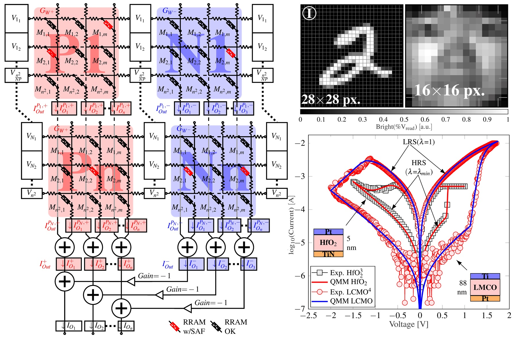
The impact of SAFs in RRAM-based ANNs has been addressed several times in the literature. Nevertheless, the vast majority of these research works (if not all of them) fail at some point to provide a realistic scenario for its study (that is, a SPICE simulation-based workflow using a realistic memristor model, capable of accounting for the CPA non-idealities) or they simply do not propose/test any mitigation technique. For instance, in Supplementary Table S1, we summarize 14 different works reported in the literature that do not meet these requirements, some of which are very detailed, comprehensive, and original research articles. In the following sub-sections we analyze in detail the work already done on this topic.

2.1. CPA Modelling

Very often, parasitic line resistances of the interconnecting lines in the CPA are completely ignored. In small CPA structures, and when considering thick, wide metal lines this approach may hold valid, as the resistance per unit length of such wordlines and bitlines are negligible (<1 Ω per square) when compared to the LRS resistance of the most potentiated RRAM device (around 1 kΩ). In such cases, the IR drop along the top and bottom lines of the CPA can be disregarded and it is correct to consider that the voltages applied to the wordline inputs are effectively delivered to all the RRAM cells. However, this is not valid for large CPAs or highly scaled metallic lines [27] (due to the size-dependent resistivity of Cu [50,51,52]), as the effects of the IR drops become notorious for the cells located away from the input terminals, resulting in a significant reduction of the voltage delivered to the cells located away from the input/output terminals. To the best of our knowledge, this is a limitation in the works of Mehonic et al. [53] (from 2019), Dias et al. [54] (2015), Zhang et al. [55,56] (2019), Xia et al. [22,26] (2017 and 2018), Woo et al. [57] (2020), Huang et al. [58] (2021), Yeo et al. [59] (2019), and Van Pham et al. [60] (2019).

2.2. Simulation Platform

Different approaches have been considered to investigate the performance of CPA-based neural networks but they are not suitable for every simulation scenario/analysis scope. For instance, some works address the problem from a logical/functional perspective, modelling the forward pass in each of the synaptic layers of the DNN simply as a mathematical matrix product between a vector of voltages and a matrix of conductances, which results in a vector of currents. This is the case for the works reported by Zhang et al. [55,56] (2019), simulated in C++ and MATLAB. Although such a CPA modelling and simulation platform allows one to deal with large fully connected (FC) and convolutional neural networks (CNNs) (and even more complex ANN architectures, such as the modified VGG-11 comprising 7.66 × 10⁶ synapses considered in the work of Xia et al. [26] (2017)), this approach is incapable of accounting for the electrical equivalent of the memristor-based CPA. Similar approaches have also been reported, considering a different simulation platform such as Python (Mehonic et al. [53] (2019) and Huang et al. [58] (2021)), but with similar limitations. Last but not least, neither C++, MATLAB, nor Python are circuit simulators, and therefore in a best-case scenario they are still limited to simulating only the CPA structure, and cannot deal with the CMOS blocks included in a typical RRAM neuromorphic circuit. In this context, the most suitable software for the electrical simulation of CPAs is SPICE (or any alternative language of this type), as it provides the versatility to add or remove parasitics by simply adding the required passive element to the CPA circuit netlist, while simultaneously supporting the simulation of the CMOS circuitry. Regarding the use of hardware approaches, although representing the most realistic scenario, they are costly and unpractical for the exploration of the wide parametric space of the CPA parasitics or RRAM characteristics. This is the case for the works by Chen et al. [21] (2015), Chen et al. [61] (2017), and Liu et al. [24] (2015).

2.3. RRAM Models

Regardless of the simulation platform considered and the realistic or idealized CPA modelling, a quite common weakness of many reported works is the over-simplified representation of the RRAM device. In the most unrealistic scenario, RRAM devices are modeled as a resistor of fixed value, which imposes a variety of limitations, perhaps the most important being: (i) such modelling is not capable of capturing the non-linearity of the RRAM devices (especially in the HRS regime), which may result in the under/overestimation of the device current [28]; (ii) it does not account for the SET/RESET transitions. This is the case for the works by Zhang et al. [55,56] (2019), Xia et al. [22,26] (2017 and 2018), Woo et al. [57] (2020), and Yeo et al. [59] (2019). As previously mentioned, given these boundary conditions, the most suitable simulation platform is SPICE. Nonetheless, there are different approaches in this regard, these being the use of behavioural and compact SPICE/Verilog-A models. The former are quite extensive and allow a very realistic formulation of the pinched I-V characteristics of memristive devices (see the works from Van Pham et al. [60] (2019), Cristiano et al. [62] (2018), and Romero et al. [63] (2019)), but this comes at the cost of increased computational requirements. Therefore, the latter are the most promising candidates for the simulation of large memristor-based ANNs. This was the type of model chosen in the work by Dias et al. [54] (2015).

2.4. Alternative RRAM Integration Structures

CPAs formed by memristors have drawn great attention due to the scaling properties of such structures (4F2). Nevertheless, they suffer from the so-called sneakpath effect, by which local current loops appear inside the CPA structure, producing errors in the total output current of each CPA bitline. Alternatives to this structure are the CPAs containing one transistor-one resistor (1T1R) structures. However, they have larger area requirements, which threatens the integration density achievable with simpler structures. 1T1R structures were investigated for the case of pattern recognition by Van Pham et al. [60] (2019) and Chen et al. [21] (2015) but considering a hardware approach. Another example is works by Cristiano et al. [62] (2019) and Romero et al. [63] (2019), in which the authors considered a 2T2R+3T1C structure and two pairs of conductances per synaptic weight, further compromising the maximum achievable integration density.

2.5. Costs Associated with the Mitigation of SAF Effects

Last but not least, it is worth mentioning that in five out of the 14 reviewed articles, no mitigation technique is discussed, showing that this is not the standard approach (Mehonic et al. [53] (2019), Dias et al. [54] (2015), Cristiano et al. [62] (2018), Chen et al. [21] (2015), and Huang et al. [58] (2021)). Another three articles consider re-training approaches to overcome the non-functional RRAM cells (Xia et al. [22] (2017), Yeo et al. [59] (2019), and Van Pham et al. [60]). This is an expensive approach in terms of computational complexity. However, most importantly, the repeated write cycles of the RRAM devices during the training loops also generate a new threat to the device endurance. Four additional works (Zhang et al. [55,56] (2019) and Xia et al. [22,26] (2017) and (2018)) discuss SAF mitigation techniques, but provide oversimplified CPA and memristor modelling approaches. Finally, another two works (Liu et al. [24] (2015) and Chen et al. [61] (2017)) tested mitigation techniques over a hardware CPA as a test vehicle. Although this is indeed the ideal study scenario, it is not capable of an exploratory analysis (CPA parameters are fixed). In summary, to the best of the authors’ knowledge, there are not many papers (if any) where the impact of SAFs on the performance of CPA-based SLPs is addressed in a full framework, comprising a standard circuit simulator with a realistic memristor SPICE compact model and considering different CPA non-idealities, and it is even less frequent to find cost-efficient SAF mitigation techniques evaluated within such frameworks.

3. Materials and Methods

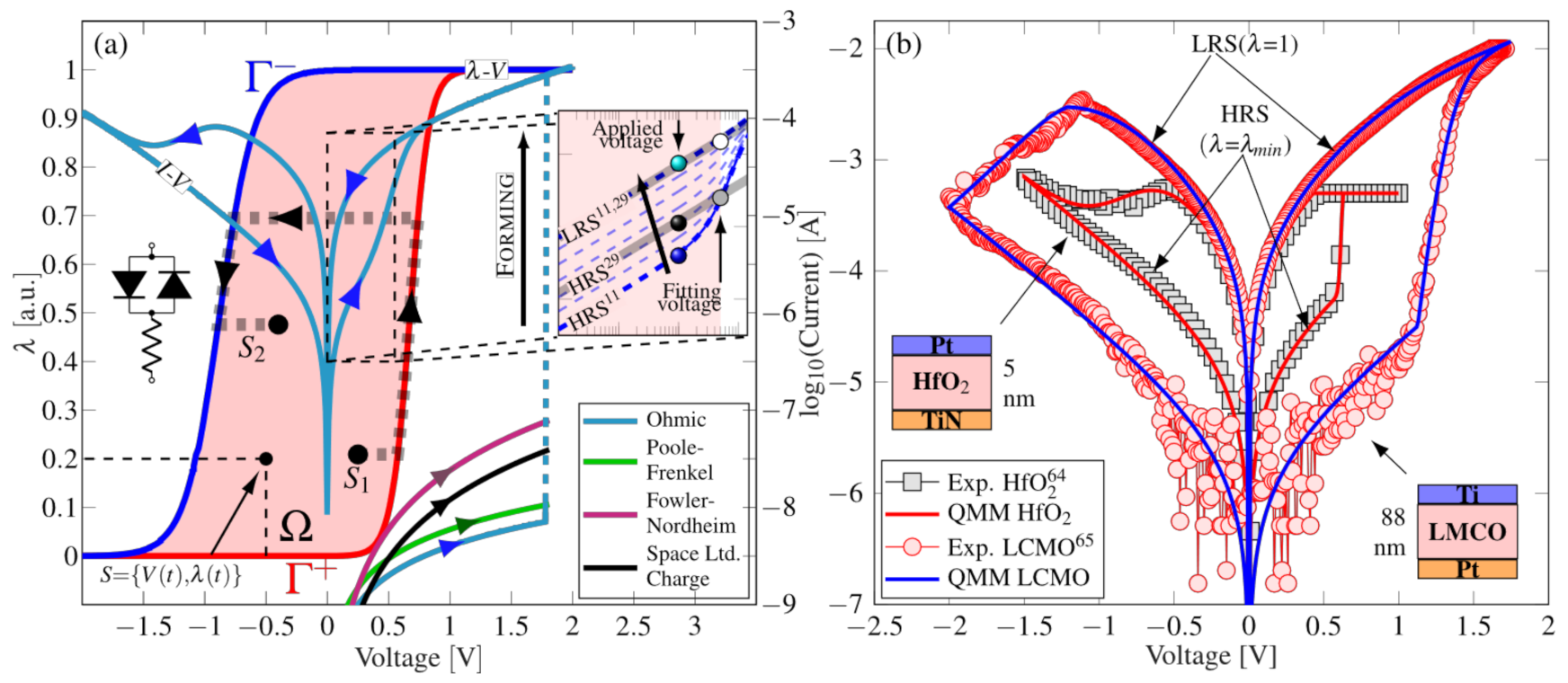
3.1. Quasi-Static Memdiode Model

Physically, the memristor is associated with a potential barrier that controls the electron flow in the CF. The conduction properties of this non-linear device change according to the variation of this barrier. Given the uncertainty in the area of the CF, the diode current amplitude is used as the reference variable instead of the potential barrier height. Following Chua’s memristive approach, the memdiode model comprises two equations, one for the electron transport and a second equation for the memory state of the device (ME), which is based on a hysteresis operator. The equation for the I-V characteristic of a memdiode is given by the expression:
I = s g n V W α R I 0 λ e α a b s V + R I 0 λ α R I 0 λ
where I0(λ) =Imin(1 − λ) + Imaxλ is the diode current amplitude, α is a fitting constant, and R is a series resistance. Equation (1) is the solution of a diode with series resistance and W is the Lambert function. Imin and Imax are the minimum and maximum values of the current amplitude, respectively. abs(V) is the absolute value of the applied bias and sgn() is the sign function. As I0 increases in Equation (1), the I-V curve changes its shape from exponential to linear through a continuum of states as experimentally observed for this kind of device. λ is a control parameter that runs between a lower limit λmin0 (setting the device in HRS), the exact value of which will be discussed below, and λmax1 (LRS) and is given by the recursive operator (Equation (2)):
λ V = m i n Γ V , m a x λ V , Γ + V
where min() and max() are the minimum and maximum functions, respectively, and   V is the voltage a timestep before V. The positive and negative ridge functions in Equation (2), Γ+(V) and Γ(V), represent the transitions from HRS to LRS (SET) and vice versa (RESET) and can be physically linked to the completion and destruction of the CF [9,10], respectively. They are defined by Equations (3) and (4):
Γ + V = 1 + e η + V V + 1
Γ V = 1 + e η V V 1
where η+ and η are the transition rates and V + and V the threshold voltages for SET and RESET, respectively. λ V   defines the so-called logistic hysteron or memory map of the device and keeps track of the history of the device as a function of the applied voltage (see the λ-V curve in Figure 2a). λ, calculated from Equation (2), yields the transition from HRS to LRS and vice versa through a change in the properties of the diodes depicted in the left inset of Figure 2a. The combination of Equations (1) and (2) results in an I-V loop such as that superimposed to the logistic hysteron in Figure 2a, which starts in HRS (λ = λmin) and evolves as indicated by the blue arrows printed on top.
The HRS (exponential) to LRS (linear) transition is detailed in the right inset of Figure 2a (solid blue lines), superimposed for comparison with a linear model [29], altogether with some intermediate states (dashed blue lines). It is clear that the memdiode model can accurately describe both HRS and LRS curves: as λ is swept from λmin (e.g., ~10−5) to 1, I0 in Equation (1) varies between Imin and Imax, gradually transitioning from linear-exponential to a linear regime as a consequence of a potential drop in series resistance. Additionally, this model can account for the transport mechanism in the pre-forming state, as well as the electroforming event. This is achieved by including two separate transport equations (namely, TEformed and TEfresh) and a second ridge function Γ f o r m + V , defined as per Equation (3) but in terms of η f o r m + and V f o r m + . The proposed model can be described by a simple HSPICE sub-circuit as shown in Supplementary Table S2. Fowler–Nordheim, Poole–Frenkel, or space-limited charge can be considered for the conduction mechanism through the pristine dielectric, but in this paper an ohmic I-V relationship was assumed for simplicity (see Figure 2a). The accuracy of the model is illustrated in Figure 2b by fitting experimental data corresponding to HfO2 [64] and LCMO [65] structures measured at room temperature (details of these samples can be found in Section S1.1 of the Supplementary Materials).

3.2. Procedure for SPICE CPA Creation, Training, and Simulation

The procedure originally proposed in [28] for creating and simulating the SLP or MLP used as case study is considered herein. The workflow is summarised in the chart depicted in Supplementary Figure S1a. The tasks can be split into two parts: on one hand the SLP creation, training, and circuit-representation SPICE code generation (MATLAB), and on the other the simulation (HSPICE). The structure of the resulting neuromorphic circuit is detailed in Section S1.2 in the Supplementary Materials, and a simplified circuit schematic is presented in Supplementary Figure S1b. For the study reported in this paper, two different databases are considered, the MNIST (see Supplementary Figure S1c) and Yale Face Database, the details of which are presented in Section S1.3 in the Supplementary Materials.

4. Results and Discussion

4.1. Impact of the CPA Parasitics on the Recognition Accuracy

Before analysing the impact of SAFs on CPA-based SLPs or MLPs, it is worth reporting the main effects of the CPAs’ non-idealities on the inference accuracy of the fault-free SLP. These are the resistance window amplitude (RON/ROFF), the device-to-device (D2D) variability, signal-to-noise Ratio (SNR) degradation, the presence of a non-negligible line resistance RL, and the influence of the image size, among others. For further details regarding these aspects, the reader is referred to the previous works by our group [28,42]. These were studied within the framework of CPA-based SLP creation, training, and SPICE simulation presented in Supplementary Figure S2, together with a simplified schematic representation of the generated SLP circuit. To account for the first issue (RON/ROFF ratio), 12 different model plays for the QMM with a variety of RON/ROFF ratios considered in the literature [43,44,45,66,67] were defined by (i) equally scaling the HRS and LRS curves by a factor of 10: A1 (ROFF~1 MΩ and RON~100 kΩ), A2 (~100 kΩ and ~10 kΩ), A3 (~10 kΩ and ~1 kΩ), and A4 (~1 kΩ and ~100 Ω); (ii) scaling the HRS curve by a factor 10 while keeping the LRS fixed: B1 (~1 MΩ and ~100 Ω), B2 (~100 kΩ and ~100 Ω), B3 (~10 kΩ and ∼100 Ω), and B4 (~1 kΩ and ∼100 Ω); and (iii) scaling the LRS curve by a factor of 10 while keeping the HRS curve fixed: C1 (~1 MΩ and 100 ~kΩ), C2 (~1 MΩ and ~10 kΩ), C3 (~1 MΩ and ~1 kΩ), and C4 (~1 MΩ and ~100 Ω). The corresponding I-V loops are shown in Supplementary Figure S2a–c. The RON/ROFF ratio’s influence on the inference accuracy was addressed by simulating a 784 × 10 SLP (using the original 28 × 28 px. MNIST images shown in Supplementary Figure S2d). Vread was set to 300 mV and RL was fixed to 2 Ω. For this case, the SAF ratio was kept equal to 0. The simulation results are presented in Supplementary Figure S2e,f, indicating an accuracy loss corresponding to the upward shift in the resistance window for model plays A1–A4 (constant RON/ROFF ratio) or the LRS curve for model plays C1–C4 (constant ROFF, increasing RON/ROFF ratio). On the contrary, model plays B1B4 (constant RON, decreasing RON/ROFF ratio) show a highly degraded accuracy that is almost independent of the model play considered. Therefore, the LRS characteristic (RON) has a major impact on the inference accuracy. Significant differences arise between A1–A4 and C1–C4 model plays when their sensitivity to D2D variations is introduced, as shown in Supplementary Figure S2g. In this scenario, the larger RON/ROFF ratio of the latter (particularly for C2–C4) allows one to minimise the susceptibility of the SLP-to-D2D variability.
The performance of the CPA-based SLP also depends on RL. As each memristor is in series connection with a number of RL resistors, the fraction of the voltage effectively delivered to the memdiode decreases as the ratio RL/RON tends towards unity, as shown in Supplementary Figure S2h, showing a common trend across the different C1–C4 model plays. Interestingly, when a smaller SLP is tested (64 × 10, using the MNIST images down-sampled to 8 × 8 px.) the same trend arises, but right-shifted. As the total resistance associated with the CPA wires is proportional to the CPA size, it is expected that downsizing the input patterns would boost the recognition accuracy. Nevertheless, when the resolution of the MNIST images is reduced below 12 × 12 px. the digit becomes practically illegible for the human eye (see Supplementary Figure S2d), indicating a trade-off between legibility and the voltage drop that defines the optimum size of the SLP for a given set of RON, ROFF, and RL values (see Supplementary Figure S2i). Supplementary Figure S2i also shows a reduced RL dependency for smaller SLPs (i.e., CPAs with fewer devices) than in their larger counterparts. The realisation of larger CPAs by considering smaller partitions is shown to efficiently improve the inference accuracy [27,28,68]. Note that for this latter analysis, only model play C2 was considered. This is because this model play provides the best trade-off between SNR, inference accuracy, and tolerance to D2D variations. Model play C1, for instance, has a poor SNR as the high values of RON and ROFF produce extremely low operating currents (see Supplementary Figure S2j).

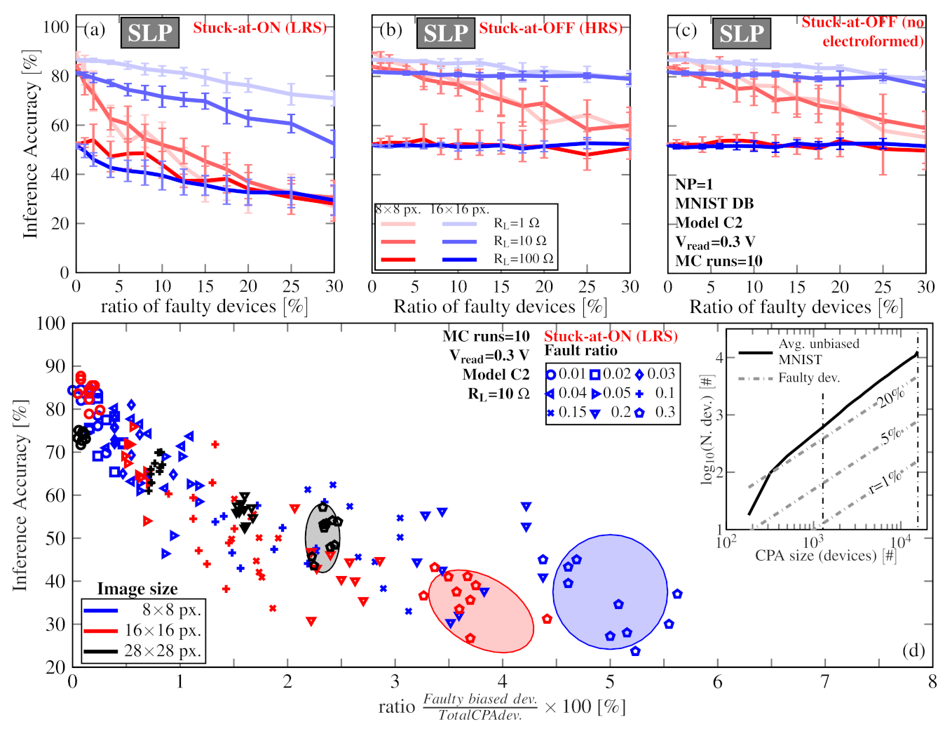
4.2. Impact of the Fault Ratio on the Inference Accuracy

Stuck-at faults cause the unwanted potentiation (SA1, device stuck at LRS) or depression (SA0, device stuck at HRS, or even not electroformed) of synaptic connections in the CPA [22,56]. In this paper, the inference accuracy is studied for both cases, also accounting for possible non-electroformed devices (SA0_nE). The memristor model considered here is particularly suitable for injecting such faults as it can be achieved by varying one single parameter: λ (λ = 1 corresponding to SA1 faults, λ = λmin to SA0 faults, and λ = 0 to SA0_nE faults). Given the stochastic nature of the spatial distribution of SAFs across the CPA [21,69], Monte Carlo (MC) simulations of the CPA were performed, assuming different ratios of faulty devices (FD ratio). In each MC run, faulty devices are randomly injected following a uniform distribution [22,69] into the CPA and, subsequently, the defective CPA is used to classify the images from the MNIST dataset. Faults are directly injected into the conductance matrices G M + and G M (see the flowchart in Supplementary Figure S1a). The obtained inference accuracy is then averaged among all MC runs for a given FD ratio and presented in Figure 3. The inference accuracy for the three SAF cases are presented as a function of the FD ratio for two image sizes (8 × 8 px. and 16 × 16 px.), different values of RL (1 Ω, 10 Ω and 100 Ω), and considering model play C2 (See Supplementary Figure S3c). To minimise the impact of series resistance, for both the SLPs used to classify the 16 × 16 px. images and the MLPs studied, we have considered the use of small partitions (8 blocks in the SLP—4 for the positive synaptic weights and 4 for the negatives—and 30 in the MLP). For the SLP considered for the 8 × 8 px. no partitioning was considered given the rather small size of the crossbars involved. Different normalisation methods (NM) used to map W M to G M + and G M were tested in terms of robustness against SAFs and their impact on the inference accuracy. Ten MC runs were considered for each combination or RL, NM, image size, and FD ratio, totalling ~4.3k simulation runs.

4.2.1. Impact of the Normalisation Method (NM)

The elements of W M are in the range m i n W M , m a x W M and follow the distribution shown in Figure 3a. In order to be mapped to a conductance level in the range G H R S , G L R S , they must be normalised first to the range 1 , 1 . Usually [18,70], this normalisation is achieved by dividing W M by the absolute value of the maximum element in W M (normalisation method 1, NM-1) or by measuring the maximum difference between elements in W M (NM-2). As expected, the normalised W M matrices W M N 1 and W M N 2 preserve the exact same distribution and m a x W M / m i n W M ratio, as shown in Figure 3b,c, respectively. Interestingly, for the case of the MNIST images resized to 8 × 8 px., which were used for benchmarking in this work, ~95% of the elements from W M N 1 fall within the range [−0.5,0.5], with this ratio reaching ~99% when considering W M N 2 . This implies two major drawbacks: first, neither NM-1 nor NM-2 exploits the entire dynamic range of the memristors, as most of the devices will be set in a conductance value in the range G H R S , G L R S + G H R S / 2 . Second, the concentration of synaptic weights close to 0 ( G H R S ) exacerbates the impact of the SA1 faults, as indicated by the SWV metric [24]: as a significant fraction of the devices are mapped close to G H R S (thereby λ→λmin) an SA1 fault (λ=1) causes a significant departure from the target conductance, thus increasing SWV and degrading the inference accuracy. In order to mitigate both problems, an alternative approach (NM-3) based on the Gaussian-like distribution of the elements of W M is proposed in this work. In this context, an element w i , j W M has a probability Pi of being within the range μ W M ± i σ W M , where μ W M and σ W M   are the mean and standard deviation of the values of W M . For i values ranging from 1 to 4, ~68.3%, ~95.5%, ~99.7%, and ~99.9% of the synaptic weights will be within this range, respectively [71]. Thus, values exceeding such limits are set as equal to μ W M ± i σ W M and then W M is normalised to obtain W M N 3 . The histograms for the elements in W M N 3 are presented in Figure 3d–f for 2, 3, and 4 σ W M , respectively.
The impact of the NM on the inference accuracy as a function of the FD ratio is presented in Figure 3g–I, considering SA1, SA0 and SA0_nE faults. RL was set to 10 Ω in all cases. As reported in the literature [45,53], SA1 faults have a much more significant impact on the inference accuracy than SA0 faults. Little, if any, difference exists between the SA0 and SA0_nE cases. A major influence of NM on the inference accuracy as a function of the FD ratio can be observed in Figure 3g for the case of injecting SA1 faults, with NM-3 showing the highest robustness against this kind of SAF. Unlike the rapid accuracy loss observed as the FD ratio increases for NM-1 and NM-2, the NM-3 cases have a greater tolerance to faulty devices. In fact, the more W M N 3 departs from a Gaussian-like distribution, the smaller the impact of the FD ratio on the inference accuracy (see the difference between NM-3 with 2 σ W M   and with 4 σ W M ). Nevertheless, this improvement comes at the cost of a higher power consumption (reaching roughly ~10 mW in an SLP comprising ~15.6k synapses) during the inference phase (see the inset of Figure 3h) and a slightly lower accuracy in the fault-free scenario (see the inset of Figure 3i). The increase in the power consumption is an expected side-effect of mapping a larger fraction of the W M elements closer to G L R S , which inevitably increases the currents flowing through the CPAs. This also plays a role in the lower accuracy observed for higher values of RL in the fault-free SLP (inset of Figure 3i), which could be regarded as an increase in the RL/RON ratio. Moreover, even for reduced values of RL, there is a sensible accuracy degradation caused by the re-distribution of the synaptic weights from W M to W M N 3 . Thereby, NM-3 is considered from here on, as it provides the highest robustness against SAFs and the lowest accuracy loss in the fault-free scenario.
The differing robustness demonstrated against SAFs, when considering SA1 or SA0 faults, can be attributed to the distribution of the synaptic weights (see Figure 3a–f). Note that not only are SA1s more problematic than SA0s in terms of the accuracy degradation (as can be seen in Figure 2g and Figure 3h), but the CPA sensitivity to SA1 also increases as the synaptic weights to be mapped in the CPA are increasingly concentrated around λ = 0 (that is, mapped close to an HRS). As previously mentioned, the higher the concentration of synaptic weights to be mapped close to an HRS, the higher the chance that an SA1 affects a device, which in a fault-free scenario would be mapped to an HRS, thus causing a significant departure from the target synaptic weight. In a similar fashion, but with the opposite outcome, a large concentration of devices being mapped to an HRS increases the probability that an SA0 will affect a device which in a fault-free scenario would be mapped to an HRS. However, in such a situation, the error induced is minimal.
For the sake of completeness, it is also worth discussing the case of considering the combination of SA0 and SA1 in the CPAs, assuming different ratios. In this regard, the inference accuracy as a function of the ratio of SA1s with respect to the total number of SAFs is shown in Figure 3j (note that in the top axis, the equivalent ratio of SA0 faults with respect to the number of SAFs is indicated). The ratio of SAFs was swept parametrically, resulting in six different scenarios: the ratios of SAFs are assumed to be 5%, 10%, 15%, 20%, 25%, and 30%. Note that as this ratio increases from 5% to 30%, the accuracy trends are downshifted, while keeping a common feature—for a given ratio of SAFs, as the SA1 faults become dominant when compared to their SA0 counterparts, the inference accuracy gradually decreases, and the extreme cases can be studied in detail in Figure 3g–i.
Last but not least, the sensitivity of SAFs with different normalisation methods is considered for the case of an MLP. In this case, we have assumed the MNIST images are rescaled to 8 × 8 px, and we classified them using an MLP with a 64 × 54 × 10 structure. The first synaptic layer (64 × 54) is divided into 12 partitions (totalling 24 partitions if we consider the positive and negative synaptic weights), each of size 16 × 18, and the second into three partitions (18 × 10), and the same memristor model play and line resistance are assumed (C2 and RL = 10 Ω). The simulation results show that similar trends to the SLP case are obtained, showing a higher sensitivity to the SA1 faults in comparison with the SA0 faults. There is also a higher sensitivity to both SAFs when comparing these trends to those obtained for the SLP case. This can be attributed to the fact that the second (and following layers) not only induce errors in the output vector produced by the MVM operation, but also receive an erroneous input vector caused by the errors introduced by the previous layers. Finally, an increase in the ANN robustness by considering an alternative normalisation method is also observable for this scenario. Note that NM-3 achieves a more robust mapping, as was also observed in the SLP scenario.

4.2.2. Influence of the Line Resistance (RL) and Image Size (n × n)

The inference accuracy vs. FD ratio was also studied for different RL values (1 Ω, 10 Ω and 100 Ω) and MNIST image sizes (8 × 8 px. and 16 × 16 px.). In both cases, the inference accuracy for FD ratio→0 is down-shifted as RL increases [28] from 1 Ω to 100 Ω, in agreement with the results shown in Supplementary Figure S2i. For the smaller images (8 × 8 px., SLP of size 64 × 10) and regardless of the SAF mode, the inference accuracy sensitivity on the FD ratio notably increases as RL decreases, which is most notable for the 1 Ω case, as illustrated in Figure 4a–c. Interestingly, for the SA0 faults, the inference accuracy becomes insensitive to the FD ratio for the maximal RL (100 Ω), as expected for a lower SWV metric [24]. When addressing the 16 × 16 px. MNIST images, very similar trends can be observed, but with a shallower dependence on the FD ratio. For comparison purposes, such trends are superimposed onto the previous ones in Figure 4a–c. Note that for the classification of the 16 × 16 px. MNIST images, the inference accuracy already becomes insensitive to the FD ratio for RL = 10 Ω if SA0 faults are injected.
This behaviour can be ascribed to the combination of two factors. On the one hand, it has been shown in the literature [27,28,29] that the CPA’s read margin (RM, that is, the fraction of the applied input voltage (Vread) effectively delivered to the memory cells (Vcell), i.e., Vcell/Vread) is jointly determined by RL and the memristor resistance (Rmemd, which varies between ROFF and RON). In a very basic analysis, each memristor is part of a conductive path between the CPA’s input wordline i and output bitline j. For an N × M SLP, the average parasitic resistance associated with this path is RL[(N + M)/2 + 1] [28,45]. Within this simplified scenario, the Vcell/Vread ratio could be obtained from the voltage divider between Rmemd and RL[(N + M)/2 + 1]. The calculated values are shown in Table 1 for the two image sizes and different RL values, considering both SA0 and SA1 faults. Despite being a limitation when attempting to improve the inference accuracy in fault-free CPAs, the observed reduction of RM as RL increases has a positive side effect when considering SAFs as it results in lower voltages applied to defective devices. This is particularly noticeable for the case of SA1 in the 256 × 10 SLP used to classify the 16 × 16 px. MNIST images: only ~49% of the input voltage is applied to the faulty devices, which thereby reduces their contribution to the bitline output current in roughly the same amount.
On the other hand, images from MNIST-like datasets [28] include a fraction of inactive pixels (for example, those close to the image borders). Interestingly, this ratio does not hold as the images are downscaled, as visually represented in Supplementary Figure S2d. Instead, smaller images have a lower ratio of inactive pixels. Thereby, when presenting the inputs of a faulty n2 × M SLP with the n × n test images, the fraction of unbiased RRAM cells in the CPA is found to increase with n. This is shown in the inset of Figure 4d. It can be seen that the number of unbiased devices in the CPA exhibits a steeper increase than the number of faulty devices for 1%, 5%, and 20% FD ratios. As the faulty devices are distributed uniformly all over the CPA, it is reasonable to expect that in a large CPA, a significant fraction of the faulty devices are unbiased and therefore play no role in the inference stage. To test this interpretation, the raw data (that is, the inference accuracy calculated in each MC run) obtained for RL = 10Ω from Figure 4a were represented in the scatterplot from Figure 4d as a function of the ratio of biased faulty devices (BFD ratio). For the sake of completeness, the full-sized 28 × 28 px. images were also included. The total number of synapses in the simulated SLP sizes are 1280 sys. (8 × 8 px. images (blue markers)), 5120 sys. (16 × 16 px. (red markers)), and 15,680 sys. (28 × 28 px. (black markers)). Two relevant observations can be made regarding Figure 4d: first, despite the clearly different trends exhibited in Figure 4a for the 8 × 8 px. and 16 × 16 px. image cases, a common overall behaviour is observed when considering the inference accuracy vs. the BFD ratio for multiple SLP sizes. Second, only a fraction of the faulty devices is effectively biased, and this fraction decreases as the CPA becomes larger (the case of 30% of faulty devices has been shaded as a guide to the eye).

5. CPA Remapping Procedures

The ideal mapping of synaptic weights to conductances [18,70] (see Section S1.2 in the Supplementary Materials) can be altered in order to minimise the impact of SAFs. In this connection, three different approaches, described through Section 5.1, Section 5.2 and Section 5.3, are explored in this work. They all rely on two premises: (i) that the locations of the faulty devices are known, and (ii) that rows in the weight matrix can be permuted (electrically re-addressed). On one hand, and concerning point (i), in [72] the authors presented a simple method to test the switching activity in the CPA and thereby to easily obtain the spatial location of the SAF devices in the CPA. On the other hand, the order of the rows and columns in a matrix can be permuted without changing the final result of a matrix-vector multiplication if the order of the inputs and outputs are simultaneously permuted [56]. The three algorithms discussed are based on: (i) the compensation of the defective cell in a dual CPA scheme, (ii) the minimisation of the sum weight variation, and (iii) the mean-bias-dependent mapping of the image pixels. It is worth noting that although similar approaches have been discussed in the literature, they have always been addressed towards oversimplified modelling of both the CPA and the RRAM device (assuming no line resistance, linear devices, and providing no details of the simulation procedure).

5.1. Algorithm 1: Fault-Tolerant Adaptative Mapping

In this paper, and as in many previous studies [3,22,68,73], two memristors are used to represent each element of the weight matrix. Furthermore, as mentioned in the Supplementary Materials in regard to the simulation method (see Section S1.2 in the Supplementary Materials), WNorm is computed as WNorm+WNorm, with WNorm+ and WNorm being the positive and negative elements of WNorm, respectively. This technique allows one to implement a simple yet powerful remapping procedure to minimise the impact of SAFs. This implies that for a given faulty RRAM cell in the positive (negative) CPA denoted as g i , j + , the corresponding RRAM cell in the negative (positive) CPA g i , j + is tuned so as to compensate the error in g i , j + . This can be summarised as follows (see Equation (5)):
g i , j + = g i , j + ,   |   w M N o r m + w M N o r m     a r e   f a u l t - f r e e g i , j + g i , j +   |   w M N o r m + w M N o r m     a r e   f a u l t - f r e e
For example, if the target weight ( w M N o r m ) is positive but the corresponding RRAM cell in the positive crossbar ( w M N o r m e f f + ) contains an SA1 fault, an error occurs with the original mapping method because the positive RRAM cell cannot be tuned to the target value. Since the positive cell is stuck at the highest value, w M N o r m is realized by increasing the conductance of the corresponding RRAM cells in the negative CPA. Nevertheless, it is worth noting that the direct application of Equation (5) to mitigate the effect of faulty devices may result in non-realisable synaptic weights. For example, for a positive target value which is to be realized with a fault-free memristor in the positive CPA and SA1 device in the negative CPA, Equation (5) would indicate a corrected weight for the positive memristor larger than 1. Therefore, certain faults can be tolerated by the direct application of the method denoted as (recoverable faults), whereas others require further processing as (unrecoverable faults), as shown in Table 2. Note that recoverability of a given combination of a fault-free/faulty pair of memristors depends on the polarity of the synaptic weight to be represented. Let us consider, for instance, the case of an SA1 fault in the g i , j + memristor, whereas consider the g i , j memristor to be fault-free. In this case, if the synaptic weight associated with that element ( w i , j ) is positive, then the fault is recoverable, as g i , j can be tuned to compensate for the excess in g i , j + caused by the SA1 fault. On the contrary, if w i , j is negative, the fault is unrecoverable, given that g i , j should be increased beyond LRS (λ > 1) to compensate for the SA1 fault in g i , j + .
By means of an iterative-row permutation algorithm, unrecoverable faults can be turned into recoverable faults, as depicted in Figure 5a. Note that, as an example, the {i,j} and {k,l} row pairs are permuted, which allows one to turn unrecoverable faults in g i , 1 + , g j , 1 + , g k , 1 , g l , 3 (Figure 5a, top) into recoverable faults (Figure 5a, bottom). The complete re-mapping procedure, including the row permutation and conductance compensation, is presented in pseudo code in Algorithm 1.
Algorithm 1: Fault-tolerant adaptive mapping
Electronics 10 02427 i001

5.2. Algorithm 2: SWV-Minimisation-Based Row Permutation

Let the weight variation (WV) be equal to w i , j S A F w i , j , where w i , j S A F is a synaptic weight in the faulty weight matrix W M N o r m S A F and w i , j is the corresponding synaptic element in the fault-free weight matrix W M N o r m . Then, the metric referred to as the sum weight variation (SWV) [24] can be derived in order to quantify the deviation of the W M N o r m S A F matrix from the fault-free W M N o r m matrix and it is computed as indicated by Equation (6):
SWV = i = 1 M j = 1 N w i , j e f f w i , j
where M and N stand for the number of rows and columns of W M N o r m . From Equation (6), it can be noted that the lower the value of SWV, the lower the impact of the SAFs on the mapped weight matrix. The proposed algorithm therefore consists in minimizing SWV by performing a sequential row permutation until reaching the minimum possible value of SWV. This approach is illustrated in Algorithm 2.
Algorithm 2: SWV-minimisation-based row permutation
Electronics 10 02427 i002

5.3. Algorithm 3: Mean-Bias-Dependent Mapping

As shown in Figure 5b (top) for the MNIST characters resized to 12 × 12 px., a considerable number of pixels remain black (inactive) whereas some others are normally white (active), regardless of the digit being considered. As we are encoding the pixel brightness as a voltage value ranging from 0 to Vread, we can obtain the mean brightness (voltage) for each pixel in the MNIST dataset. These two cases have been exemplified in Figure 5b: pixel i stands for a normally inactive pixel (e.g., pixels close to the image borders), whereas pixel j indicates a normally active pixel (e.g., a pixel located in the centre of the image). For the 12 × 12 px. image-size case, each of the resulting 144 px. is used to bias each of the rows in two (positive and negative weights) 144 × 10 CPAs. In the simplest possible scenario, the 1st pixel (the upper-left corner of the MNIST images) would be mapped to the 1st CPA row. Then the ith pixel would be mapped to the ith row, the jth pixel to the jth row, and lastly the 144th pixel (lower-right corner of the MNIST images) to the 144th row. Nevertheless, such mapping does not take into account the distribution of the faulty devices in the CPA. Knowing their spatial distribution, it is possible to determine how many faulty devices are connected to each CPA row, and then re-map the most active pixels to the ”less faulty” rows (rows with lower numbers of connected faulty devices) and the inactive pixels to the faultiest rows. This re-mapping procedure is schematically depicted by the row permutation in Figure 5b (bottom) for pixels i and j and in Algorithm 3.
Algorithm 3: Mean-bias-dependent mapping
Electronics 10 02427 i003

5.4. Performance of the CPA-Remapping Algorithms

From the results presented in Section 4.1 and Section 4.2, it is evident that SAFs (both SA1 and SA0 faults) have a non-negligible impact on the classification accuracy of the SLP, regardless of the normalisation method, image size, and RL/RON ratio considered. In this regard, techniques to help tolerate such faults are required to enable the reliable operation of CPA-based SLPs. Three different approaches were proposed in Section 5.1, Section 5.2 and Section 5.3, defined as re-mapping Algorithms 1–3, and their capability to mitigate the impact of SAFs is tested in this Section. Two possible scenarios are assumed. First, the classification of the 8 × 8 px. MNIST images by a partitioned (number of Partitions, NP=4, for each polarity of synaptic weights) 64 × 10 SLP is considered, as this case shows the highest sensitivity to SAFs in Figure 4. Second, a different image dataset was taken into account to provide a more representative test of the proposed algorithms. In this way, images from Yale Face Dataset B were downscaled to a 16 × 16 px. resolution and classified by means of a 256 × 38 SLP, where each of the G M + and G M matrices are implemented by four (NP=4) 64 × 38 CPAs. Some image samples in this dataset are shown in Figure 6a. As for the previous simulations, the I-V characteristics of the memristors were represented by model play C2, RL was set to 10 Ω, G M + and G M were obtained by NM-3, and 10 MC runs were performed for each FD ratio. Note that only SA1 and SA0 cases were considered, given the very similar outcomes of SA0 and SA0_nE presented in Figure 3 and Figure 4. In addition, the study is presented in terms of the extreme case of having only SA1 or SA0 faults, as assessing the combined effect of both would require multiple scenarios with different ratios of SA1 to SA0 faults. Finally, simulations (i)–(iv) are performed for a given kth sample of complete randomly distributed SAFs: (i) original mapping; (ii)–(iv) the fault-free cells are tuned based on Algorithms 1–3 while keeping the SAFs at the exact same locations. As such, ~1.7k simulation runs were executed.
The mean inference accuracy vs. FD ratio for the 8 × 8 px. MNIST images is shown for the cases of SA1 and SA0 faults in Figure 6b,c, respectively. The inference accuracy for the fault-free case (~90.1%) is indicated as a reference in both cases. Although the three algorithms show an accuracy improvement in the faulty CPAs for the considered range of FD ratios regardless of the SAF type (SA1 or SA0), there are remarkable differences to discuss. On the one hand, for SA1 faults (see Figure 6b), Algorithm 1 offers the best results, allowing an inference accuracy above ~75% for an FD ratio up to 10%. It is then outperformed by Algorithms 2 and 3 for FD ratios above 20%; however, they are unable to provide an improvement greater than ~10% in a scenario of very low accuracy (the inference accuracy for an FD ratio considering SA1 faults is below 30%). These latter two Algorithms (2 and 3) show an almost statistically identical performance improvement for the considered range. On the other hand, Algorithm 2 shows an outstanding improvement in accuracy when assuming SA0 faults (see Figure 6c), enabling an inference accuracy greater than ~80% for FD ratios reaching 30%. Once again, the enhancement provided by Algorithm 1 falls short for FD ratios above ~20%. The reduction in the accuracy improvement obtained with Algorithm 1 might be due to the fact that for higher FD ratios, there are not enough fault-free rows in the CPA to turn unrecoverable faults into recoverable faults (see Table 2 in Section 5.1) by means of row permutations. Thus, the number of SAFs that cannot be compensated for increases, and this consequently limits the inference accuracy. Note that this happens for both SA1 and SA0 faults when the ratio of stuck-at faults surpasses the 10% threshold, above which a clear and sustained reduction in the accuracy can be seen in Figure 6b,c. Instead, for the case of SA0 faults (shown in Figure 6c) it can be seen that Algorithm 2 shows a clear improvement which cannot be replicated in the case of SA1 faults. This can be explained by considering the distribution plots shown in Figure 3a–f and the logic behind the algorithm. In this method, row permutations are used for mapping synaptic weights close to LRS in the stuck-at-ON devices and synaptic weights close to HRS in the stuck-at-OFF devices. However, as can be seen in Figure 3a–f, there are much more synaptic weights close to HRS than close to LRS. Thereby, while on the one hand this makes it easier to map synaptic weights close to HRS for the stuck-at-OFF devices, on the other hand this implies that there are not enough synaptic weights close to LRS to fill all the stuck-at-ON devices, which consequently makes the method less efficient for mitigating SA1 faults.
The previously-noted general trends are replicated when assessing the classification of the 16 × 16 px. Yale Face Database B images for the cases of SA1 and SA0 faults, shown in Figure 6d,e, respectively. In this case, Algorithms 1 and 2 emerge as the best options to tolerate SA1 and SA0 faults. Nevertheless, the FD ratio range in which they provide an accuracy improvement shrinks. For SA1 faults (Figure 6d), Algorithm 1 cannot improve the inference accuracy beyond an FD ratio of 10%. In fact, beyond an FD ratio of 15%, Algorithm 1 worsens the accuracy of the SLP with respect to the original mapping. Algorithm 2 instead provides a constant yet negligible improvement of no more than roughly 5% in the accuracy metrics. When considering SA0 faults (Figure 6e), Algorithm 2 provides the best outcome. However, it is not as efficient as for the MNIST images in Figure 6c, as a subtle but still evident change occurs at roughly a 10% FD ratio, where the improvement starts decreasing. It is worth introducing a final comment regarding Algorithm 3. Unlike the MNIST case, where it provides a small yet valuable improvement (mainly for the SA1 case), when testing Algorithm 3 with the Yale Face Database B, a reduction in the inference accuracy occurs. This can be explained by the particular features of the datasets and the algorithm considered itself—as Algorithm 3 relies on mapping the rows of the CPAs with the higher count of defective devices to the less active pixels (those normally off), it is efficient for the MNIST dataset given the large number of black pixels close to the borders. Instead, no unactive pixels exist in the cropped images from Yale Face Database B, and thus the row permutation scheme becomes inefficient.

6. Conclusions

In this study, we investigated the impact of stuck-at faults (SAFs) on the inference accuracy of cross-point array (CPA)-based aingle and multi-layer peceptrons (SLPs and MLPs) intended for image recognition tasks by means of realistic SPICE simulations. The quasi-static memdiode (QMM) was chosen because it provides a high fitting accuracy to the experimental I-V characteristics obtained from real resistive random-access memory (RRAM) devices, comprising both standard and novel materials with resistive switching (RS) properties at a reduced computational cost. Moreover, the simple and versatile representation of the QMM allows us to account for defective cells in the CPA, as SAFs can be easily simulated by tuning one single parameter in the memory equation (ME) of each device. Additionally, the QMM can simulate the different conduction mechanisms governing the I-V characteristics of the devices before and after the electroforming event. Beyond its own applications, the study of SLP structures is relevant as it sheds light upon some limitations of more complex artificial neural networks (ANN) caused by parasitic effects and non-idealities occurring in the synaptic layers implemented with CPAs, which are very similar to the SLP.
The impact of SAFs, both stuck-at-ON (SA1) and stuck-at-OFF (SA0) faults, on the inference accuracy of SLPs and MLPs when classifying the images of the MNIST hand-written digits and Yale Face Database B human faces was addressed by means of systematic realistic SPICE simulations, following a Monte Carlo approach. The sensitivity of the inference accuracy to the ratio of faulty devices (FD ratio) was studied as a function of the memristor conductive characteristics and different values of the parasitic line resistance RL, image sizes, and representation methods of the synaptic weights with the conductances of the CPAs. A higher sensitivity to SA1 faults was observed, which was accentuated by lower values of RL, and for images with low resolution. Similarly, the concentration of synaptic elements with conductance values close to the minimum one should be avoided, not only to exploit the entire conductance range of the RS devices, but also to reduce the impact of SA1 faults. Nevertheless, both an excessive increase in RL and a redistribution of synaptic weights may lead to a reduction in inference accuracy and an increase in power consumption, respectively. Thus, this implies a trade-off between accuracy–power consumption and robustness against SAFs.
Beyond establishing certain guidelines regarding the selection of the CPA characteristics that improve the robustness against SAFs, three different mapping schemes were proposed to further mitigate the impact of such faults. They rely on two premises, namely, the ability of localizing the defective devices in the CPA and the possibility of permuting rows in the synaptic weights’ matrices without altering the output characteristics. The simulation results show that all of these methods provide an improvement in the inference accuracy; however, the optimal approach may differ depending on the nature of the SAF. For SA1 faults, the best results are obtained by compensating for the faulty cell through tuning the equivalent device in the complementary CPA (in a dual-CPA structure). On the contrary, for SA0 faults, the minimisation of the sum weight variation (SWV) via row permutations is the best option.

Supplementary Materials

The following are available online at https://www.mdpi.com/article/10.3390/electronics10192427/s1, Supplementary Table S1: Literature review; Supplementary Table S2: QMM SPICE model; Supplementary Figure S1: SLP/MLP circuit creation procedure; Supplementary Figure S2: Effects of CPA parasitics.

Author Contributions

F.L.A. and S.M.P. developed the framework for the CPA-based ANN construction, training, and simulation, as well as designing and performing the simulations. E.M. and J.S. developed the QMM model. All authors discussed the results. F.L.A. and E.M. wrote the main manuscript. F.L.A. and S.M.P. prepared the figures. All authors reviewed and accepted the manuscript. F.P., J.S., A.M. and E.M. secured the funding and provided the necessary resources. All authors have read and agreed to the published version of the manuscript.

Funding

This work has been funded by both Argentinean and European institutions. Argentine funding was provided by MINCyT (Contracts PICT2013/1210, PICT 2016/0579 and PME 2015-0196), CONICET (Project PIP-11220130100077CO) and UTN.BA (Projects PID-UTN EIUTIBA4395TC3, CCUTIBA4764TC, MATUNBA4936, CCUTNBA0006615, and CCUTNBA5182). The work of A.M., J.S. and E.M. was supported by the TEC2017-84321-C4-4-R project (Spanish Ministerio de Ciencia e Innovación). This work is also supported by the EMPIR 20FUN06 MEMQuD project with funds from the EMPIR program co-financed by the Participating States and from the European Union’s Horizon 2020 research and innovation program.

Institutional Review Board Statement

Ethical review and approval were waived for this study due to the fact that the images involved belong to a well-known public database (the Extended Yale Face Database B) for testing pattern recognition systems. Furthermore, we have obtained full permissions to use these images and we are compliant with Yale’s policy of reuse/use of them (http://vision.ucsd.edu/content/extended-yale-face-database-b-b).

Informed Consent Statement

Informed consent for publication was obtained from all the study participants.

Data Availability Statement

The datasets generated and/or analysed during the current study are available from the corresponding author on reasonable request.

Acknowledgments

S. Pazos is currently with the King Abdullah University of Science and Technology (KAUST) from Saudi Arabia.

Conflicts of Interest

The authors declare no conflict of interest.

References

  1. Lecun, Y.; Bengio, Y.; Hinton, G. Deep learning. Nature 2015, 521, 436–444. [Google Scholar] [CrossRef]
  2. International Technology Roadmap for Semiconductors (ITRS). Edition 2.0. 2015. Available online: https://www.semiconductors.org/wp-content/uploads/2018/06/0_2015-ITRS-2.0-Executive-Report-1.pdf (accessed on 1 June 2021).
  3. Hu, M.; Li, H.; Chen, Y.; Wu, Q.; Rose, G.S.; Linderman, R.W. Memristor crossbar-based neuromorphic computing system: A case study. IEEE Trans. Neural Netw. Learn. Syst. 2014, 25, 1864–1878. [Google Scholar] [CrossRef] [PubMed]
  4. Yu, S.; Gao, B.; Fang, Z.; Yu, H.; Kang, J.; Wong, H.-S.P. A Low Energy Oxide-Based Electronic Synaptic Device for Neuromorphic Visual Systems with Tolerance to Device Variation. Adv. Mater. 2013, 25, 1774–1779. [Google Scholar] [CrossRef] [PubMed]
  5. Freitas, R.F.; Wilcke, W.W. Storage-class memory: The next storage system technology. IBM J. Res. Dev. 2008, 52, 439–447. [Google Scholar] [CrossRef]
  6. Upadhyay, N.K.; Joshi, S.; Yang, J.J. Synaptic electronics and neuromorphic computing. Sci. China Inf. Sci. 2016, 59, 061404. [Google Scholar] [CrossRef] [Green Version]
  7. Wang, Y.; Tang, T.; Xia, L.; Li, B.; Gu, P.; Li, H.; Xie, Y.; Yang, H. Energy efficient RRAM spiking neural network for real time classification. In Proceedings of the ACM Great Lakes Symposium on VLSI, GLSVLSI, Pittsburgh, PA, USA, 20–22 May 2015; Association for Computing Machinery: New York, NY, USA, 2015; pp. 189–194. [Google Scholar]
  8. Sasago, Y.; Kinoshita, M.; Morikawa, T.; Kurotsuchi, K.; Hanzawa, S.; Mine, T.; Shima, A.; Fujisaki, Y.; Kume, H.; Moriya, H.; et al. Cross-point phase change memory with 4F2 cell size driven by low-contact-resistivity poly-Si diode. In Proceedings of the Symposium on VLSI Technology, Kyoto, Japan, 15–17 June 2009; pp. 24–25. [Google Scholar]
  9. Ielmini, D. Resistive switching memories based on metal oxides: Mechanisms, reliability and scaling. Semicond. Sci. Technol. 2016, 31, 063002. [Google Scholar] [CrossRef]
  10. Aguirre, F.L.; Rodriguez-Fernandez, A.; Pazos, S.M.; Sune, J.; Miranda, E.; Palumbo, F. Study on the Connection Between the Set Transient in RRAMs and the Progressive Breakdown of Thin Oxides. IEEE Trans. Electron Devices 2019, 66, 1–7. [Google Scholar] [CrossRef]
  11. Miranda, E. Compact Model for the Major and Minor Hysteretic I-V Loops in Nonlinear Memristive Devices. IEEE Trans. Nanotechnol. 2015, 14, 787–789. [Google Scholar] [CrossRef]
  12. Patterson, G.A.; Sune, J.; Miranda, E. Voltage-Driven Hysteresis Model for Resistive Switching: SPICE Modeling and Circuit Applications. IEEE Trans. Comput. Des. Integr. Circuits Syst. 2017, 36, 2044–2051. [Google Scholar] [CrossRef] [Green Version]
  13. Truong, S.N.; Min, K.S. New memristor-based crossbar array architecture with 50-% area reduction and 48-% power saving for matrix-vector multiplication of analog neuromorphic computing. J. Semicond. Technol. Sci. 2014, 14, 356–363. [Google Scholar] [CrossRef]
  14. Truong, S.N.; Shin, S.H.; Byeon, S.D.; Song, J.S.; Min, K.S. New Twin Crossbar Architecture of Binary Memristors for Low-Power Image Recognition with Discrete Cosine Transform. IEEE Trans. Nanotechnol. 2015, 14, 1104–1111. [Google Scholar] [CrossRef]
  15. Strukov, D.B.; Snider, G.S.; Stewart, D.R.; Williams, R.S. The missing memristor found. Nature 2008, 453, 80–83. [Google Scholar] [CrossRef]
  16. Gu, P.; Li, B.; Tang, T.; Yu, S.; Cao, Y.; Wang, Y.; Yang, H. Technological exploration of RRAM crossbar array for matrix-vector multiplication. In Proceedings of the 20th Asia and South Pacific Design Automation Conference, Chiba, Japan, 19–22 January 2015. [Google Scholar]
  17. Li, B.; Wang, Y.; Chen, Y.; Li, H.H.; Yang, H. ICE: Inline Calibration for Memristor Crossbar-Based Computing Engine. In Proceedings of the 2014 Design, Automation & Test in Europe Conference & Exhibition (DATE), Dresden, Germany, 24–28 March 2014. [Google Scholar]
  18. Liu, C.; Hu, M.; Strachan, J.P.; Li, H.H. Rescuing Memristor-based Neuromorphic Design with High Defects. In Proceedings of the 2017 54th ACM/EDAC/IEEE Design Automation Conference (DAC), Austin, TX, USA, 18–22 June 2017. [Google Scholar]
  19. Degraeve, R.; Fantini, A.; Raghavan, N.; Goux, L.; Clima, S.; Govoreanu, B.; Belmonte, A.; Linten, D.; Jurczak, M. Causes and consequences of the stochastic aspect of filamentary RRAM. Microelectron. Eng. 2015, 147, 171–175. [Google Scholar] [CrossRef]
  20. Chen, Y.Y.; Degraeve, R.; Clima, S.; Govoreanu, B.; Goux, L.; Fantini, A.; Kar, G.S.; Pourtois, G.; Groeseneken, G.; Wouters, D.J.; et al. Understanding of the endurance failure in scaled HfO2-based 1T1R RRAM through vacancy mobility degradation. In Proceedings of the 2012 International Electron Devices Meeting, San Francisco, CA, USA, 10–13 December 2012. [Google Scholar]
  21. Chen, C.Y.; Shih, H.C.; Wu, C.W.; Lin, C.H.; Chiu, P.F.; Sheu, S.S.; Chen, F.T. RRAM defect modeling and failure analysis based on march test and a novel squeeze-search scheme. IEEE Trans. Comput. 2015, 64, 180–190. [Google Scholar] [CrossRef]
  22. Xia, L.; Huangfu, W.; Tang, T.; Yin, X.; Chakrabarty, K.; Xie, Y.; Wang, Y.; Yang, H. Stuck-at Fault Tolerance in RRAM Computing Systems. IEEE J. Emerg. Sel. Top. Circuits Syst. 2018, 8, 102–115. [Google Scholar] [CrossRef]
  23. Li, C.; Roth, R.M.; Graves, C.; Sheng, X.; Strachan, J.P. Analog error correcting codes for defect tolerant matrix multiplication in crossbars. In Proceedings of the 2020 IEEE International Electron Devices Meeting (IEDM), San Francisco, CA, USA, 12–18 December 2020. [Google Scholar]
  24. Liu, B.; Li, H.; Chen, Y.; Li, X.; Wu, Q.; Huang, T. Vortex: Variation-aware training for memristor X-bar. In Proceedings of the 2015 52nd ACM/EDAC/IEEE Design Automation Conference (DAC), San Francisco, CA, USA, 8–12 June 2015. [Google Scholar]
  25. Ham, S.J.; Mo, H.S.; Min, K.S. Low-Power VDD/3 write scheme with inversion coding circuit for complementary memristor array. IEEE Trans. Nanotechnol. 2013, 12, 851–857. [Google Scholar] [CrossRef]
  26. Xia, L.; Liu, M.; Ning, X.; Chakrabarty, K.; Wang, Y. Fault-Tolerant Training with On-Line Fault Detection for RRAM-Based Neural Computing Systems. In Proceedings of the 2017 54th ACM/EDAC/IEEE Design Automation Conference (DAC), Austin, TX, USA, 18–22 June 2017. [Google Scholar]
  27. Liang, J.; Yeh, S.; Simon Wong, S.; Philip Wong, H.S. Effect of wordline/bitline scaling on the performance, energy consumption, and reliability of cross-point memory array. ACM J. Emerg. Technol. Comput. Syst. 2013, 9, 1–14. [Google Scholar] [CrossRef]
  28. Aguirre, F.L.; Pazos, S.M.; Palumbo, F.; Suñé, J.; Miranda, E. Application of the Quasi-Static Memdiode Model in Cross-Point Arrays for Large Dataset Pattern Recognition. IEEE Access 2020, 8, 1. [Google Scholar] [CrossRef]
  29. Chen, A. A comprehensive crossbar array model with solutions for line resistance and nonlinear device characteristics. IEEE Trans. Electron Devices 2013, 60, 1318–1326. [Google Scholar] [CrossRef]
  30. Park, S.; Kim, H.; Choo, M.; Noh, J.; Sheri, A.; Jung, S.; Seo, K.; Park, J.; Kim, S.; Lee, W.; et al. RRAM-based synapse for neuromorphic system with pattern recognition function. In Proceedings of the 2012 International Electron Devices Meeting, San Francisco, CA, USA, 10–13 October 2012. [Google Scholar]
  31. Liu, B.; Li, H.; Chen, Y.; Li, X.; Huang, T.; Wu, Q.; Barnell, M. Reduction and IR-drop compensations techniques for reliable neuromorphic computing systems. In Proceedings of the 2014 IEEE/ACM International Conference on Computer-Aided Design (ICCAD), San Jose, CA, USA, 2–6 November 2014. [Google Scholar]
  32. Truong, S.; Ham, S.-J.; Min, K.-S. Neuromorphic crossbar circuit with nanoscale filamentary-switching binary memristors for speech recognition. Nanoscale Res. Lett. 2014, 9, 629. [Google Scholar] [CrossRef] [Green Version]
  33. Yakopcic, C.; Hasan, R.; Taha, T.M.; McLean, M.R.; Palmer, D. Efficacy of memristive crossbars for neuromorphic processors. Proc. Int. Jt. Conf. Neural Netw. 2014, 15–20. [Google Scholar] [CrossRef]
  34. Panda, D.; Sahu, P.P.; Tseng, T.Y. A Collective Study on Modeling and Simulation of Resistive Random Access Memory. Nanoscale Res. Lett. 2018, 13. [Google Scholar] [CrossRef]
  35. Prodromakis, T.; Peh, B.P.; Papavassiliou, C.; Toumazou, C. A versatile memristor model with nonlinear dopant kinetics. IEEE Trans. Electron Devices 2011, 58, 3099–3105. [Google Scholar] [CrossRef]
  36. Merrikh Bayat, F.; Hoskins, B.; Strukov, D.B. Phenomenological modeling of memristive devices. Appl. Phys. A Mater. Sci. Process. 2015, 118, 779–786. [Google Scholar] [CrossRef]
  37. Yakopcic, C.; Taha, T.M.; Subramanyam, G.; Pino, R.E. Generalized memristive device SPICE model and its application in circuit design. IEEE Trans. Comput. Des. Integr. Circuits Syst. 2013, 32, 1201–1214. [Google Scholar] [CrossRef]
  38. Kvatinsky, S.; Friedman, E.G.; Kolodny, A.; Weiser, U.C. TEAM: Threshold adaptive memristor model. IEEE Trans. Circuits Syst. I Regul. Pap. 2013, 60, 211–221. [Google Scholar] [CrossRef]
  39. Kvatinsky, S.; Ramadan, M.; Friedman, E.G.; Kolodny, A. VTEAM: A General Model for Voltage-Controlled Memristors. IEEE Trans. Circuits Syst. II Express Briefs 2015, 62, 786–790. [Google Scholar] [CrossRef]
  40. Eshraghian, K.; Kavehei, O.; Cho, K.R.; Chappell, J.M.; Iqbal, A.; Al-Sarawi, S.F.; Abbott, D. Memristive device fundamentals and modeling: Applications to circuits and systems simulation. Proc. IEEE 2012, 100, 1991–2007. [Google Scholar] [CrossRef] [Green Version]
  41. Biolek, D.; Biolek, Z.; Biolkova, V.; Kolka, Z. Reliable modeling of ideal generic memristors via state-space transformation. Radioengineering 2015, 24, 393–407. [Google Scholar] [CrossRef]
  42. Aguirre, F.L.; Gomez, N.M.; Pazos, S.M.; Palumbo, F.; Suñé, J.; Miranda, E. Minimization of the Line Resistance Impact on Memdiode-Based Simulations of Multilayer Perceptron Arrays Applied to Pattern Recognition. J. Low Power Electron Appl. 2021, 11, 9. [Google Scholar] [CrossRef]
  43. Milo, V.; Zambelli, C.; Olivo, P.; Pérez, E.; Mahadevaiah, K.M.; Ossorio, G.O.; Wenger, C.; Ielmini, D. Multilevel HfO2-based RRAM devices for low-power neuromorphic networks. APL Mater. 2019, 7. [Google Scholar] [CrossRef] [Green Version]
  44. Burr, G.W.; Shelby, R.M.; Sidler, S.; Di Nolfo, C.; Jang, J.; Boybat, I.; Shenoy, R.S.; Narayanan, P.; Virwani, K.; Giacometti, E.U.; et al. Experimental Demonstration and Tolerancing of a Large-Scale Neural Network (165,000 Synapses) Using Phase-Change Memory as the Synaptic Weight Element. IEEE Trans. Electron Devices 2015, 62, 3498–3507. [Google Scholar] [CrossRef]
  45. Li, C.; Belkin, D.; Li, Y.; Yan, P.; Hu, M.; Ge, N.; Jiang, H.; Montgomery, E.; Lin, P.; Wang, Z.; et al. Efficient and self-adaptive in-situ learning in multilayer memristor neural networks. Nat. Commun. 2018, 9, 1–8. [Google Scholar] [CrossRef] [PubMed] [Green Version]
  46. Dong, Z.; Zhou, Z.; Li, Z.; Liu, C.; Huang, P.; Liu, L.; Liu, X.; Kang, J. Convolutional Neural Networks Based on RRAM Devices for Image Recognition and Online Learning Tasks. IEEE Trans. Electron Devices 2019, 66, 793–801. [Google Scholar] [CrossRef]
  47. Querlioz, D.; Bichler, O.; Dollfus, P.; Gamrat, C. Immunity to device variations in a spiking neural network with memristive nanodevices. IEEE Trans. Nanotechnol. 2013, 12, 288–295. [Google Scholar] [CrossRef] [Green Version]
  48. LeCun, Y.; Cortes, C.; Burges, C.J.C. The MNIST handwritten digit database of handwritten digits. Available online: http://yann.lecun.com/exdb/mnist/ (accessed on 21 November 2019).
  49. Georghiades, A.S.; Belhumeur, P.N.; Kriegman, D.J. From Few to Many: Illumination Cone Models for Face Recognition under Variable Lighting and Pose. IEEE Trans. Pattern Anal. Mach. Intell. 2001, 23, 643–660. [Google Scholar] [CrossRef] [Green Version]
  50. Josell, D.; Brongersma, S.H.; Tőkei, Z. Size-Dependent Resistivity in Nanoscale Interconnects. Annu. Rev. Mater. Res. 2009, 39, 231–254. [Google Scholar] [CrossRef]
  51. Rossnagel, S.M.; Kuan, T.S. Alteration of Cu conductivity in the size effect regime. J. Vac. Sci. Technol. B Microelectron. Nanomet. Struct. 2004, 22, 240–247. [Google Scholar] [CrossRef]
  52. Steinhögl, W.; Schindler, G.; Steinlesberger, G.; Traving, M.; Engelhardt, M. Comprehensive study of the resistivity of copper wires with lateral dimensions of 100 nm and smaller. J. Appl. Phys. 2005, 97, 023706. [Google Scholar] [CrossRef]
  53. Mehonic, A.; Joksas, D.; Ng, W.H.; Buckwell, M.; Kenyon, A.J. Simulation of inference accuracy using realistic rram devices. Front. Neurosci. 2019, 13, 1–15. [Google Scholar] [CrossRef] [Green Version]
  54. Dias, C.; Guerra, L.M.; Ventura, J.; Aguiar, P. Memristor-based Willshaw network: Capacity and robustness to noise in the presence of defects. Appl. Phys. Lett. 2015, 106. [Google Scholar] [CrossRef]
  55. Zhang, B.; Uysal, N.; Fan, D.; Ewetz, R. Handling Stuck-at-faults in Memristor Crossbar Arrays using Matrix Transformations. In Proceedings of the Asia and South Pacific Design Automation Conference, Tokyo, Japan, 21–24 January 2019. [Google Scholar]
  56. Zhang, B.; Uysal, N.; Fan, D.; Ewetz, R. Handling Stuck-at-fault Defects using Matrix Transformation for Robust Inference of DNNs. IEEE Trans. Comput. Des. Integr. Circuits Syst. 2019, 2448–2460. [Google Scholar] [CrossRef]
  57. Woo, J.; Van Nguyen, T.; Kim, J.H.; Im, J.P.; Im, S.; Kim, Y.; Min, K.S.; Moon, S.E. Exploiting defective RRAM array as synapses of HTM spatial pooler with boost-factor adjustment scheme for defect-tolerant neuromorphic systems. Sci. Rep. 2020, 10, 1–8. [Google Scholar] [CrossRef] [PubMed]
  58. Huang, L.; Diao, J.; Nie, H.; Wang, W.; Li, Z.; Li, Q.; Liu, H. Memristor Based Binary Convolutional Neural Network Architecture with Configurable Neurons. Front. Neurosci. 2021, 15, 1–14. [Google Scholar] [CrossRef] [PubMed]
  59. Yeo, I.; Chu, M.; Gi, S.G.; Hwang, H.; Lee, B.G. Stuck-at-Fault Tolerant Schemes for Memristor Crossbar Array-Based Neural Networks. IEEE Trans. Electron Devices 2019, 66, 2937–2945. [Google Scholar] [CrossRef]
  60. Van Pham, K.; Van Nguyen, T.; Min, K.S. Partial-gated memristor crossbar for fast and power-efficient defect-tolerant training. Micromachines 2019, 10, 245. [Google Scholar] [CrossRef] [Green Version]
  61. Chen, L.; Li, J.; Chen, Y.; Deng, Q.; Shen, J.; Liang, X.; Jiang, L. Accelerator-friendly neural-network training: Learning variations and defects in RRAM crossbar. In Proceedings of the Design, Automation & Test in Europe Conference & Exhibition (DATE), Lausanne, Switzerland, 27–31 March 2017. [Google Scholar]
  62. Cristiano, G.; Giordano, M.; Ambrogio, S.; Romero, L.P.; Cheng, C.; Narayanan, P.; Tsai, H.; Shelby, R.M.; Burr, G.W. Perspective on training fully connected networks with resistive memories: Device requirements for multiple conductances of varying significance. J. Appl. Phys. 2018, 124. [Google Scholar] [CrossRef]
  63. Romero, L.P.; Ambrogio, S.; Giordano, M.; Cristiano, G.; Bodini, M.; Narayanan, P.; Tsai, H.; Shelby, R.M.; Burr, G.W. Training fully connected networks with resistive memories: Impact of device failures. Faraday Discuss. 2019, 213, 371–391. [Google Scholar] [CrossRef]
  64. Blasco, J.; Jančovič, P.; Fröhlich, K.; Suñé, J.; Miranda, E. Modeling of the switching I-V characteristics in ultrathin (5 nm) atomic layer deposited HfO 2 films using the logistic hysteron. J. Vac. Sci. Technol. B, Nanotechnol. Microelectron. Mater. Process. Meas. Phenom. 2015, 33, 01A102. [Google Scholar] [CrossRef]
  65. Miranda, E.; Román Acevedo, W.; Rubi, D.; Lüders, U.; Granell, P.; Suñé, J.; Levy, P. Modeling of the multilevel conduction characteristics and fatigue profile of Ag/La1/3Ca2/3MnO3/Pt structures using a compact memristive approach. J. Appl. Phys. 2017, 121, 205302. [Google Scholar] [CrossRef]
  66. Li, C.; Hu, M.; Li, Y.; Jiang, H.; Ge, N.; Montgomery, E.; Zhang, J.; Song, W.; Dávila, N.; Graves, C.E.; et al. Analogue signal and image processing with large memristor crossbars. Nat. Electron 2018, 1, 52–59. [Google Scholar] [CrossRef]
  67. Shi, Y.; Nguyen, L.; Oh, S.; Liu, X.; Koushan, F.; Jameson, J.R.; Kuzum, D. Neuroinspired unsupervised learning and pruning with subquantum CBRAM arrays. Nat. Commun. 2018, 9, 1–11. [Google Scholar] [CrossRef] [PubMed] [Green Version]
  68. Fouda, M.E.; Lee, S.; Lee, J.; Eltawil, A.; Kurdahi, F. Mask Technique for Fast and Efficient Training of Binary Resistive Crossbar Arrays. IEEE Trans. Nanotechnol. 2019, 18, 704–716. [Google Scholar] [CrossRef]
  69. Wang, J.; Dong, X.; Xie, Y.; Jouppi, N.P. I2WAP: Improving non-volatile cache lifetime by reducing inter- and intra-set write variations. In Proceedings of the 2013 IEEE 19th International Symposium on High Performance Computer Architecture (HPCA), Shenzhen, China, 23–27 February 2013. [Google Scholar]
  70. Hu, M.; Strachan, J.P.; Li, Z.; Grafals, E.M.; Davila, N.; Graves, C.; Lam, S.; Ge, N.; Yang, J.J.; Williams, R.S. Dot-product engine for neuromorphic computing. In Proceedings of the 2016 53nd ACM/EDAC/IEEE Design Automation Conference (DAC), Austin, TX, USA, 5–9 June 2016. [Google Scholar]
  71. Montgomery, D.C.; Runger, G.C. Applied Statistics and Probability for Engineers; John Wiley & Sons: Hoboken, NJ, USA, 2010; ISBN 0470053046. [Google Scholar]
  72. Miranda, E.; Morell, A.; Muñoz-Gorriz, J.; Suñé, J. Simple method for monitoring the switching activity in memristive cross-point arrays with line resistance effects. Microelectron. Reliab. 2019, 100–101. [Google Scholar] [CrossRef]
  73. Prezioso, M.; Merrikh-Bayat, F.; Hoskins, B.D.; Adam, G.C.; Likharev, K.K.; Strukov, D.B. Training and operation of an integrated neuromorphic network based on metal-oxide memristors. Nature 2015, 521, 61–64. [Google Scholar]
Figure 1. (a) Sketch of the CPA structure. Red and blue arrows exemplify the electron flow through the memdiodes connecting the top (word lines (WL)) and bottom lines (bit lines (BL)). Different resistance states are schematically represented (high resistance state (HRS) to low resistance state (LRS)). The dashed blue line depicts the so-called sneakpath problem. The parasitic wire resistance is indicated for WLi and BLi. (b) Schematic representation of the MIM structure where the RS mechanism takes place, before the forming step and during the LRS-to-HRS alternate transition. Blue and red balls represent the metal ions and oxygen vacancies (VOs), respectively.
Electronics 10 02427 g001
Figure 2. (a) Hysteron model with logistic ridge functions Γ+ (Equation (3)) and Γ (Equation (4)). Ω is the space of feasible states S. The black thick faded line superimposed on the hysteron model indicates the trajectory of the state variable λ inside Ω from an initial S1 to a final S2 state. Note that four transport mechanisms are considered for the pre-forming conduction, with the forming event taking place at the same voltage. The inset in the left shows the equivalent circuit model for the current equation (Equation 1) including the series resistance. The diodes are driven by the memory state of the device and one diode is activated at a time. Typical I-V characteristics for a memdiode [11] obtained via the simulation of the proposed model are superimposed. Current evolution is indicated by the blue arrows. The inset on the right side shows the exponential (HRS) to lineal (LRS) transition by varying the value of λ. The red shaded region indicates the possible voltages applied to the device. IHRS and ILRS currents are pinpointed at a fitting voltage with the grey and white circle markers, respectively. The overestimation of IHRS may occur when considering a linear model [29] for the HRS regime, and lower applied voltages as indicated by the cyan, blue and black ball markers. (b) Experimental I-V loops of different materials reported in the literature, fitted with the QMM model: HfO2 [64] and LMCO [65].
Electronics 10 02427 g002
Figure 3. The change in the distribution of the elements of WM (a) under different normalisation techniques is shown in (bf). Inference accuracy as function of the FD ratio, considering different WM normalisation approaches, is presented for (g) SA1, (h) SA0, and (i) SA0_nE faults. The SLP power consumption during the inference phase is indicated in the inset of (h) as a function of the SLP size. Similarly, the inference accuracy of the fault-free SLP under different normalisation methods is presented in (i). (j) Inference accuracy assuming different combinations of SA1 and SA0 faults. Note that the ratio of SAFs (containing both SA1 and SA0) is swept parametrically from 5% to 30%. (k) and (l) show the inference accuracy of an MLP ANN as a function of the ratio of SAFs, assuming SA1 and SA0, respectively.
Electronics 10 02427 g003
Figure 4. Inference accuracy vs. FD ratio for different values or RL is presented for the (a) SA1, (b) SA0, and (c) SA0_nE cases. (d) CPA Inference accuracy vs. ratio of biased stuck-at-ON devices. Each marker corresponds to an MC run. Data are codified in terms of the nominal fault ratio (marker type) and CPA size (marker colour), e.g., blue circle markers indicate the inference accuracy results for simulations of the 8 × 8 px. image CPAs with 1% of faulty devices, whereas red pentagon markers stand for the results obtained from 16 × 16 px. image CPAs and 30% of faulty devices. The case of 30% of faulty devices (pentagonal markers) have been highlighted for the three CPA sizes considered to provide a guide to the eye: As the CPA size increases, the ratio of biased faulty devices decreases from ~5% in the 1280 sys. CPA, to ~3.7% in the 5120 sys. and finally to ~2.3% in the 15,680 sys CPA.
Electronics 10 02427 g004
Figure 5. (a) Sketched representation of the fault-tolerant adaptative mapping process (Algorithm 1) depicting the conductance compensation (top) that allows the tolerance of faults in the first and last rows (green-shaded cells) but which is uncapable of handling other SAFs (unrecoverable faults, grey-shaded cells). A row permutation approach (bottom) is required to turn unrecoverable faults into recoverable faults (See Table 2). (b) Row permutation is also used for Algorithms 2 and 3. In the latter, it is employed to re-map the faultiest CPA rows to the inactive image pixels. The MNIST case is shown as an example.
Electronics 10 02427 g005
Figure 6. (a) Samples of Yale Face Database B showing 3 classes with 32 × 32 px. (top) and 16 × 16 px. (bottom) resolutions. In both cases, the x and y axis in the leftmost image stands for the pixel index. The re-mapping Algorithms 1–3 are tested with the MNIST dataset for the SA1 and SA0 faults in Figures (b) and (c), respectively. The corresponding trends for Yale Face Database B are shown in Figures (d) and (e). In both cases, Algorithm 1 shows the best results for SA1 faults and Algorithm 2 is the preferred one to tolerate SA0 faults.
Electronics 10 02427 g006
Table 1. Vcell/Vread ratio, calculated with the equivalent series-like simplified model.
8 × 8 px. MNIST (64 × 10 SLP)16 × 16 px. MNIST (256 × 10 SLP)
RL = 1 ΩRL = 10 ΩRL = 100 ΩRL = 1 ΩRL = 10 ΩRL = 100 Ω
SA1: RMemd = RON (10 kΩ)~0.99~0.96~0.72~0.99~0.90~0.49
SA0: RMemd = ROFF (1 MΩ)~1~0.99~0.99~1~0.99~0.98
Table 2. Recoverable and unrecoverable fault combinations.
Target (Wi,j)RRAM Cell State
in Positive CPA
RRAM Cell State
in Negative CPA
Recoverable?
PositiveStuck-at-ONFault-FreeYES
PositiveStuck-at-OFFFault-FreeNO
PositiveFault-FreeStuck-at-ONNO
PositiveFault-FreeStuck-at-OFFYES *
NegativeStuck-at-ONFault-FreeNO
NegativeStuck-at-OFFFault-FreeYES *
NegativeFault-FreeStuck-at-ONYES
NegativeFault-FreeStuck-at-OFFNO
* Actually not a fault, as the SA0 occurs in a RRAM cell which is expected to be set to 0.
Publisher’s Note: MDPI stays neutral with regard to jurisdictional claims in published maps and institutional affiliations.

