Article

RRAM Random Number Generator Based on Train of Pulses

by
Binbin Yang
1,2,
Daniel Arumí
2,*,
Salvador Manich
2,
Álvaro Gómez-Pau
2,
Rosa Rodríguez-Montañés
2,
Mireia Bargalló González
3,
Francesca Campabadal
3 and
Liang Fang
1
1
Institute for Quantum Information & State Key Laboratory of High Performance Computing, College of Computer, National University of Defense Technology, Changsha 410073, China
2
Departament d’Enginyeria Electrònica, Universitat Politècnica de Catalunya, 08028 Barcelona, Spain
3
Institut de Microelectrònica de Barcelona-Centre Nacional de Microelectrònica, Consejo Superior de Investigaciones Científicas, 08193 Bellaterra, Spain
*
Author to whom correspondence should be addressed.
Electronics 2021, 10(15), 1831; https://doi.org/10.3390/electronics10151831
Submission received: 23 June 2021 / Revised: 26 July 2021 / Accepted: 27 July 2021 / Published: 30 July 2021
(This article belongs to the Special Issue RRAM Devices: Multilevel State Control and Applications)

Abstract

:
In this paper, the modulation of the conductance levels of resistive random access memory (RRAM) devices is used for the generation of random numbers by applying a train of RESET pulses. The influence of the pulse amplitude and width on the device resistance is also analyzed. For each pulse characteristic, the number of pulses required to drive the device to a particular resistance threshold is variable, and it is exploited to extract random numbers. Based on this behavior, a random number generator (RNG) circuit is proposed. To assess the performance of the circuit, the National Institute of Standards and Technology (NIST) randomness tests are applied to evaluate the randomness of the bitstreams obtained. The experimental results show that four random bits are simultaneously obtained, passing all the applied tests without the need for post-processing. The presented method provides a new strategy to generate random numbers based on RRAMs for hardware security applications.

1. Introduction

Random number generators (RNGs) are fundamental components in applications, such as problem-solving techniques, industrial simulations, computer games or hardware encryption modules in communication systems [1]. Some critical applications, such as those for security, where the generation of keys and nonces are essential, require random number sequences that must fulfill strict statistical test requirements [2]. In these applications, there is a need for devices which meet such requirements, harvesting entropy from physical phenomena, such as jitter, metastability, etc. RNGs based on physical sources of entropy are called true random number generators (TRNGs) [3]. Hence, due to the growing security concern in the era of the Internet of Things (IoT), TRNGs become indispensable. In fact, several TRNGs have previously been demonstrated based on thermal noise [4], random telegraph noise (RTN) [5], or current fluctuations [6]. Nevertheless, these TRNGs have drawbacks in scalability, power consumption, and are sensitive to external parameters, such as temperature, or need post-processing, such as the Von Neumann correction. In this context, resistive random access memory (RRAM) devices are an emerging technology with excellent properties in terms of power consumption, switching speed, endurance, scalability and CMOS-compatibility. The non-volatility properties of these devices motivated their initial use as memory devices [7]. However, RRAMs are also used in other fields such as neural networks [8], where these devices are utilized as synaptic elements, and digital logic, where RRAMs are leveraged to implement basic Boolean logic [9]. Massive production of RRAMs has been limited by their inherent stochastic features, such as probabilistic switching, inter- and intra-device variability and RTN [10]. Extensive research effort is currently devoted to overcoming these limitations [11,12]. However, the very same challenges provide interesting features for the generation of random numbers in hardware security applications [13]. In this direction, recent works have been focused on the extraction of random numbers by exploiting the cycle-to-cycle variability of RRAMs [14,15], the device-to-device variability [16], the competition between paired devices [17,18], the combination of cycle-to-cycle and device-to-device variability [19] and the occurrence of RTN [20,21,22]. Nevertheless, all these existing RRAM-based TRNGs still suffer from some limitations, such as complexity in design, need for post-processing or high cost. In this context, the present work investigates the behavior of RRAMs under the application of a train of RESET pulses for the generation of random bits. Variability is observed in the number of pulses required to drive the device to a specific high-resistance state (HRS). Experimental results show that multiple random bits can be extracted from the number of RESET pulses needed to be applied to the RRAM to induce a specific resistance state.
The rest of the paper is organized as follows. The details of the devices and the experimental set-up are presented in Section 2. Section 3 is devoted to showing the conductance variability of the devices when applying a train of pulses. The TRNG and the experimental results are presented in Section 4. Finally, the conclusions are drawn in Section 5.

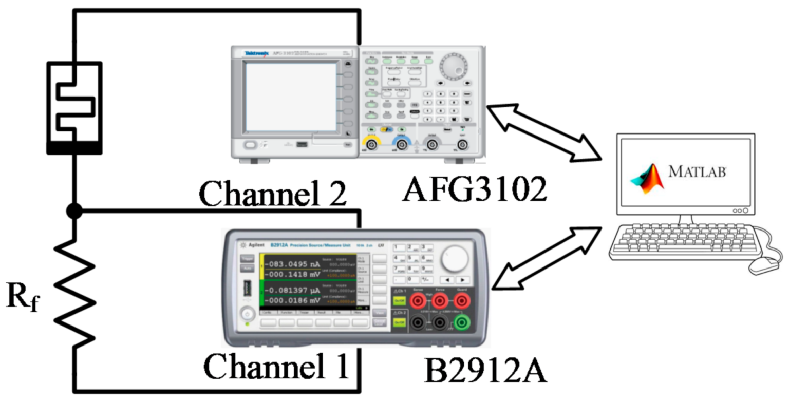
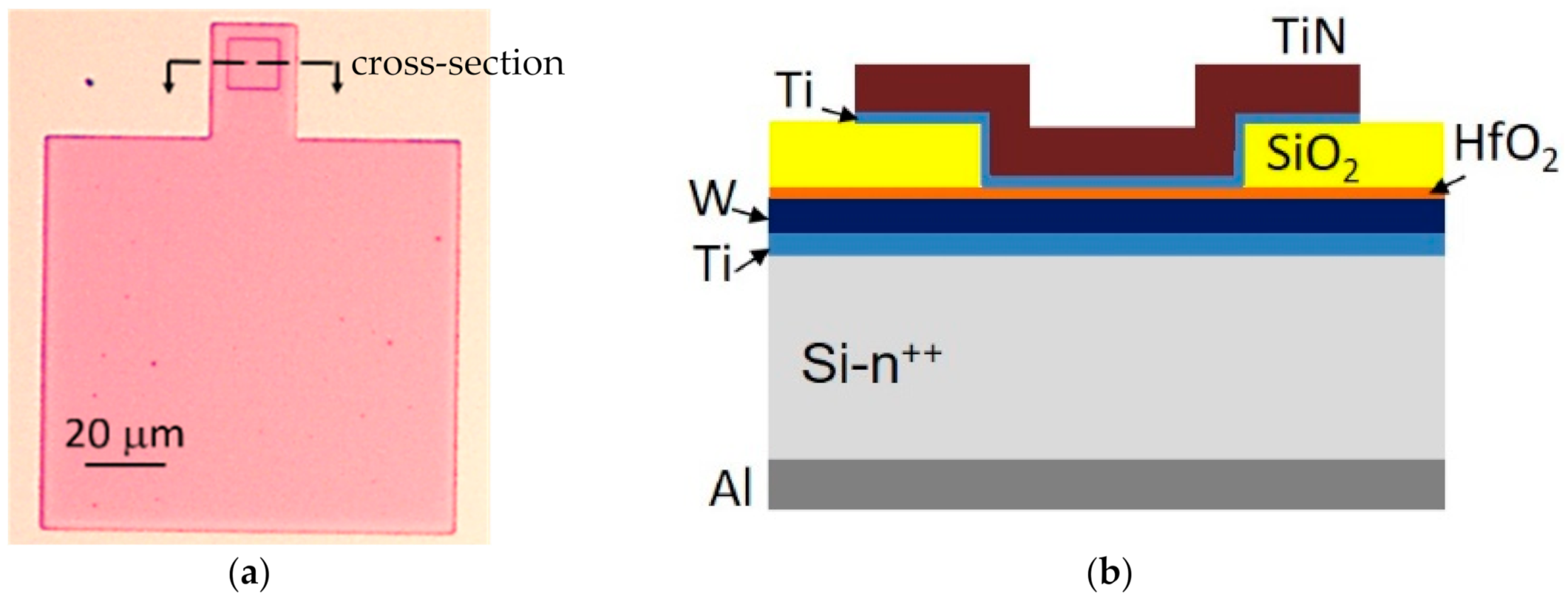
2. Experimental Set-Up

The RRAM devices used in the experiments are TiN/Ti/HfO2/W structures. The 10 nm-thick HfO2 layer was grown by atomic layer deposition (ALD) at 225 °C using TDMAH and H2O as precursors, and the top and bottom metal electrodes were deposited by magnetron sputtering. The bottom electrode consists of a 50 nm-W layer deposited on a 20 nm-Ti adhesion layer on a highly doped n-type silicon wafer, and the top electrode is a 200 nm-TiN on a 10 nm-Ti layer acting as oxygen getter material. Electrical contact to the bottom electrode is made through the Al-metallized back of the silicon wafer. The resulting structures are square cells of 15 × 15 μm2, 5 × 5 μm2 and 2 × 2 µm2. The different sizes of the devices do not have any influence on the results since they reported similar behaviors for the purpose of the present work. A top view optical image is shown in Figure 1a and the corresponding schematic cross-section of the active area is given in Figure 1b.
The electrical characterization of the devices was performed using a Keysight B2912A Precision Source/Measure Unit (SMU) and a Tektronix Arbitrary Function Generator (AFG3102). The set-up is illustrated in Figure 2. For the automatic and successive measurements, the instruments were connected to a computer via GPIB and controlled using MATLAB.

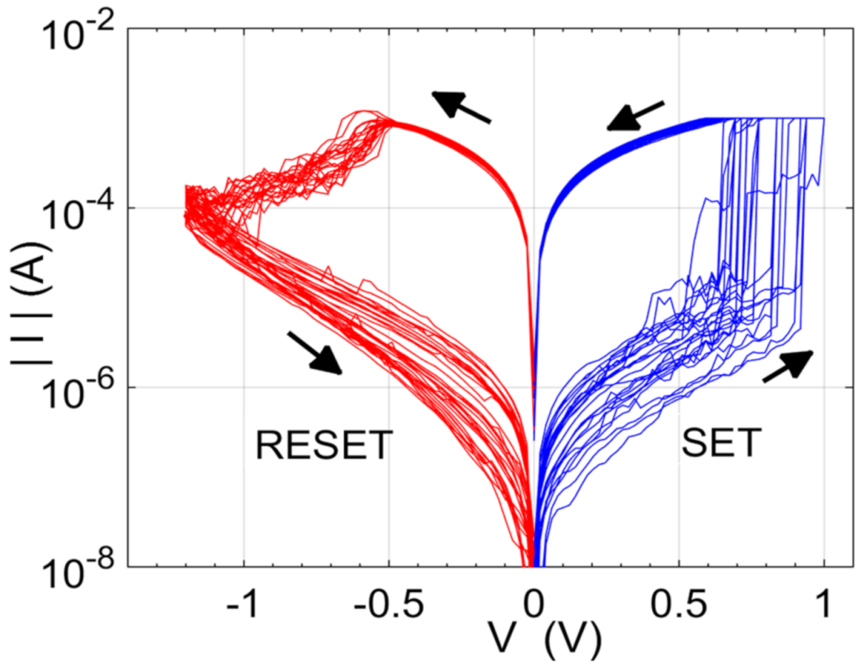
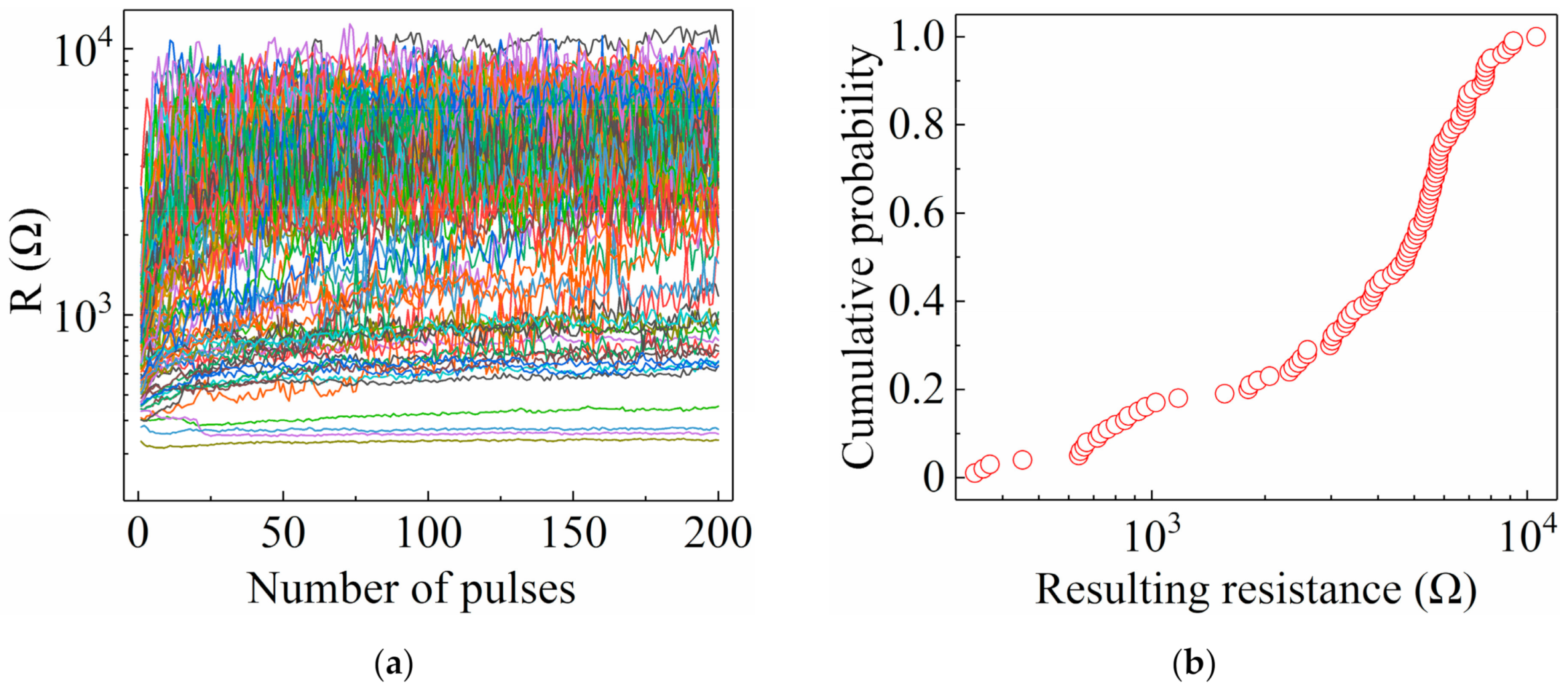
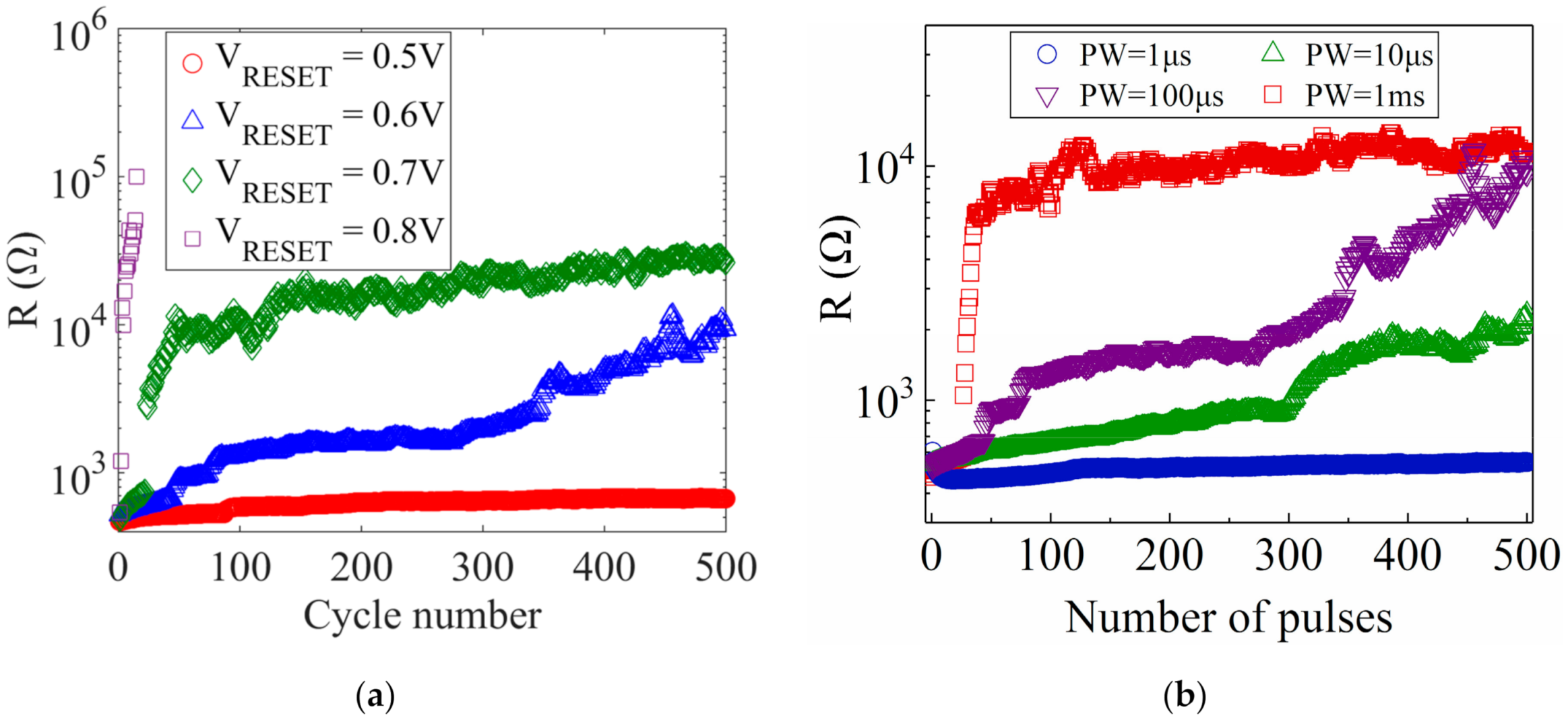
3. Resistance Variability under Pulse Programming

The physical mechanism of RRAMs relies on the formation and dissolution of a conductive filament (CF) composed of defects in oxide (dielectric) between the two metal electrodes. Once this CF is formed, RRAMs can reversibly switch between a high- and a low-resistance state (LRS). This switching behavior is obtained applying a voltage difference across the electrodes. The formation and dissolution of the CF is a stochastic process, generating variability from cell to cell (inter-device variability) and also from cycle-to-cycle (intra-device variability) [23,24]. These statistical fluctuations have a significant impact on the resistance of the device. In this work, we exploit this intra-device variability. In fact, in this section, the variability in the number of pulses applied to the RRAM to reach a specific resistance is analyzed during the RESET operation. The equivalent analysis is not presented for a train of SET pulses due to the abrupt SET characteristic of the target devices. This fact is observed in the DC resistive switching behavior, see Figure 3, where double-sweep voltage ramps were applied from 0 V to +1.1 V for the SET, and from 0 V to −1.4 V for the RESET operations.
After setting the device in the LRS, a train of 500 RESET pulses was subsequently applied. As the goal of the application of this train of pulses is the modulation of the resistive state of the device, the amplitudes of the pulses were significantly lower than those corresponding to a DC RESET operation. The top electrode was grounded and positive pulses (VRESET) were applied to the bottom electrode. The equivalent resistance of the device was obtained measuring the current after every RESET pulse at a read voltage of 0.1 V, a value low enough not to impact the resistance state of the device. Figure 4a shows the evolution of device resistance at different pulse amplitude values while keeping the pulse width constant at 100 μs. It is observed that the higher the pulse amplitude, the lower the number of pulses needed to reach a certain resistance value. Furthermore, intermediate resistance states were reached as pulses were applied. A few pulses were only required to induce a HRS when VRESET = 0.8V. In fact, in this particular case, the train of pulses was stopped when the equivalent resistance of the device was higher than 100 kΩ. Similar behavior was obtained when exponentially varying the pulse width while keeping the RESET pulse amplitude (VRESET) constant (0.6 V), as shown in Figure 4b. Notice that wider pulses lowered the number of pulses needed to reach a specific resistance value. These results are in agreement with previous works [25,26]. However, variability in the intermediate resistance values was observed when trains of RESET pulses were applied to a device departing from the LRS. In Figure 5a, a train of 200 RESET pulses was applied 100 times to the same device. The resistance values show variability after applying each train of pulses. This fact is clearly shown in Figure 5b, where the cumulative probability plot for the resistance of the device is extracted from the results in Figure 5a at the end of every round, i.e., once the train of 200 RESET pulses was applied. The results of Figure 4a and Figure 5a were obtained from two different RRAMs, where a slight device-to-device variability can take place.
Another experiment was conducted to observe the variability in the number of pulses required to drive the device to a threshold resistance of 5000 Ω. The experiment was repeated 43,000 times and the results are shown in Figure 6a. The results show that the number of pulses to reach the threshold resistance is random, although the distribution is not uniform. This fact is observed in the cumulative probability distribution of the number of pulses to drive the device to the threshold resistance, see Figure 6b. Anyway, the variability in the number of pulses is worthy to be taken as a source of randomness.

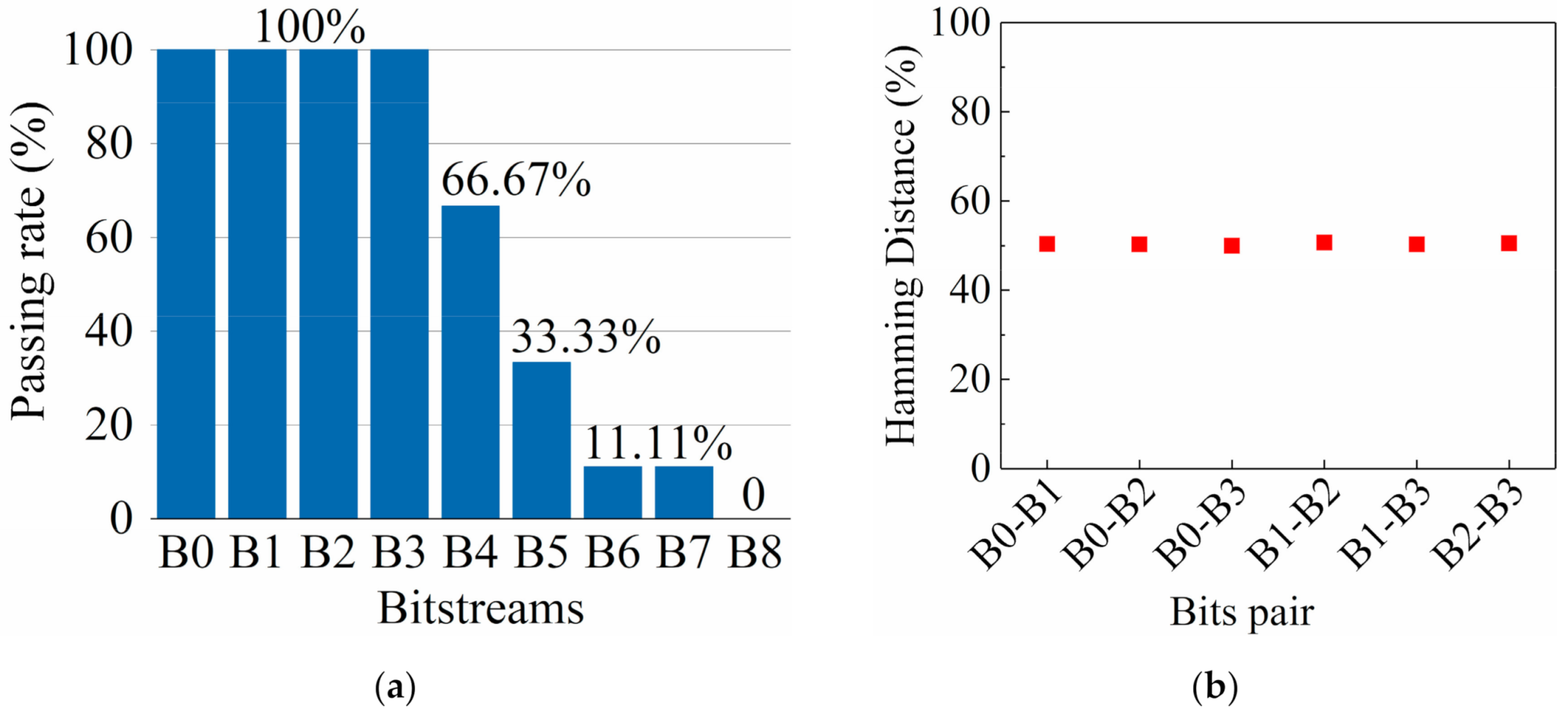
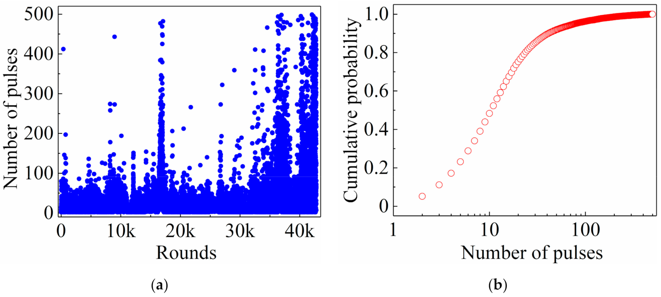
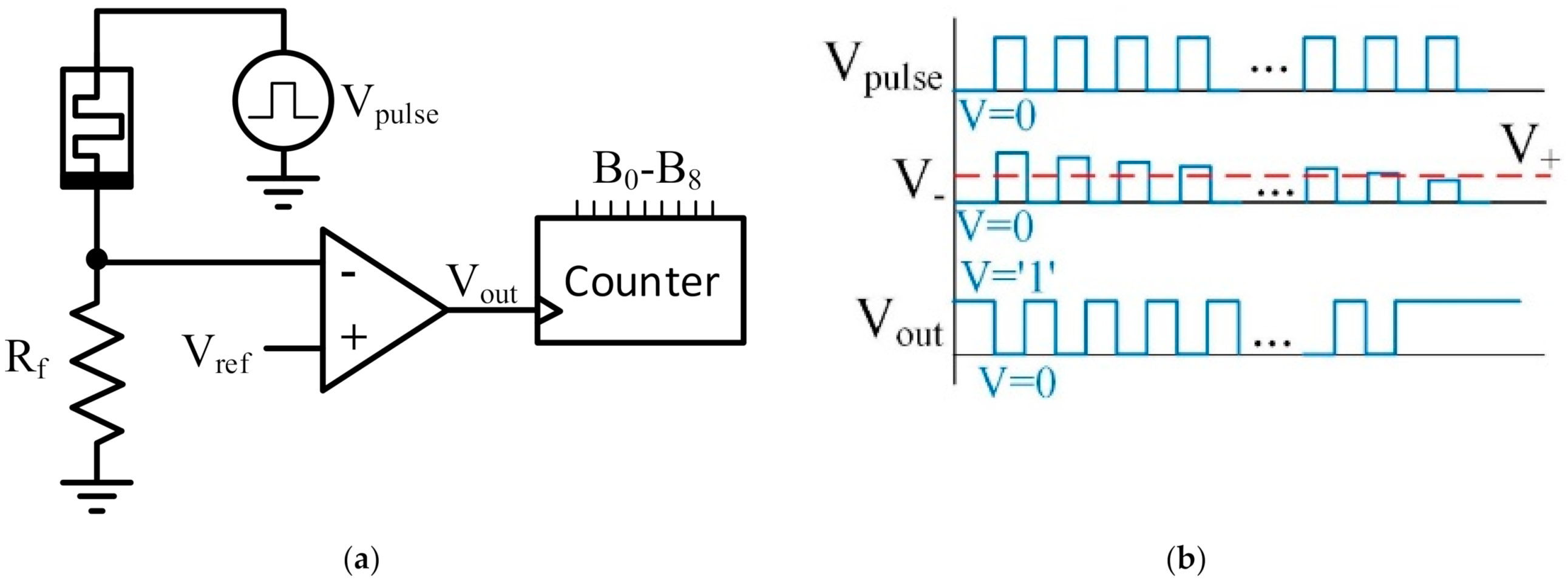
4. Random Number Generator Proposal

The proposed TRNG extracts random bits from the number of RESET pulses required to drive an RRAM to a specific threshold resistance. Figure 7a shows the schematic of the RRAM-based TRNG, which consists of a voltage divider, the RRAM in series with a resistor (Rf = 500 Ω), and a comparator working with Vref. Initially, the device is in the LRS and the counter is set to 0. When the positive voltage pulse (Vpulse) is applied to the bottom terminal of the RRAM (RESET pulse), the voltage divider scales down Vpulse to the voltage at the top electrode terminal (input V- of the comparator), see Figure 7b. As the train of RESET pulses proceeds, the RRAM resistance increases, thus decreasing V-. This voltage is compared to Vref, which is selected according to the threshold resistance and Rf, so that it is used to evaluate whether the device has reached the selected threshold resistance value. When the device resistance is low enough, V- becomes larger than Vref and the comparator produces trains of “0/1”, which are counted by the edge-triggered counter. Once the RRAM resistance reaches the threshold value, V- becomes lower than Vref, and the counter does not count any more pulses. The number of pulses saved in the counter is variable and unpredictable.
An equivalent experiment was conducted and repeated about 20,000 times. According to the observed maximum number of pulses required by the target device to reach the threshold resistance, a 9-bit counter was considered, corresponding then to a maximum of 29 − 1 = 511 RESET pulses to be applied. Therefore, nine bitstreams (B0–B8) coming from the outputs of the counter were recorded synchronously, each of them including near 20,000 values. The applied pulses (Vpulse) were 1.4 V in amplitude and 100 μs in width and the threshold resistance value was 2000 Ω. Notice that the voltage drop across the RRAM is lower than 1.4 V due to the serial resistor (Rf). A nominal RESET and SET pulse were applied between every train of pulses to initialize the device again into the LRS. Although a low throughput was achieved, due to the limitations of the experimental set-up, it would be readily improved by means of a circuit able to apply shorter pulses.
To assess the performance of the proposal, the National Institute of Standards and Technology randomness tests (NIST SP800-22) were used to evaluate the stochasticity of the bitstreams [27]. For each test, a probability value (P-value) was returned and compared to the significance level to check whether the bitstream was random. A specific test was passed only when the resulting P-value was larger than the significance level (0.01), otherwise it failed. According to the length of the bitstreams, a total of 9 out of the 15 tests were performed in all the raw bitstreams without any post-processing. The 6 remaining tests could not be performed due to the length of the bitstreams. The four least significant bits passed all the applied tests and the remaining ones only passed some of them, as indicated in Figure 8a. The detailed results of the B0-B3 bits, which passed all the tests, are shown in Table 1. The accomplished 9 tests proved the quality and non-replicability of the proposed TRNG. Moreover, the inter-Hamming distances among the lowest bitstreams (B0–B3) were evaluated, see Figure 8b. They are close to the ideal 50% value, indicating their high independence level. A further comparison with existing RRAM-based TRNGs can be found in Table 2. The column referred as “NIST passed” reports the number of passed tests related to the number of applied tests. In some cases, it was not possible to apply all the NIST tests (15). According to the results, the presented proposal is competitive, since it is able to generate multiple random bits based on a simple circuit with no need for post-processing. The proposed TRNG passed all the applied NIST tests, although some of them could not be applied due to the length of the bitstream, in a similar way as in other works reported in Table 2.

5. Conclusions

It has been experimentally demonstrated that an RRAM can be exploited as a source for the generation of random numbers by applying trains of RESET pulses. The resistive switching behavior of the RRAM was characterized by varying the amplitude and width of the pulses. Variability was found in the number of RESET pulses required to drive the RRAM to a certain resistance value. An RRAM-based TRNG was further proposed to obtain random bits simultaneously. Experimental measurements were conducted and four of the bitstreams successfully passed all the tests without need for further post-processing, demonstrating the validity of the proposal.

Author Contributions

Conceptualization, D.A.; methodology, B.Y., D.A., S.M. and R.R.-M.; software, B.Y. and D.A.; validation, B.Y., D.A. and S.M.; formal analysis, B.Y., D.A., Á.G.-P., L.F.; investigation, B.Y., D.A.; resources, R.R.-M., M.B.G. and F.C., writing—original draft preparation, B.Y., D.A. and S.M.; writing—review and editing, R.R.-M., Á.G.-P., M.B.G., F.C. and L.F.; funding acquisition, R.R.-M. and F.C. All authors have read and agreed to the published version of the manuscript.

Funding

This research was supported in part by the Spanish Ministry of Science, Innovation and Universities under Grant PID2019-103869RB-C33/ AEI /10.13039/501100011033, and the FEDER program under Grant TEC2017-84321-C4-1-R.

Conflicts of Interest

The authors declare no conflict of interest.

References

  1. Martin, H.; Peris-Lopez, P.; Tapiador, J.E.; San Millan, E. A New TRNG Based on Coherent Sampling With Self-Timed Rings. IEEE Trans. Ind. Inform. 2016, 12, 91–100. [Google Scholar] [CrossRef] [Green Version]
  2. Van der Leest, V.; Maes, R.; Schrijen, G.-J.; Tuyls, P. Hardware Intrinsic Security to Protect Value in the Mobile Market. In ISSE 2014 Securing Electronic Business Processes, Proceedings of the 2014: Information Security Solutions Europe Conference, Brussels, Belgium, 14–15 October 2014; Reimer, H., Pohlmann, N., Schneider, W., Eds.; Springer Vieweg: Wiesbaden, Germany, 2014; pp. 188–198. [Google Scholar] [CrossRef]
  3. Sunar, B.; Martin, W.J.; Stinson, D.R. A Provably Secure True Random Number Generator with Built-In Tolerance to Active Attacks. IEEE Trans. Comput. 2007, 56, 109–119. [Google Scholar] [CrossRef]
  4. Bucci, M.; Germani, L.; Luzzi, R.; Trifiletti, A.; Varanonuovo, M. A high-speed oscillator-based truly random number source for cryptographic applications on a smart card IC. IEEE Trans. Comput. 2003, 52, 403–409. [Google Scholar] [CrossRef]
  5. Brederlow, R.; Prakash, R.; Paulus, C.; Thewes, R. A low-power true random number generator using random telegraph noise of single oxide-traps. In Proceedings of the 2006 IEEE International Solid State Circuits Conference—Digest of Technical, San Francisco, CA, USA, 6–9 February 2006; pp. 1666–1675. [Google Scholar] [CrossRef]
  6. Yasuda, S.; Satake, H.; Tanamoto, T.; Ohba, R.; Uchida, K.; Fujita, S. Physical random number generator based on MOS structure after soft breakdown. IEEE J. Solid-State Circuits. 2004, 39, 1375–1377. [Google Scholar] [CrossRef]
  7. Wu, H.; Wang, X.H.; Gao, B.; Deng, N.; Lu, Z.; Haukness, B.; Bronner, G.; Qian, H. Resistive random access memory for future information processing system. Proc. IEEE 2017, 105, 1770–1789. [Google Scholar] [CrossRef]
  8. Ielmini, D. Brain-inspired computing with resistive switching memory (RRAM): Devices, synapses and neural networks. Microelectron. Eng. 2018, 190, 44–53. [Google Scholar] [CrossRef]
  9. Kvatinsky, S.; Satat, G.; Wald, N.; Friedman, E.G.; Kolodny, A.; Weiser, U.C. Memristor-Based Material Implication (IMPLY) Logic: Design Principles and Methodologies. IEEE Trans. Very Large Scale Integr. (VLSI) Syst. 2014, 22, 2054–2066. [Google Scholar] [CrossRef]
  10. González-Cordero, G.; González, M.B.; Campabadal, F.; Jiménez-Molinos, F.; Roldán, J.B. A new technique to analyze RTN signals in resistive memories. Microelectron. Eng. 2019, 215, 110994. [Google Scholar] [CrossRef]
  11. Simanjuntak, F.M.; Chandrasekaran, S.; Lin, C.-C.; Tseng, T.-Y. Switching Failure Mechanism in Zinc Peroxide-Based Programmable Metallization Cell. Nanoscale. Res. Lett. 2018, 13, 327. [Google Scholar] [CrossRef]
  12. Huang, X.D.; Li, Y.; Li, H.Y.; Lu, Y.F.; Xue, K.H.; Miao, X.S. Enhancement of DC/AC resistive switching performance in AlOx memristor by two-technique bilayer approach. Appl. Phys. Lett. 2020, 116, 173504. [Google Scholar] [CrossRef]
  13. Rajendran, J.; Karri, R.; Wendt, J.B.; Potkonjak, M.; McDonald, N.; Rose, G.S.; Wysocki, B. Nano meets security: Exploring nanoelectronic devices for security applications. Proc. IEEE 2015, 103, 829–849. [Google Scholar] [CrossRef]
  14. Jiang, H.; Belkin, D.; Savel’ev, S.E.; Lin, S.; Wang, Z.; Li, Y.; Joshi, S.; Midya, R.; Li, C.; Rao, M.; et al. A novel true random number generator based on a stochastic diffusive memristor. Nat. Commun. 2017, 8, 882. [Google Scholar] [CrossRef] [Green Version]
  15. Postel-Pellerin, J.; Bazzi, H.; Aziza, H.; Canet, P.; Moreau, M.; Della Marca, V.; Harb, A. True random number generation exploiting SET voltage variability in resistive RAM memory arrays. In Proceedings of the 2019 19th Non-Volatile Memory Technology Symposium (NVMTS), Durham, NC, USA, 28–30 October 2019; pp. 1–5. [Google Scholar] [CrossRef]
  16. Cambou, B.; Telesca, D.; Assiri, S.; Garrett, M.; Jain, S.; Partridge, M. TRNGs from Pre-Formed ReRAM Arrays. Cryptography 2021, 5, 8. [Google Scholar] [CrossRef]
  17. Balatti, S.; Ambrogio, S.; Carboni, R.; Milo, V.; Wang, Z.; Calderoni, A.; Ramaswamy, N.; Ielmini, D. Physical Unbiased Generation of Random Numbers With Coupled Resistive Switching Devices. IEEE Trans. Electron Devices 2016, 63, 2029–2035. [Google Scholar] [CrossRef] [Green Version]
  18. Zhang, T.; Yin, M.; Xu, C.; Lu, X.; Sun, X.; Yang, Y.; Huang, R. High-speed true random number generation based on paired memristors for security electronics. Nanotechnology 2017, 28, 455202. [Google Scholar] [CrossRef]
  19. Aziza, H.; Postel-Pellerin, J.; Bazzi, H.; Canet, P.; Moreau, M.; Della Marca, V.; Harb, A. True Random Number Generator Integration in a Resistive RAM Memory Array Using Input Current Limitation. IEEE Trans. Nanotechnol. 2020, 19, 214–222. [Google Scholar] [CrossRef]
  20. Huang, C.-Y.; Shen, W.C.; Tseng, Y.-H.; King, Y.-C.; Lin, C.-J. A Contact-Resistive Random-Access-Memory-Based True Random Number Generator. IEEE Electron Device Lett. 2012, 33, 1108–1110. [Google Scholar] [CrossRef]
  21. Govindaraj, R.; Ghosh, S.; Katkoori, S. CSRO-Based Reconfigurable True Random Number Generator Using RRAM. IEEE Trans. Very Large Scale Integr. (VLSI) Syst. 2018, 26, 2661–2670. [Google Scholar] [CrossRef]
  22. Kim, J.; Nili, H.; Truong, N.D.; Ahmed, T.; Yang, J.; Jeong, D.S.; Sriram, S.; Ranasinghe, D.C.; Ippolito, S.; Chun, H.; et al. Nano-Intrinsic True Random Number Generation: A Device to Data Study. IEEE Trans. Circuits Syst. I Reg. Pap. 2019, 66, 2615–2626. [Google Scholar] [CrossRef]
  23. Larentis, S.; Nardi, F.; Balatti, S.; Gilmer, D.C.; Ielmini, D. Resistive switching by voltage-driven ion migration in bipolar RRAM—Part II: Modeling. IEEE Trans. Electron Devices 2012, 59, 2468–2475. [Google Scholar] [CrossRef]
  24. Miranda, E. Compact model for the major and minor hysteretic I-V loops in nonlinear memristive devices. IEEE Trans. Nanotechnol. 2015, 14, 787–789. [Google Scholar] [CrossRef]
  25. Poblador, S.; Gonzalez, M.B.; Campabadal, F. Investigation of the multilevel capability of TiN/Ti/HfO2/W resistive switching devices by sweep and pulse programming. Microelectron. Eng. 2018, 187–188, 148–153. [Google Scholar] [CrossRef]
  26. García, H.; Ossorio, O.G.; Dueñas, S.; Castán, H. Controlling the intermediate conductance states in RRAM devices for synaptic applications. Microelectron. Eng. 2019, 215, 110984. [Google Scholar] [CrossRef]
  27. Bassham III, L.E.; Rukhin, A.L.; Soto, J.; Nechvatal, J.R.; Smid, M.E.; Barker, E.B.; Leigh, S.D.; Levenson, M.; Vangel, M.; Banks, D.L.; et al. A Statistical Test Suite for Random and Pseudorandom Number Generators for Cryptographic Applications; Technical Report for National Institute of Standards and Technology: Gaithersburg, MD, USA, 2010. [CrossRef]
Figure 1. (a) Top-view optical microscope image. (b) Schematic device cross-section pinpointed in (a).
Electronics 10 01831 g001
Figure 2. Experimental set-up.
Electronics 10 01831 g002
Figure 3. DC resistive switching behavior during successive SET and RESET operations.
Electronics 10 01831 g003
Figure 4. (a) Device resistance applying RESET pulses departing from LRS for different pulse amplitudes (VRESET) with constant pulse width (100 μs). (b) Device resistance applying RESET pulses departing from LRS for different pulse widths (PW) with VRESET = 0.6 V.
Electronics 10 01831 g004
Figure 5. (a) Variability of device resistance for 100 trains of 200 RESET pulses. The applied pulses were 0.9 V in amplitude and 100 μs in width. The device was in the LRS before the application of each train of pulses. (b) Cumulative probability distribution of device resistance after 200 RESET pulses.
Electronics 10 01831 g005
Figure 6. (a) Number of RESET pulses (VRESET = 0.9 V) to reach a threshold resistance (5000 Ω). (b) Cumulative probability distribution of the number of pulses.
Electronics 10 01831 g006
Figure 7. (a) Schematic of the proposed TRNG (resistive divider, Vref, comparator, and a counter). (b) Diagram of the voltage pulse operation.
Electronics 10 01831 g007
Figure 8. (a) NIST tests passing rate for the nine generated bitstreams. (b) Hamming distances among the bitstreams passing the NIST tests (B0–B3).
Electronics 10 01831 g008
Table 1. NIST SP800-22 test results for bits B0-B3. A specific test was passed when the P-value was larger than the significance level (0.01).
TestB0B1B2B3
P-valueP-valueP-valueP-value
Frequency0.823400.879830.058310.57935
Block frequency0.036990.633010.098920.23719
Runs0.458170.789830.101530.69051
Longest run of ones0.460350.762490.965690.72316
Spectral DFT0.167870.591430.395010.06316
Non-overlapping template a0.530670.472080.471760.50414
Serial 10.066430.470750.037910.67948
Serial 20.118290.717130.292770.80299
Approximate entropy0.083840.286950.187050.23089
Cumulative sum (forward)0.941120.589620.016830.60898
Cumulative sum (reverse)0.762930.729260.051270.23647
a An average P-value is adopted for the Non-Overlapping template test.
Table 2. Comparative analysis of RRAM-based TRNGs.
WorkEntropy Source# of RRAMs RRAM IntegrationExtra Circuitry# of Random BitsNIST Passed Post-Processing
[14]Switching delay1Single cellComparator, AND and counter615/15No
[15]Probabilistic switching11T-1R
(7 × 7 array)
Comparator111/15No
[16]Inter-device variability22 Mbit arrayComparator110/10XOR
[17]Switching delay2Single cellComparator19/15Von Neumann
[18]Inter- and intra-device switching variability.21 × 2 arrayComparator112/15Von Neumann
[19]RRAM switching current17 × 7 arrayComparator112/15XOR
[20]RTN1Single cellComparator and D Flip-flop15/15No
[21]RTN and intra-device switching variability11T-1R
(Simulation)
Ring oscillator and D Flip-flop.112/12No
[22]RTN2Single cellComparator and DAC115/15Von Neumann
This workIntra-device RESET switching variability1Single cellComparator and counter49/9No
Publisher’s Note: MDPI stays neutral with regard to jurisdictional claims in published maps and institutional affiliations.

