
Effects of Chamber Pressures on the Passivation Layer of Hydrogenated Nano-Crystalline Silicon Mixed-Phase Thin Film by Using Microwave Annealing


Abstract
1. Introduction
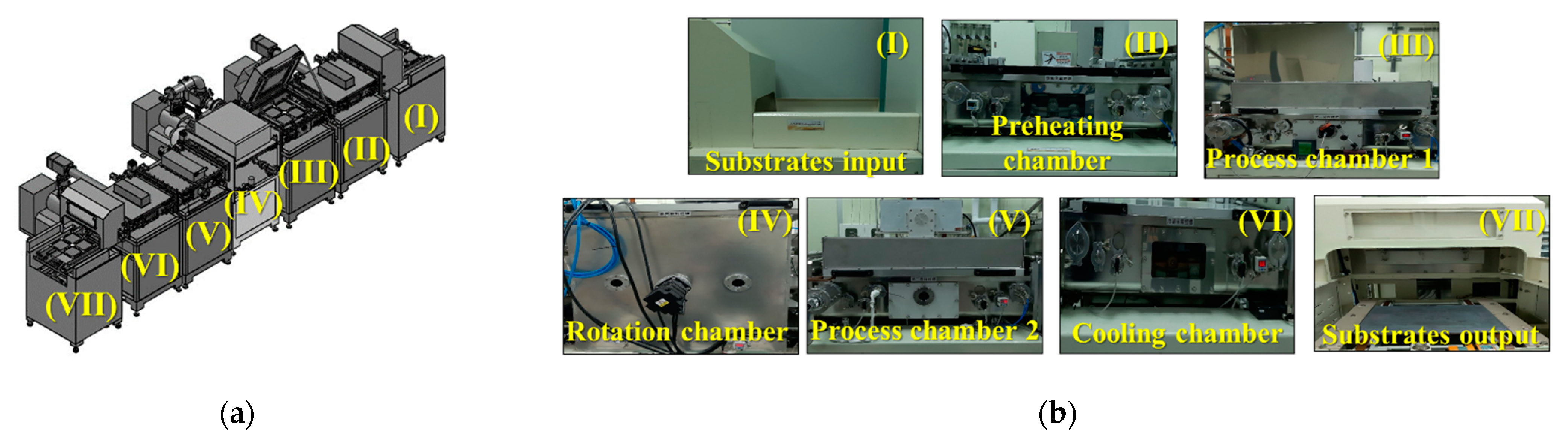
2. Materials and Methods
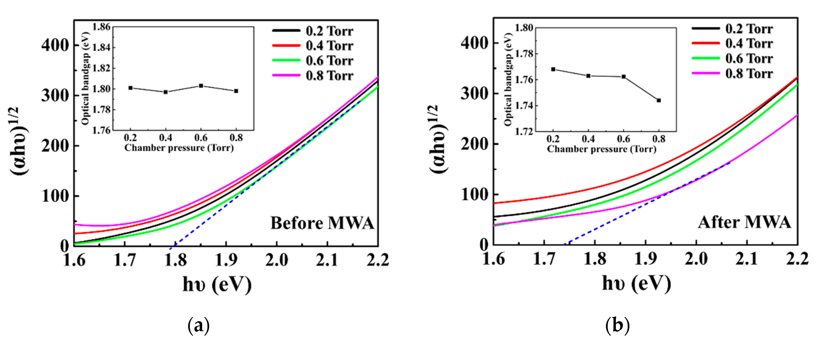
3. Results and Discussion
4. Conclusions
Author Contributions
Funding
Data Availability Statement
Acknowledgments
Conflicts of Interest
References
- Rahman, M.Z.; Khan, S.I. Advances in Surface Passivation of C-Si Solar Cells. Mater. Renew. Sustain. Energy. 2012, 1, 1. [Google Scholar] [CrossRef]
- Aberle, A.G. Surface Passivation of Crystalline Silicon Solar Cells: A Review. Prog. Photovolt. Res. Appl. 2000, 8, 473–487. [Google Scholar] [CrossRef]
- Anna Selvan, J.A.; Delahoy, A.E.; Guo, S.; Li, Y.-M. A New Light Trapping TCO for Nc-Si:H Solar Cells. Sol. Energy Mater. Sol. Cells. 2006, 90, 3371–3376. [Google Scholar] [CrossRef]
- Shim, J.-H.; Im, S.; Cho, N.-H. Nanostructural Features of Nc-Si:H Thin Films Prepared by PECVD. Appl. Surf. Sci. 2004, 234, 268–273. [Google Scholar] [CrossRef]
- Wen, C.; Xu, H.; Liu, H.; Li, Z.; Shen, W. Passivation of Nanocrystalline Silicon Photovoltaic Materials Employing a Negative Substrate Bias. Nanotechnology 2013, 24, 455602. [Google Scholar] [CrossRef] [PubMed]
- Zhang, Q.; Zhu, M.; Liu, F.; Zhou, Y. The Optimization of Interfacial Properties of Nc-Si:H/c-Si Solar Cells in Hot-Wire Chemical Vapor Deposition Process. J. Mater. Sci. Mater. Electron. 2007, 18, 33–36. [Google Scholar] [CrossRef]
- Sharma, M.; Panigrahi, J.; Komarala, V.K. Nanocrystalline Silicon Thin Film Growth and Application for Silicon Heterojunction Solar Cells: A Short Review. Nanoscale Adv. 2021, 3, 3373–3383. [Google Scholar] [CrossRef]
- Zhang, R.; Chen, X.Y.; Zhang, K.; Shen, W.Z. Photocurrent Response of Hydrogenated Nanocrystalline Silicon Thin Films. J. Appl. Phys. 2006, 100, 104310. [Google Scholar] [CrossRef]
- Chen, X.Y.; Shen, W.Z.; He, Y.L. Enhancement of Electron Mobility in Nanocrystalline Silicon∕crystalline Silicon Heterostructures. J. Appl. Phys. 2005, 97, 024305. [Google Scholar] [CrossRef]
- Keppner, H.; Meier, J.; Torres, P.; Fischer, D.; Shah, A. Microcrystalline Silicon and Micromorph Tandem Solar Cells. Appl. Phys. 1999, A 69, 169–177. [Google Scholar] [CrossRef]
- Edelberg, E.; Bergh, S.; Naone, R.; Hall, M.; Aydil, E.S. Visible Luminescence from Nanocrystalline Silicon Films Produced by Plasma Enhanced Chemical Vapor Deposition. Appl. Phys. Lett. 1996, 68, 1415–1417. [Google Scholar] [CrossRef]
- Zaknoon, B.; Bahir, G.; Saguy, C.; Edrei, R.; Hoffman, A.; Rao, R.A.; Muralidhar, R.; Chang, K.-M. Study of Single Silicon Quantum Dots’ Band Gap and Single-Electron Charging Energies by Room Temperature Scanning Tunneling Microscopy. Nano Lett. 2008, 8, 1689–1694. [Google Scholar] [CrossRef] [PubMed]
- Gonçalves, C.; Charvet, S.; Zeinert, A.; Clin, M.; Zellama, K. Nanocrystalline Silicon Thin Films Prepared by Radiofrequency Magnetron Sputtering. Thin Solid Films 2002, 403–404, 91–96. [Google Scholar] [CrossRef]
- Fonrodona, M.; Soler, D.; Escarré, J.; Villar, F.; Bertomeu, J.; Andreu, J.; Saboundji, A.; Coulon, N.; Mohammed-Brahim, T. Low Temperature Amorphous and Nanocrystalline Silicon Thin Film Transistors Deposited by Hot-Wire CVD on Glass Substrate. Thin Solid Films 2006, 501, 303–306. [Google Scholar] [CrossRef][Green Version]
- Takatsuka, H.; Noda, M.; Yonekura, Y.; Takeuchi, Y.; Yamauchi, Y. Development of High Efficiency Large Area Silicon Thin Film Modules Using VHF-PECVD. Sol. Energy 2004, 77, 951–960. [Google Scholar] [CrossRef]
- Dutta, J.; Kroll, U.; Chabloz, P.; Shah, A.; Howling, A.A.; Dorier, J.-L.; Hollenstein, C. Dependence of Intrinsic Stress in Hydrogenated Amorphous Silicon on Excitation Frequency in a Plasma-enhanced Chemical Vapor Deposition Process. J. Appl. Phys. 1992, 72, 3220–3222. [Google Scholar] [CrossRef]
- Surendra, M.; Graves, D.B. Capacitively Coupled Glow Discharges at Frequencies above 13.56 MHz. Appl. Phys. Lett. 1991, 59, 2091–2093. [Google Scholar] [CrossRef]
- Kitajima, T.; Takeo, Y.; Nakano, N.; Makabe, T. Effects of Frequency on the Two-Dimensional Structure of Capacitively Coupled Plasma in Ar. J. Appl. Phys. 1998, 84, 5928–5936. [Google Scholar] [CrossRef]
- Takagi, T.; Takechi, K.; Nakagawa, Y.; Watabe, Y.; Nishida, S. High Rate Deposition of A-Si:H and a-SiNx:H by VHF PECVD. Vacuum 1998, 51, 751–755. [Google Scholar] [CrossRef]
- Curtins, H.; Wyrsch, N.; Favre, M.; Shah, A.V. Influence of Plasma Excitation Frequency Fora-Si:H Thin Film Deposition. Plasma Chem. Plasma Process. 1987, 7, 267–273. [Google Scholar] [CrossRef]
- Batey, J.; Tierney, E. Low-temperature Deposition of High-quality Silicon Dioxide by Plasma-enhanced Chemical Vapor Deposition. J. Appl. Phys. 1986, 60, 3136–3145. [Google Scholar] [CrossRef]
- Matsui, T.; Kondo, M.; Matsuda, A. Origin of the Improved Performance of High-Deposition-Rate Microcrystalline Silicon Solar Cells by High-Pressure Glow Discharge. Jpn. J. Appl. Phys. 2003, 42, L901. [Google Scholar] [CrossRef]
- Gordijn, A.; Vanecek, M.; Goedheer, W.J.; Rath, J.K.; Schropp, R.E.I. Influence of Pressure and Plasma Potential on High Growth Rate Microcrystalline Silicon Grown by Very High Frequency Plasma Enhanced Chemical Vapour Deposition. Jpn. J. Appl. Phys. 2006, 45, 6166. [Google Scholar] [CrossRef]
- Sobajima, Y.; Nishino, M.; Fukumori, T.; Kurihara, M.; Higuchi, T.; Nakano, S.; Toyama, T.; Okamoto, H. Solar Cell of 6.3% Efficiency Employing High Deposition Rate (8 nm/s) Microcrystalline Silicon Photovoltaic Layer. Sol. Energy Mater. Sol. Cells 2009, 93, 980–983. [Google Scholar] [CrossRef]
- Klein, S.; Repmann, T.; Brammer, T. Microcrystalline Silicon Films and Solar Cells Deposited by PECVD and HWCVD. Sol. Energy 2004, 77, 893–908. [Google Scholar] [CrossRef]
- Yang, H.J.; Ji, K.; Choi, J.; Lee, H.M. Annealing Effect on Surface Passivation of A-Si:H/c-Si Interface in Terms of Crystalline Volume Fraction. Curr. Appl. Phys. 2010, 10, S375–S378. [Google Scholar] [CrossRef]
- Ai, Y.; Yuan, H.-C.; Page, M.; Nemeth, W.; Roybal, L.; Gedvilas, L.; Wang, Q. Process Optimization for High Efficiency Heterojunction C-Si Solar Cells Fabrication Using Hot-Wire Chemical Vapor Deposition. In Proceedings of the 2012 38th IEEE Photovoltaic Specialists Conference, Austin, TX, USA, 3–8 June 2012; pp. 988–991. [Google Scholar]
- De Wolf, S.; Demaurex, B.; Descoeudres, A.; Ballif, C. Very Fast Light-Induced Degradation of $a$-Si:H/$c$-Si(100) Interfaces. Phys. Rev. B 2011, 83, 233301. [Google Scholar] [CrossRef]
- Luo, Y.; Sui, X.; He, Y.; Huang, H.; Zhou, N.; Zhou, L. The Influence of Annealing Temperature upon the Structure of A-Si:H/c-Si Thin Films. J. Non-Cryst. Solids 2017, 471, 379–383. [Google Scholar] [CrossRef]
- Stöhr, M.; Aprojanz, J.; Brendel, R.; Dullweber, T. Firing-Stable PECVD SiOxNy/n-Poly-Si Surface Passivation for Silicon Solar Cells. ACS Appl. Energy Mater. 2021, 4, 4646–4653. [Google Scholar] [CrossRef]
- Schulze, T.F.; Beushausen, H.N.; Hansmann, T.; Korte, L.; Rech, B. Accelerated Interface Defect Removal in Amorphous/Crystalline Silicon Heterostructures Using Pulsed Annealing and Microwave Heating. Appl. Phys. Lett. 2009, 95, 182108. [Google Scholar] [CrossRef]
- Lu, Y.-L.; Lee, Y.-J.; Chao, T.-S. Simultaneous Activation and Crystallization by Low-Temperature Microwave Annealing for Improved Quality of Amorphous Silicon Thin-Film Transistors. ECS Solid State Lett. 2012, 1, P1. [Google Scholar] [CrossRef]
- Lee, Y.-J.; Cho, T.-C.; Chuang, S.-S.; Hsueh, F.-K.; Lu, Y.-L.; Sung, P.-J.; Chen, H.-C.; Current, M.I.; Tseng, T.-Y.; Chao, T.-S.; et al. Low-Temperature Microwave Annealing Processes for Future IC Fabrication—A Review. IEEE Trans. Electron Devices 2014, 61, 651–665. [Google Scholar] [CrossRef]
- Hu, H.-H.; Huang, H.-P. High-Frequency Performance of Trigate Poly-Si Thin-Film Transistors by Microwave Annealing. IEEE Electron Device Lett. 2015, 36, 345–347. [Google Scholar] [CrossRef]
- Shih, T.-L.; Su, Y.-H.; Kuo, T.-C.; Lee, W.-H.; Current, M.I. Effect of Microwave Annealing on Electrical Characteristics of TiN/Al/TiN/HfO2/Si MOS Capacitors. Appl. Phys. Lett. 2017, 111, 012101. [Google Scholar] [CrossRef]
- Fu, C.; Wang, Y.; Xu, P.; Yue, L.; Sun, F.; Zhang, D.W.; Zhang, S.-L.; Luo, J.; Zhao, C.; Wu, D. Understanding the Microwave Annealing of Silicon. AIP Adv. 2017, 7, 035214. [Google Scholar] [CrossRef]
- Lihui, G.; Rongming, L. Studies on the Formation of Microcrystalline Silicon with PECVD under Low and High Working Pressure. Thin Solid Films 2000, 376, 249–254. [Google Scholar] [CrossRef]
- Wang, Y.; Liu, H.; Shen, W. A Convenient and Effective Method to Deposit Low-Defect-Density Nc-Si:H Thin Film by PECVD. Nanoscale Res. Lett. 2018, 13, 234. [Google Scholar] [CrossRef]
- Suzuki, S.; Kondo, M.; Matsuda, A. Growth of Device Grade Μc-Si Film at over 50Å/s Using PECVD. Sol. Energy Mater. Sol. Cells 2002, 74, 489–495. [Google Scholar] [CrossRef]
- Wei, C.-Y.; Lin, C.-H.; Hsiao, H.-T.; Yang, P.-C.; Wang, C.-M.; Pan, Y.-C. Efficiency Improvement of HIT Solar Cells on P-Type Si Wafers. Materials 2013, 6, 5440–5446. [Google Scholar] [CrossRef]
- Liang, X.; Sperling, B.A.; Calizo, I.; Cheng, G.; Hacker, C.A.; Zhang, Q.; Obeng, Y.; Yan, K.; Peng, H.; Li, Q.; et al. Toward Clean and Crackless Transfer of Graphene. ACS Nano 2011, 5, 9144–9153. [Google Scholar] [CrossRef]
- De Wolf, S.; Olibet, S.; Ballif, C. Stretched-Exponential a-Si:H/c-Si Interface Recombination Decay. Appl. Phys. Lett. 2008, 93, 032101. [Google Scholar] [CrossRef]
- Andújar, J.L.; Bertran, E.; Canillas, A.; Roch, C.; Morenza, J.L. Influence of Pressure and Radio Frequency Power on Deposition Rate and Structural Properties of Hydrogenated Amorphous Silicon Thin Films Prepared by Plasma Deposition. J. Vac. Sci. Technol. A 1991, 9, 2216–2221. [Google Scholar] [CrossRef]
- Matsuda, A. Growth Mechanism of Microcrystalline Silicon Obtained from Reactive Plasmas. Thin Solid Films 1999, 337, 1–6. [Google Scholar] [CrossRef]
- Bustarret, E.; Hachicha, M.A.; Brunel, M. Experimental Determination of the Nanocrystalline Volume Fraction in Silicon Thin Films from Raman Spectroscopy. Appl. Phys. Lett. 1988, 52, 1675–1677. [Google Scholar] [CrossRef]
- Droz, C.; Vallat-Sauvain, E.; Bailat, J.; Feitknecht, L.; Meier, J.; Shah, A. Relationship between Raman Crystallinity and Open-Circuit Voltage in Microcrystalline Silicon Solar Cells. Sol. Energy Mater. Sol. Cells 2004, 81, 61–71. [Google Scholar] [CrossRef]
- Tsu, R.; Gonzalez-Hernandez, J.; Chao, S.S.; Lee, S.C.; Tanaka, K. Critical Volume Fraction of Crystallinity for Conductivity Percolation in Phosphorus-doped Si:F:H Alloys. Appl. Phys. Lett. 1982, 40, 534–535. [Google Scholar] [CrossRef]
- Amrani, R.; Pichot, F.; Podlecki, J.; Foucaran, A.; Chahed, L.; Cuminal, Y. Optical and Structural Proprieties of Nc-Si:H Prepared by Argon Diluted Silane PECVD. J. Non-Cryst. Solids 2012, 358, 1978–1982. [Google Scholar] [CrossRef]
- Funde, A.M.; Bakr, N.A.; Kamble, D.K.; Hawaldar, R.R.; Amalnerkar, D.P.; Jadkar, S.R. Influence of Hydrogen Dilution on Structural, Electrical and Optical Properties of Hydrogenated Nanocrystalline Silicon (Nc-Si:H) Thin Films Prepared by Plasma Enhanced Chemical Vapour Deposition (PE-CVD). Sol. Energy Mater. Sol. Cells 2008, 92, 1217–1223. [Google Scholar] [CrossRef]
- Kroll, U.; Meier, J.; Shah, A.; Mikhailov, S.; Weber, J. Hydrogen in Amorphous and Microcrystalline Silicon Films Prepared by Hydrogen Dilution. J. Appl. Phys. 1996, 80, 4971–4975. [Google Scholar] [CrossRef]
- Shim, J.-H.; Cho, N.-H. Structural and Chemical Features of Silicon Nanocrystallites in Nanocrystalline Hydrogenated Silicon Thin Films. Glass Phys. Chem. 2005, 31, 525–529. [Google Scholar] [CrossRef]
- Lucovsky, G.; Nemanich, R.J.; Knights, J.C. Structural Interpretation of the Vibrational Spectra of $a$-Si:H Alloys. Phys. Rev. B 1979, 19, 2064–2073. [Google Scholar] [CrossRef]
- Peng, C.H.; Chang, J.-F.; Desu, S.B. Optical Properties of PZT, PLZT, and PNZT Thin Films. MRS Online Proc. Libr. OPL 1991, 243. [Google Scholar] [CrossRef]
- Yang, S.; Mo, D.; Tang, X. Determination of the Optical Properties of Sol-Gel-Derived Pb(Zr x Ti (1 − x ) )O 3 Thin Films by Spectroscopic Ellipsometry. Ferroelectrics 2003, 287, 35–46. [Google Scholar] [CrossRef]
- Li, W.; Xia, D.; Wang, H.; Zhao, X. Hydrogenated Nanocrystalline Silicon Thin Film Prepared by RF-PECVD at High Pressure. J. Non-Cryst. Solids 2010, 356, 2552–2556. [Google Scholar] [CrossRef]
- Jadhavar, A.; Pawbake, A.; Waykar, R.; Jadkar, V.; Kulkarni, R.; Bhorde, A.; Rondiya, S.; Funde, A.; Patil, D.; Date, A.; et al. Growth of Hydrogenated Nano-Crystalline Silicon (Nc-Si:H) Films by Plasma Enhanced Chemical Vapor Deposition (PE-CVD). Energy Procedia 2017, 110, 45–52. [Google Scholar] [CrossRef]
- Wang, Y.H.; Lin, J.; Huan, C.H.A. Structural and Optical Properties of A-Si:H/Nc-Si:H Thin Films Grown from Ar–H2–SiH4 Mixture by Plasma-Enhanced Chemical Vapor Deposition. Mater. Sci. Eng. B 2003, 104, 80–87. [Google Scholar] [CrossRef]
- Canham, L.T. Silicon Quantum Wire Array Fabrication by Electrochemical and Chemical Dissolution of Wafers. Appl. Phys. Lett. 1990, 57, 1046–1048. [Google Scholar] [CrossRef]
- Juneja, S.; Sudhakar, S.; Gope, J.; Kumar, S. Mixed Phase Silicon Thin Films Grown at High Rate Using 60MHz Assisted VHF-PECVD Technique. Mater. Sci. Semicond. Process. 2015, 40, 11–19. [Google Scholar] [CrossRef]
- Schulze, T.F.; Beushausen, H.N.; Leendertz, C.; Dobrich, A.; Rech, B.; Korte, L. Interplay of Amorphous Silicon Disorder and Hydrogen Content with Interface Defects in Amorphous/Crystalline Silicon Heterojunctions. Appl. Phys. Lett. 2010, 96, 252102. [Google Scholar] [CrossRef]
- Guo, C.-L.; Wang, L.; Zhang, Y.-R.; Zhou, H.-F.; Liang, F.; Yang, Z.-H.; Yang, D.-R. High-Pressure Water-Vapor Annealing for Enhancement of a-Si:H Film Passivation of Silicon Surface. Chin. Phys. Lett. 2014, 31, 108501. [Google Scholar] [CrossRef]
- Chu, Y.-H.; Lee, C.-C.; Chang, T.-H.; Hsieh, Y.-L.; Liu, S.-M.; Chang, J.-Y.; Li, T.T.; Chen, I.-C. Investigation of A-Si:H Films as Passivation Layer in Heterojunction Interface at Low Temperature. ECS Trans. 2014, 60, 1245. [Google Scholar] [CrossRef]
- Ruan, T.; Qu, M.; Wang, J.; He, Y.; Xu, X.; Yu, C.; Zhang, Y.; Yan, H. Effect of Deposition Temperature of A-Si:H Layer on the Performance of Silicon Heterojunction Solar Cell. J. Mater. Sci. Mater. Electron. 2019, 30, 13330–13335. [Google Scholar] [CrossRef]
- Gotoh, K.; Wilde, M.; Kato, S.; Ogura, S.; Kurokawa, Y.; Fukutani, K.; Usami, N. Hydrogen Concentration at A-Si:H/c-Si Heterointerfaces—The Impact of Deposition Temperature on Passivation Performance. AIP Adv. 2019, 9, 075115. [Google Scholar] [CrossRef]
- El Whibi, S.; Derbali, L.; Tristant, P.; Jaoul, C.; Colas, M.; Mayet, R.; Cornette, J.; Ezzaouia, H. Optimized Nc-Si:H Thin Films with Enhanced Optoelectronic Properties Prepared by Micro-Waves PECVD Used as an Effective Silicon Surface Passivation Layer. J. Mater. Sci. Mater. Electron. 2019, 30, 2351–2359. [Google Scholar] [CrossRef]
- Lu, C.-C.; Hsieh, Y.-L.; Wu, P.-S.; Lee, C.-C.; Chu, Y.-H.; Chang, J.-Y.; Chen, I.-C.; Li, T.T. Advances N-Type Nc-Si:H Layers Depositing on Passivation Layer Applied to the Back Surface Field Prepared by RF-PECVD. In Proceedings of the 2015 China Semiconductor Technology International Conference, Shanghai, China, 15–16 March 2015; pp. 1–3. [Google Scholar]
- De Vrijer, T.; Smets, A.H.M. Advanced Textured Monocrystalline Silicon Substrates with High Optical Scattering Yields and Low Electrical Recombination Losses for Supporting Crack-Free Nano- to Poly-Crystalline Film Growth. Energy Sci. Eng. 2021, 9, 1080–1089. [Google Scholar] [CrossRef]


| Chamber Pressure (Torr) | Power Density (mW/cm2) | Substrate Temperature (°C) | H2/SiH4 (sccm) | MWA Temperature (°C) | Carrier Lifetime (µs) | ||
|---|---|---|---|---|---|---|---|
| before Passivation | without MWA | after MWA | |||||
| 0.2 | 40 | 150 | 50 | 180 | 4.32 | 25.43 | 688.03 |
| 0.4 | 40 | 150 | 50 | 180 | 4.01 | 27.53 | 1140.95 |
| 0.6 | 40 | 150 | 50 | 180 | 6.29 | 11.83 | 1228.35 |
| 0.8 | 40 | 150 | 50 | 180 | 5.08 | 131.29 | 2942.36 |
| Ref. | Structures | Annealing Method | Annealing Temperatures (°C) | Annealing Time (min) | Optical Bandgap (eV) | Carrier Lifetime (µs) |
|---|---|---|---|---|---|---|
| [61] | a-Si:H/c-Si/a-Si:H | HWA | 210 | 60 | x | 72 |
| [62] | a-Si:H/c-Si/a-Si:H | Annealing | 270 | 2 | x | 883 |
| [63] | SHJ (a-Si:H) | x | x | x | 1.81 | 1774 |
| [64] | a-Si:H/c-Si | PDA | 200 | 30 | x | ~2000 |
| [65] | nc-Si:H/c-Si | x | x | x | x | 1987 |
| [66] | BSF (nc-Si:H) | x | x | x | 1.76 | ~1500 |
| [67] | a-Si:H/c-Si/a-Si:H | Annealing | 180 | 30 | x | ~1000 |
| This work | nc-Si:H/c-Si/nc-Si:H | MWA | 180 | 20 | 1.744 | 2942.36 |
Publisher’s Note: MDPI stays neutral with regard to jurisdictional claims in published maps and institutional affiliations. |
© 2021 by the authors. Licensee MDPI, Basel, Switzerland. This article is an open access article distributed under the terms and conditions of the Creative Commons Attribution (CC BY) license (https://creativecommons.org/licenses/by/4.0/).
Share and Cite
Lin, J.-H.; Wu, H.-W.; Tien, W.-C.; Hung, C.-Y.; Liu, S.-K. Effects of Chamber Pressures on the Passivation Layer of Hydrogenated Nano-Crystalline Silicon Mixed-Phase Thin Film by Using Microwave Annealing. Electronics 2021, 10, 2199. https://doi.org/10.3390/electronics10182199
Lin J-H, Wu H-W, Tien W-C, Hung C-Y, Liu S-K. Effects of Chamber Pressures on the Passivation Layer of Hydrogenated Nano-Crystalline Silicon Mixed-Phase Thin Film by Using Microwave Annealing. Electronics. 2021; 10(18):2199. https://doi.org/10.3390/electronics10182199
Chicago/Turabian StyleLin, Jia-Hao, Hung-Wei Wu, Wei-Chen Tien, Cheng-Yuan Hung, and Shih-Kun Liu. 2021. "Effects of Chamber Pressures on the Passivation Layer of Hydrogenated Nano-Crystalline Silicon Mixed-Phase Thin Film by Using Microwave Annealing" Electronics 10, no. 18: 2199. https://doi.org/10.3390/electronics10182199
APA StyleLin, J.-H., Wu, H.-W., Tien, W.-C., Hung, C.-Y., & Liu, S.-K. (2021). Effects of Chamber Pressures on the Passivation Layer of Hydrogenated Nano-Crystalline Silicon Mixed-Phase Thin Film by Using Microwave Annealing. Electronics, 10(18), 2199. https://doi.org/10.3390/electronics10182199