
A 1.55-to-32-Gb/s Four-Lane Transmitter with 3-Tap Feed Forward Equalizer and Shared PLL in 28-nm CMOS

 , , ,
, , ,
Abstract
:1. Introduction
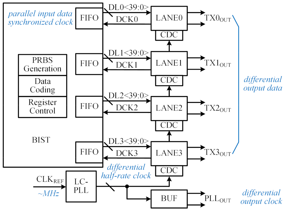
2. Top Architecture
3. Multi-Rate TX Lane Implementation
3.1. Multi-Rate Lane Timing
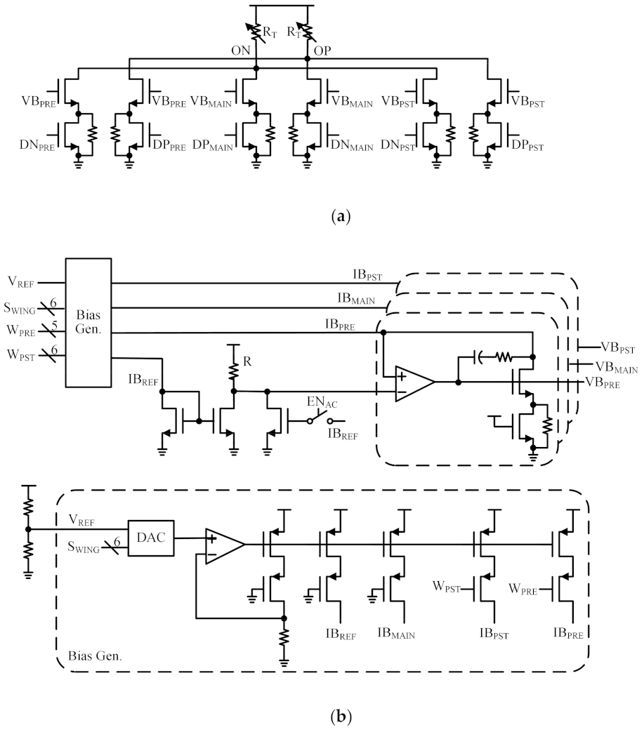
3.2. The High-Speed CML-Based Output Driver
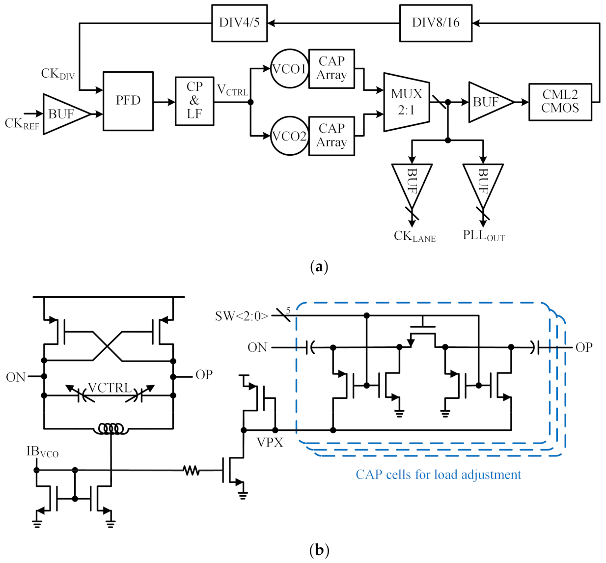
4. Wide-Operating-Range PLL
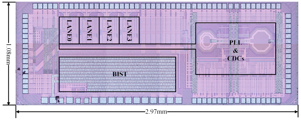
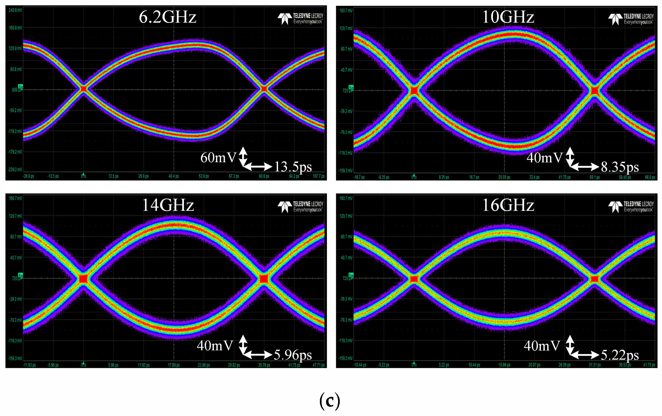
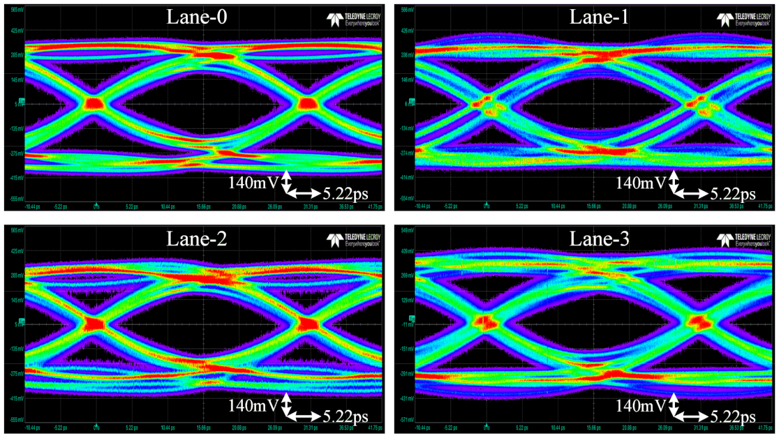
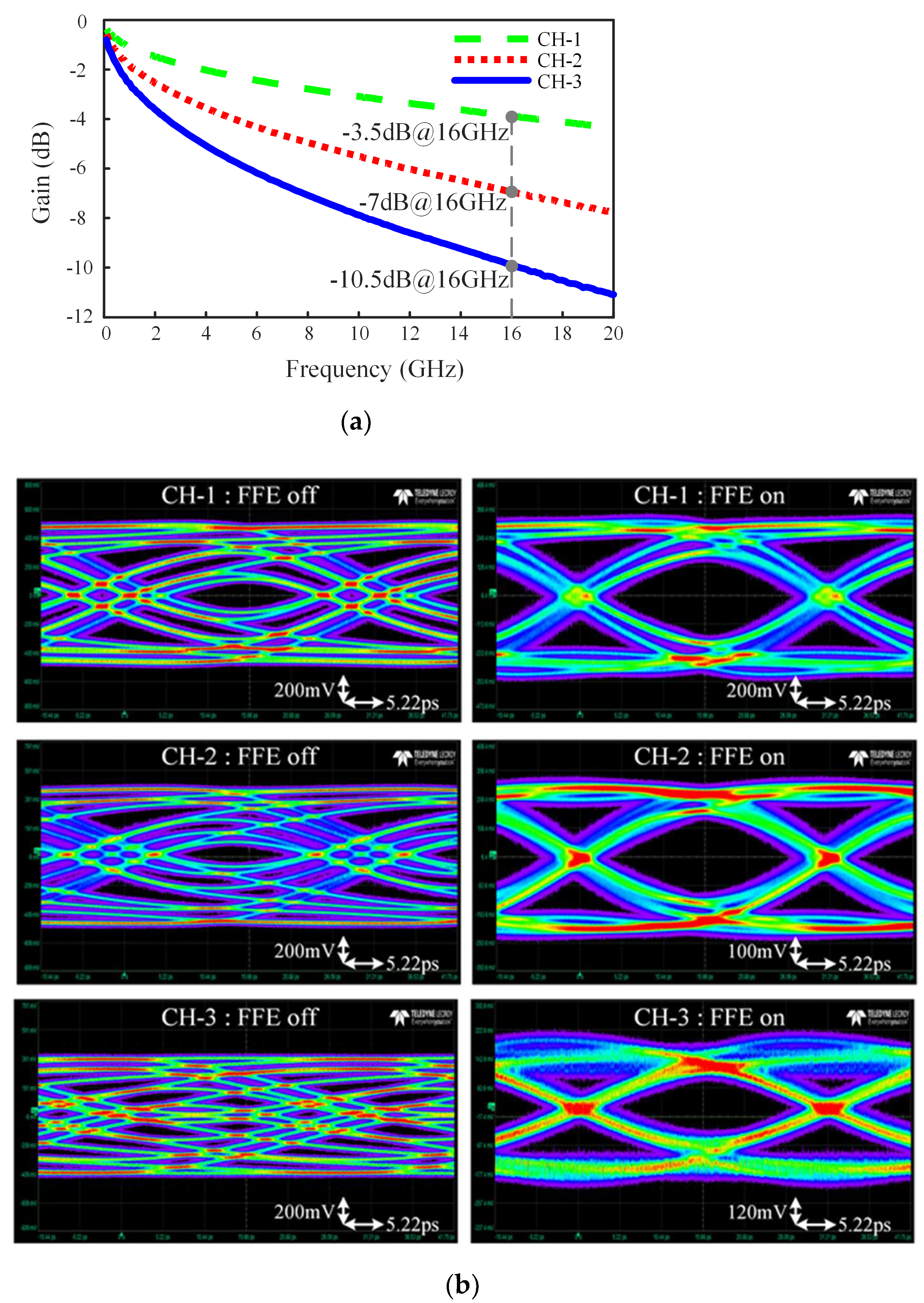
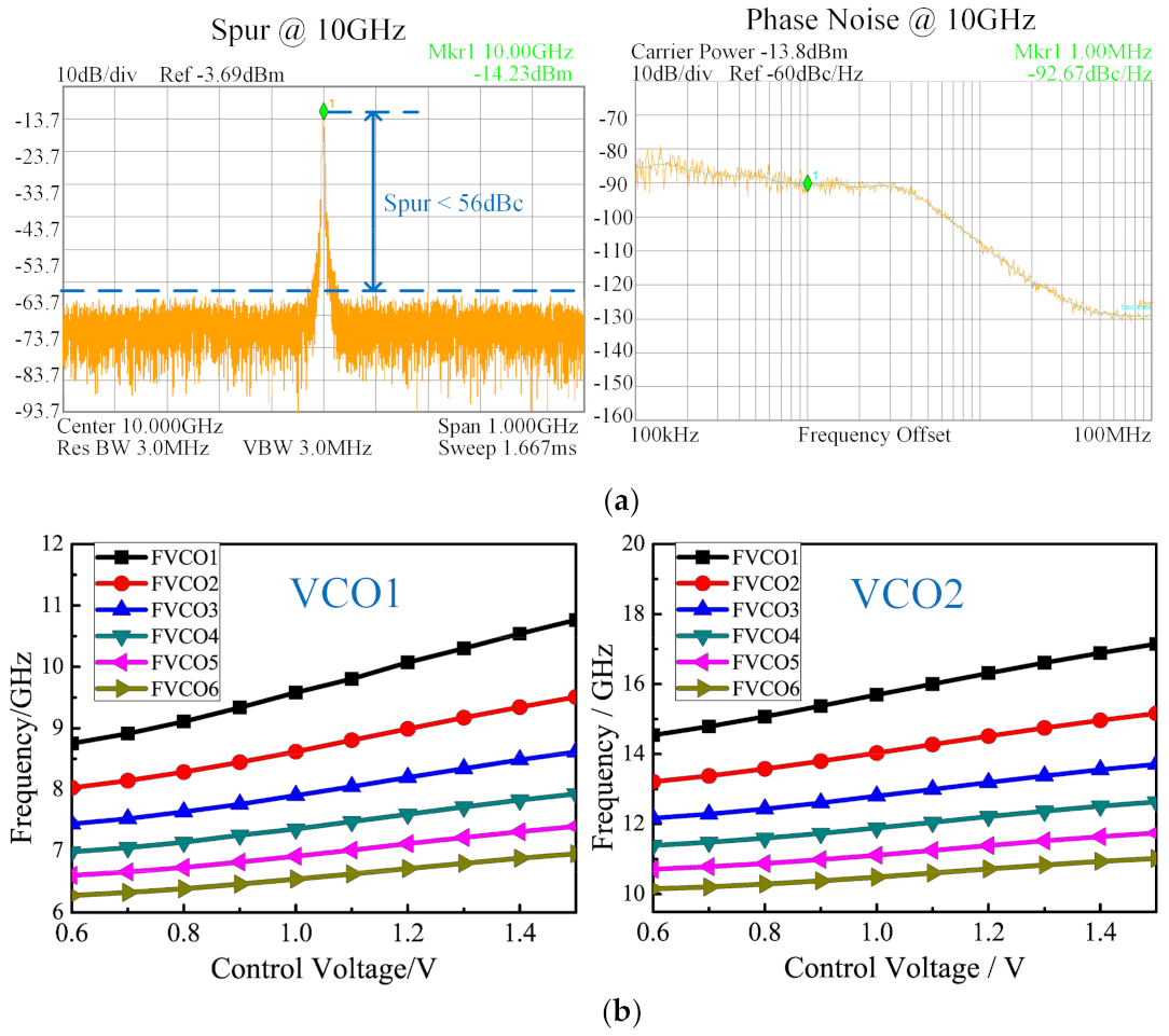
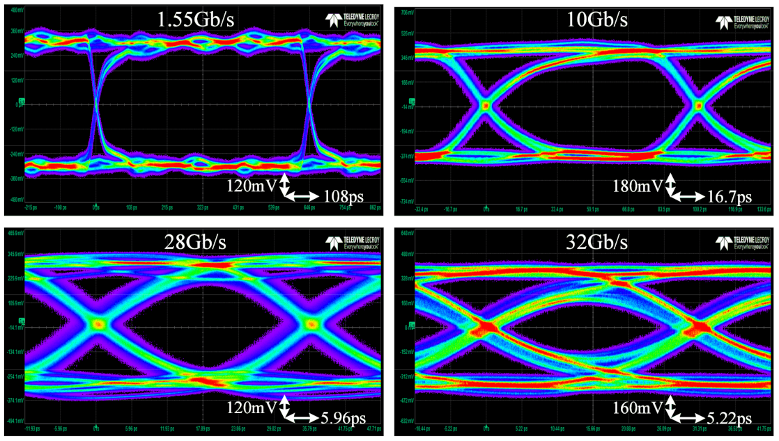
5. Measurement Results
6. Conclusions
Author Contributions
Funding
Conflicts of Interest
References
- Frans, Y.; McLeod, S.; Hedayati, H.; Elzeftawi, M.; Namkoong, J.; Lin, W.; Im, J.; Upadhyaya, P.; Chang, K. A 40-to-64 Gb/s NRZ Transmitter with Supply-Regulated Front-End in 16 nm FinFET. IEEE J. Solid-State Circuits 2016, 51, 3167–3177. [Google Scholar] [CrossRef]
- Zheng, X.; Zhang, C.; Lv, F.; Zhao, F.; Yuan, S.; Yue, S.; Wang, Z.; Li, F.; Wang, Z.; Jiang, H. A 40-Gb/s Quarter-Rate SerDes Transmitter and Receiver Chipset in 65-nm CMOS. IEEE J. Solid-State Circuits 2017, 52, 2963–2978. [Google Scholar] [CrossRef] [Green Version]
- Chen, Y.; Mak, P.I.; Boon, C.C.; Martins, R.P. A 36-Gb/s 1.3-mW/Gb/s duobinary-signal transmitter exploiting power-efficient cross-quadrature clocking multiplexers with maximized timing margin. IEEE Trans. Circuits Syst. I Regul. Pap. 2018, 65, 3014–3026. [Google Scholar] [CrossRef]
- Yuan, S.; Wu, L.; Wang, Z.; Zheng, X.; Zhang, C.; Wang, Z. A 70 mW 25Gb/s quarter-rate serdes transmitter and receiver chipset with 40 dB of equalization in 65 nm CMOS technology. IEEE Trans. Circuits Syst. I Regul. Pap. 2016, 63, 939–949. [Google Scholar] [CrossRef]
- Chen, Y.; Mak, P.I.; Zhang, L.; Qian, H.; Wang, Y. Pre-emphasis transmitter (0.007 mm2, 8 Gbit/s, 0–14 dB) with improved data zero-crossing accuracy in 65 nm CMOS. Electron. Lett. 2013, 49, 929–930. [Google Scholar] [CrossRef]
- Chen, Y.; Mak, P.; Boon, C.C.; Martins, R.P. A 27-Gb/s Time-Interleaved Duobinary Transmitter Achieving 1. 44-mW/Gb/s FOM in 65-nm CMOS. IEEE Microw. Wirel. Compon. Lett. 2017, 27, 839–841. [Google Scholar] [CrossRef]
- Zheng, X.; Zhang, C.; Lv, F.; Zhao, F.; Yue, S.; Wang, Z.; Li, F.; Jiang, H.; Wang, Z. A 4–40 Gb/s PAM4 transmitter with output linearity optimization in 65 nm CMOS. In Proceedings of the 2017 IEEE Custom Integrated Circuits Conference (CICC), Austin, TX, USA, 30 April–3 May 2017. [Google Scholar] [CrossRef]
- Yin, P.; Shu, Z.; Xia, Y.; Shen, T.; Guan, X.; Wang, X.; Mohammad, U.; Zang, J.; Fu, D.; Zeng, X.; et al. A Low-Area and Low-Power Comma Detection and Word Alignment Circuits for JESD204B/C Controller. IEEE Trans. Circuits Syst. I Regul. Pap. 2021, 68, 2925–2935. [Google Scholar] [CrossRef]
- Gao, J.; Cheng, H.; Wu, H.C.; Liu, G.; Lau, E.; Yuan, L.; Krause, C. Thunderbolt Interconnect-Opitcal and Copper. J. Light. Technol. 2017, 35, 3125–3129. [Google Scholar] [CrossRef]
- Sung, G.M.; Tung, L.F.; Wang, H.K.; Lin, J.H. USB Transceiver with a Serial Interface Engine and FIFO Queue for Efficient FPGA-to-FPGA Communication. IEEE Access 2020, 8, 69788–69799. [Google Scholar] [CrossRef]
- Bae, W.; Cho, S.Y.; Jeong, D.K. A 1.93-pj/bit pci express gen4 phy transmitter with on-chip supply regulators in 28 nm cmos. Electronics 2021, 10, 68. [Google Scholar] [CrossRef]
- Chun, Y.; Anand, T. An ISI-Resilient Data Encoding for Equalizer-Free Wireline Communication-Dicode Encoding and Error Correction for 24.2-dB Loss with 2.56 pJ/bit. IEEE J. Solid-State Circuits 2020, 55, 567–579. [Google Scholar] [CrossRef]
- Maina, R.; Tumiatti, V.; Pompili, M.; Bartnikas, R. Dielectric loss characteristics of copper-contaminated transformer oils. IEEE Trans. Power Deliv. 2010, 25, 1673–1677. [Google Scholar] [CrossRef]
- Oh, K.S. Accurate transient simulation of transmission lines with the skin effect. IEEE Trans. Comput. Des. Integr. Circuits Syst. 2000, 19, 389–396. [Google Scholar] [CrossRef]
- Chen, Y.; Mak, P.; Zhang, L.; Wang, Y. A 0.002-mm2 6.4-mW 10-Gb/s Full-Rate Direct DFE Receiver with 59.6% Horizontal Eye Opening at 10-12 BER Under 23.3-dB Channel Loss at Nyquist. IEEE Trans. Microw. Theory Technol. 2014, 62, 3107–3117. [Google Scholar] [CrossRef]
- Aroca, R.A.; Voinigescu, S.P. A large swing, 40-Gb/s SiGe BiCMOS driver with adjustable pre-emphasis for data transmission over 75 Ω coaxial cable. IEEE J. Solid-State Circuits 2008, 43, 2177–2186. [Google Scholar] [CrossRef]
- Chae, J.H.; Ko, H.; Park, J.; Kim, S. A 12.8-Gb/s Quarter-Rate Transmitter Using a 4:1 Overlapped Multiplexing Driver Combined With an Adaptive Clock Phase Aligner. IEEE Trans. Circuits Syst. II Express Briefs 2019, 66, 372–376. [Google Scholar] [CrossRef]
- Svelto, F.; Deantoni, S.; Castello, R. 1.3 GHz low-phase noise fully tunable CMOS LC VCO. IEEE J. Solid-State Circuits 2000, 35, 356–361. [Google Scholar] [CrossRef]
- Zhao, Y.; Chen, Z.; Liu, Z.; Li, X.; Wang, X. A 4.1 GHz–9.2 GHz programmable frequency divider for Ka Band pll frequency synthesizer. Electronics 2020, 9, 1773. [Google Scholar] [CrossRef]
- Hossain, M.; El-Halwagy, W.; Hossain, A.D.; Aurangozeb, A. Fractional-N DPLL-Based Low-Power Clocking Architecture for 1-14 Gb/s Multi-Standard Transmitter. IEEE J. Solid-State Circuits 2017, 52, 2647–2662. [Google Scholar] [CrossRef]
- Kim, J.; Balankutty, A.; Elshazly, A.; Huang, Y.Y.; Song, H.; Yu, K.; O’Mahony, F. A 16-to-40 Gb/s quarter-rate NRZ/PAM4 dual-mode transmitter in 14 nm CMOS. In Proceedings of the 2015 IEEE International Solid-State Circuits Conference-(ISSCC) Digest of Technical Papers, San Francisco, CA, USA, 22–26 February 2015; Volume 58, pp. 60–61. [Google Scholar] [CrossRef]
- Menoifi, C.; Braendli, M.; Francese, P.A.; Morf, T.; Cevrero, A.; Kossel, M.; Kull, L.; Luu, D.; Ozkaya, I.; Toifl, T. A 112Gb/S 2.6pJ/b 8-Tap FFE PAM-4 SST TX in 14 nm CMOS. In Proceedings of the Digest of Technical Papers-IEEE International Solid-State Circuits Conference, San Francisco, CA, USA, 11–15 February 2018; IEEE: Piscataway, NJ, USA, 2018; Volume 61, pp. 104–106. [Google Scholar]
- Roshan-Zamir, A.; Elhadidy, O.; Yang, H.W.; Palermo, S. A Reconfigurable 16/32Gb/s Dual-Mode NRZ/PAM4 SerDes in 65-nm CMOS. IEEE J. Solid-State Circuits 2017, 52, 2430–2447. [Google Scholar] [CrossRef]
- Ahn, C.; Hong, J.; Shin, J.; Kim, B.; Park, H.J.; Sim, J.Y. An 18-Gb/s NRZ Transceiver with a Channel-Included 2-UI Impulse-Response Filtering FFE and 1-Tap DFE Compensating up to 32-dB Loss. IEEE Trans. Circuits Syst. II Express Briefs 2020, 67, 2863–2867. [Google Scholar] [CrossRef]
- Choi, M.C.; Jeong, D.K.; Cho, S.Y.; Shim, M.; Kim, B.; Ko, H.G.; Ju, H.; Park, K.; Kim, H.; Kim, K. A 2.5–28 Gb/s Multi-Standard Transmitter with Two-Step Time-Multiplexing Driver. IEEE Trans. Circuits Syst. II Express Briefs 2019, 66, 1927–1931. [Google Scholar] [CrossRef]
- Bichan, M.; Ting, C.; Zand, B.; Wang, J.; Shulyzki, R.; Guthrie, J.; Tyshchenko, K.; Zhao, J.; Parsafar, A.; Liu, E.; et al. A 32Gb/s NRZ 37dB SerDes in 10nm CMOS to Support PCI Express Gen 5 Protocol. In Proceedings of the 2020 IEEE Custom Integrated Circuits Conference (CICC), Boston, MA, USA, 22–25 March 2020; pp. 19–22. [Google Scholar] [CrossRef]


| This Work | [23] | [24] | [25] | [26] | |
|---|---|---|---|---|---|
| CMOS Technology | 28 nm | 65 nm | 28 nm | 65 nm | 10 nm |
| Modulation | NRZ | NRZ/PAM-4 | NRZ | NRZ | NRZ |
| Data Rate (Gb/s) | 1.55–32 | 16/32 | 18 | 2.5–28 | 1–32 |
| FFE Tap | 3 | 4 | 3 | 3 | 5 |
| Eye Width (UI) # | 0.72 | 0.6 | N/A | 0.5 | 0.64 |
| Eye Height (V) # | 0.35 | 0.07/0.5 | 0.03 | 0.25 | 0.16 |
| Output Swing (V) # | 0.84 | 0.2/0.08 | 0.2 | 0.84 | 0.5 |
| Energy Efficiency * (pJ/bit) | 1.89 | 9.44/4.99 | 5.38 | 2.62 | 10.18 |
| Supply (V) | 0.9/1.2/1.8 | 1.2 | N/A | N/A | 1/1.8 |
| Area/Lane (mm2) | 0.048 | 0.074 | 0.021 | 0.196 | 0.24 |
Publisher’s Note: MDPI stays neutral with regard to jurisdictional claims in published maps and institutional affiliations. |
© 2021 by the authors. Licensee MDPI, Basel, Switzerland. This article is an open access article distributed under the terms and conditions of the Creative Commons Attribution (CC BY) license (https://creativecommons.org/licenses/by/4.0/).
Share and Cite
Cai, C.; Zheng, X.; Chen, Y.; Wu, D.; Luan, J.; Lu, D.; Zhou, L.; Wu, J.; Liu, X. A 1.55-to-32-Gb/s Four-Lane Transmitter with 3-Tap Feed Forward Equalizer and Shared PLL in 28-nm CMOS. Electronics 2021, 10, 1873. https://doi.org/10.3390/electronics10161873
Cai C, Zheng X, Chen Y, Wu D, Luan J, Lu D, Zhou L, Wu J, Liu X. A 1.55-to-32-Gb/s Four-Lane Transmitter with 3-Tap Feed Forward Equalizer and Shared PLL in 28-nm CMOS. Electronics. 2021; 10(16):1873. https://doi.org/10.3390/electronics10161873
Chicago/Turabian StyleCai, Chen, Xuqiang Zheng, Yong Chen, Danyu Wu, Jian Luan, Dechao Lu, Lei Zhou, Jin Wu, and Xinyu Liu. 2021. "A 1.55-to-32-Gb/s Four-Lane Transmitter with 3-Tap Feed Forward Equalizer and Shared PLL in 28-nm CMOS" Electronics 10, no. 16: 1873. https://doi.org/10.3390/electronics10161873
APA StyleCai, C., Zheng, X., Chen, Y., Wu, D., Luan, J., Lu, D., Zhou, L., Wu, J., & Liu, X. (2021). A 1.55-to-32-Gb/s Four-Lane Transmitter with 3-Tap Feed Forward Equalizer and Shared PLL in 28-nm CMOS. Electronics, 10(16), 1873. https://doi.org/10.3390/electronics10161873