Article

A 50.5 ns Wake-Up-Latency 11.2 pJ/Inst Asynchronous Wake-Up Controller in FDSOI 28 nm

CEA, LETI, MINATEC Campus, F-38054 Grenoble, France
*
Author to whom correspondence should be addressed.
J. Low Power Electron. Appl. 2019, 9(1), 8; https://doi.org/10.3390/jlpea9010008
Submission received: 7 December 2018 / Revised: 6 February 2019 / Accepted: 7 February 2019 / Published: 14 February 2019

Abstract

:
Due to low activity in Internet of Things (IoT) applications, systems tend to leverage low power modes in order to reduce their power consumption. Normally-off computing thus arose, consisting in having turned off most part of a system’s power supply, while dynamically turning on components as the application needs it. As wake up sources may be diverse, simple controllers are integrated to handle smart wake up schemes. Therefore, to prevent overconsumption while transitioning to running mode, fast wake up sequences are required. An asynchronous 16-bit Reduced Instruction Set Computer (RISC) Wake-up Controller (WuC) is proposed demonstrating 50.5 [email protected] Million Instructions Per Second (MIPS)@0.6 V wake-up latency, drastically reducing the overall wake-up energy of IoT systems. A clockless implementation of the controller saves the booting time and the power consumption of a clock generator, while providing high robustness to environmental variations such as supply voltage level. The WuC is also able to run simple tasks with a reduced Instruction Set Architecture (ISA) and achieves as low as 11.2 pJ/inst @0.5 V in Fully Depleted Silicon On Insulator (FDSOI) 28 nm.

1. Introduction

In order to reduce the power consumption of Internet of Things (IoT) applications and due to low activity schedule for the nodes of such applications, low power modes have been integrated in microcontrollers. Reducing the clock frequency or the supply voltage level is an efficient way to obtain low power systems for the IoT [1]. Pushing this idea to the end by halting the clock and powering off most parts of the system, normally-off computing means that a system is turned on only when it has to realize a given task [2]. Wake up sources vary and may also be unpredictable, requiring a smart controller to handle the wake-up process. Big/little architectures thus appeared where high performance processors and peripherals are turned on upon request [3]. The little controller performances are paramount and determine the overall power consumption since the system mainly remains in low power modes. In this paper, we leverage asynchronous design techniques which natively remove the clocking and timing constraints while providing high robustness to system environment variations [4].
Low energy IoT applications require low leakage during idle mode and high energy efficiency during computing phases. Idle mode is defined thereafter as a state where a processor is not active but ready to shift into high power execution mode. For a synchronous processor, in idle mode, the clock is kept running at a low frequency to avoid booting the clock generator by switching it on. Previously proposed IoT microcontroller subsystems still suffer from high power consumption in idle mode, due to time-keepers and always-on sub-blocks. When in deep sleep or idle modes, these systems still suffer from high wake-up latencies preventing them from significant power reduction opportunities during applicative sleep phases [5]. We define wake-up latency as the time between an external event and the first fetch of an instruction within the node core controller. This latency represents a time slot where the system may consume close to active state power consumption, while not processing, since it is waking up. For energy concerns, a short wake-up latency is paramount for tasks that are small enough to be tackled by the little processor alone (e.g., activity logging, lightweight processing).
We propose, in this paper, an asynchronous 16-bit Reduced Instruction Set Computer (RISC) Wake-up Controller (WuC) demonstrating fast wake-up latency and managing simple tasks using a reduced Instruction Set Architecture (ISA). It is a processor core associated with a 4 kB Static Random Access Memory (SRAM) memory. As no time keepers are needed in asynchronous implementations, this WuC achieves 50.5 ns latency to wake up from idle mode, running at 9.2 Million Instructions Per Second (MIPS).
As shown in Figure 1, a wireless sensor node controller can be partitioned into an Arm Cortex M0+ on the one hand and the proposed Wake-up Controller on the other hand. The WuC manages simple node tasks and wakes up the M0+ using a dedicated signal only when a complex computation is required. The M0+ is thus in deep sleep mode and the system does not suffer from high wake-up latencies, saving a lot of energy in burst mode of operation.
In our system, an Arm Cortex M0+ subsystem in Fully Depleted Silicon On Insulator (FDSOI) 28 nm is integrated on our test board along with the WuC subsystem circuit to demonstrate the functionality of the whole big/little system. The M0+ subsystem integrates a Cortex M0+ and a 256 kB SRAM connected through a Light Advanced High-performance Bus (AHB-Lite) matrix. In a typical application, the M0+ subsystem is turned off most of the time and the WuC subsystem is in idle mode, waiting for incoming events. The asynchronous processor has incoming external wake up signals which may come from various sources such as wake-up radios [6] or sensors. It then executes the appropriate routine, may execute a program on its own, or wake up the bigger processor to handle the task. This paper focuses on the wake-up controller rather than the design of the components which generate interruption signals. These components, such as wake up radio receivers, may increase the whole system power consumption, especially in idle state, but are not part of this work since their presence in the system is highly application dependent.
In the second section, the proposed asynchronous processor architecture is first described and measurement results are then presented. The third section discusses the results in the frame of the state-of-the-art. Section 4 details the materials and methods which have been used.

2. Results

In this section, the architecture of the proposed asynchronous circuit is detailed. Measurement results after fabrication are then presented.

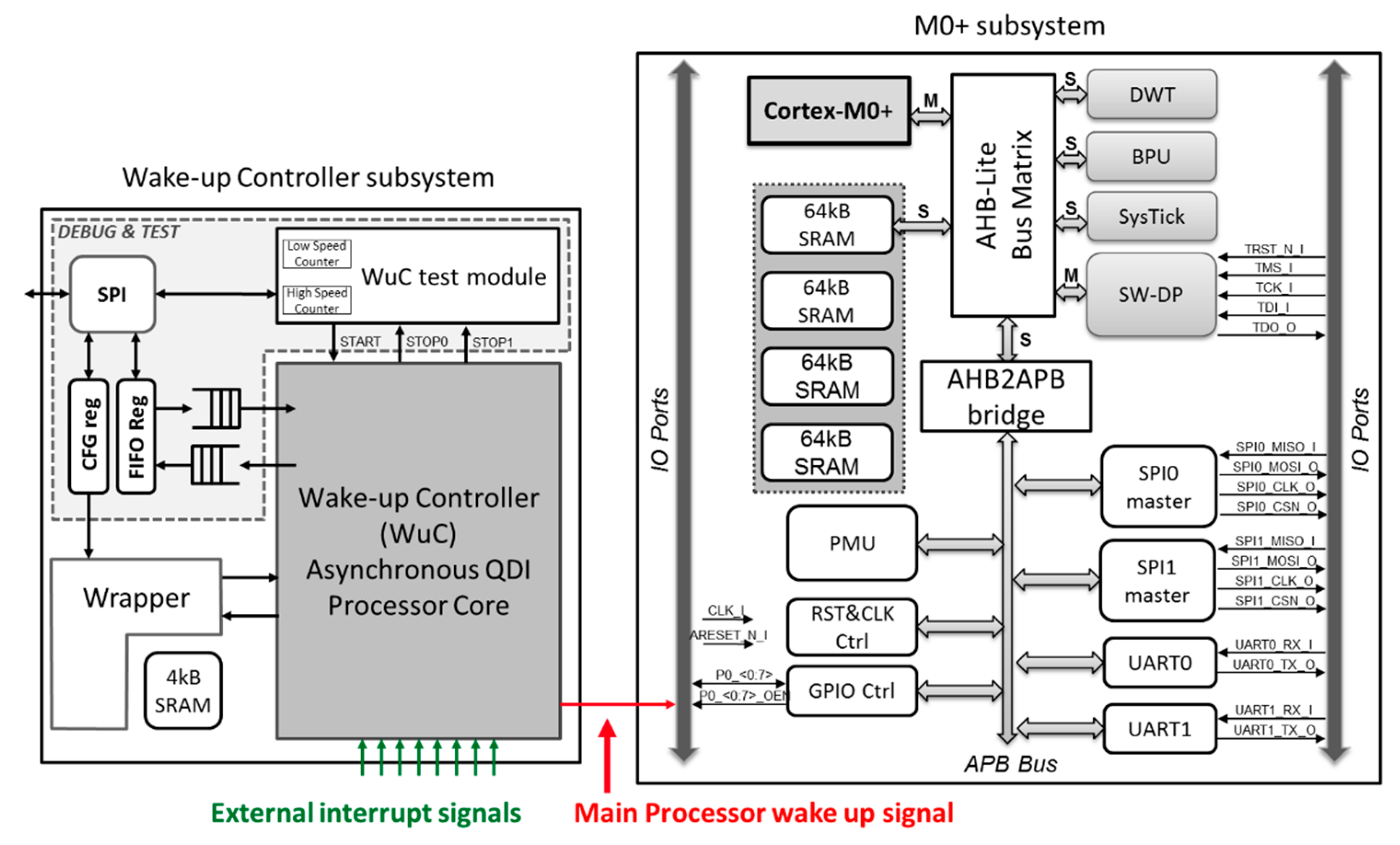
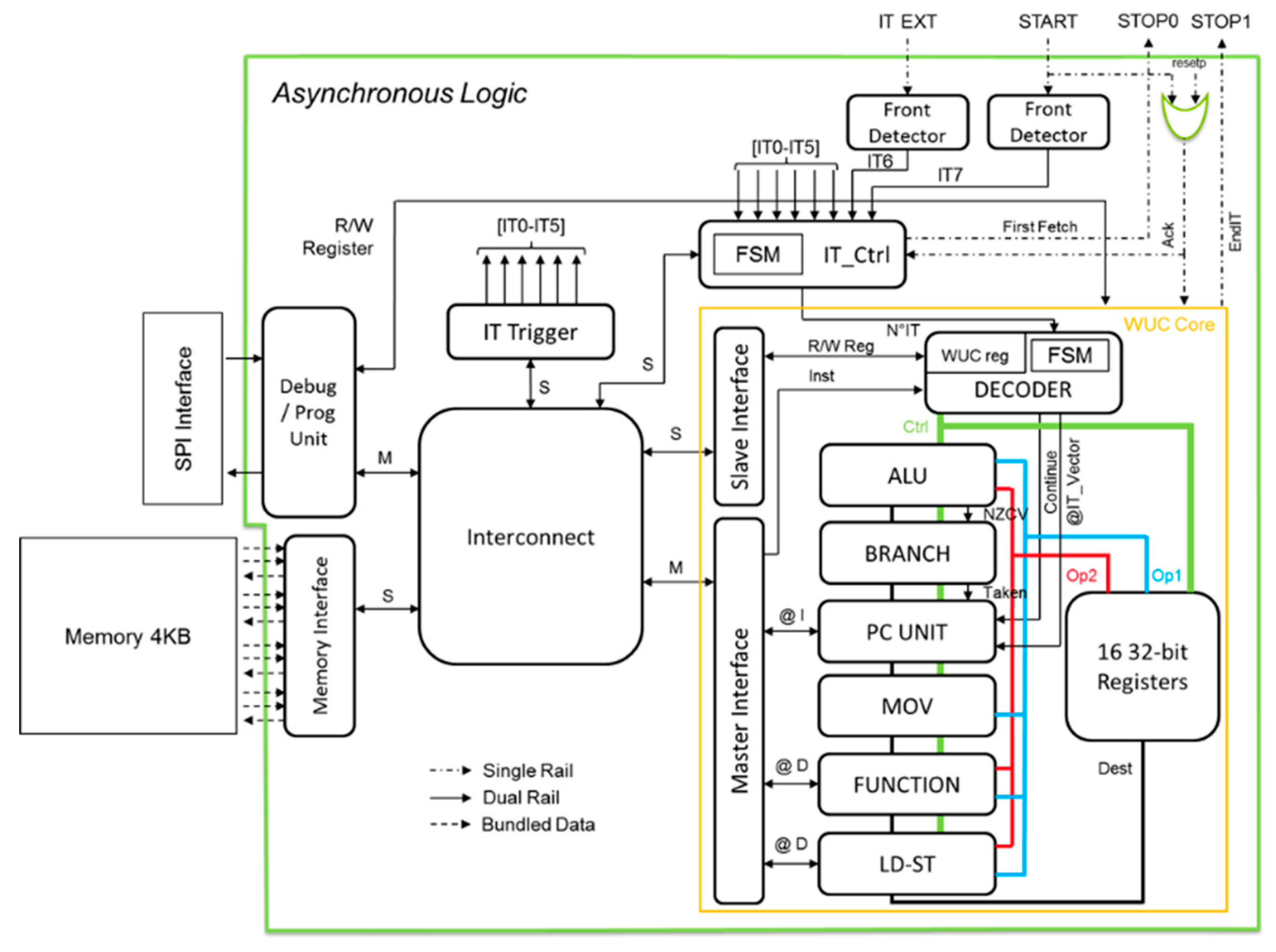
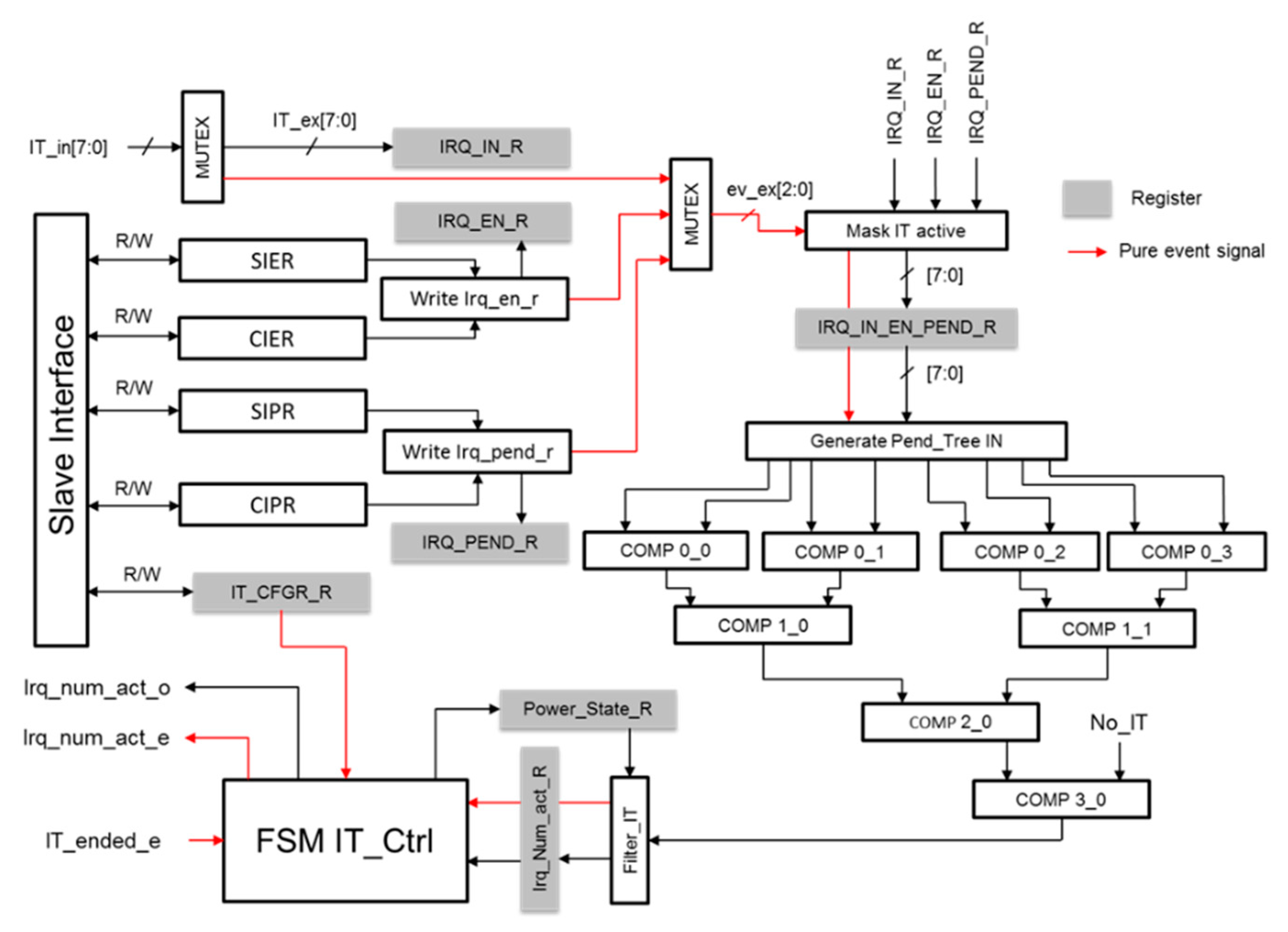
2.1. Asynchronous Wake up Controller Architecture

While usual synchronous designs use a clock signal to trigger data processing within a circuit, asynchronous design uses a handshake protocol to implement a clockless data-driven processing scheme [7]. Among the variety of self-timed circuits implementation types, Quasi-Delay-Insensitive (QDI) are those which operate correctly independently of the delays in gates and wires. The only timing constraint which exists is the isochronic-fork assumption, which prevents from hazardous behavior within the circuit [8]. The event-driven scheme provides robustness to operating parameters such as temperature, supply voltage level, or process variations, while implementing automatic sleep mode (i.e., clock-gated mode in synchronous circuits). These advantages make asynchronous QDI circuits highly suitable for low power applications such as the Internet of Things [9]. While the dual-rail encoding is used to implement the four-phase handshake protocol, mixing data and request, bundled-data implementation may be used to allow lighter binary encoding. This compromise is possible at the cost of additional timing constraints between the data signals, which have to be valid, and the request signal, which handles the protocol along with the acknowledgement signal. Since the least constraints set is targeted, dual rail implementation is used in most parts of the design, except for large busses like the memory interface.
The proposed asynchronous WuC (Figure 2) implements a compact 16-bit Instruction Set Architecture (ISA) based on load/store RISC instructions and a 32-bit data path. It has been chosen to perform simple tasks as described in an Ultra Low Power Bench (ULPBench). A dedicated C compiler has been developed and is used to program the Interrupt Service Routines (ISR) to be executed. A 16-bit address is used to be compliant with a small 4 kB SRAM memory (program, data, IT vector) and thus save power accordingly. This memory and all the masters and slaves are connected through an asynchronous interconnect. A debug unit has been developed and is able to program, read/write, all address space and registers. It also has the capability to manage stop, run, and step commands for usual debug during code execution. Sixteen 32-bit general purpose registers including Stack Pointer, Link Register and Program Counter (PC) are integrated. An Interrupt controller module (IT_Ctrl) receives interrupt signals (ITs) from up to 8 internal or external peripherals and indicates to the WuC core which IT to execute.
The core is asynchronous and thus naturally in idle mode until an IT event occurs at its input. Once evaluated, the IT vector address is sent to the Program Counter (PC) Unit. The IT vector content is thus loaded from the memory, through a specific asynchronous wrapper. Instructions are sent to the decoder unit and distributed to the five execution units (Arithmetic and Logic Unit (ALU), BRANCH, MOV, Load-Store unit (LD-ST) and FUNCTION) and to data path controllers. Data processing is independently executed in each unit where it is needed and the PC unit is waiting for their completion. As the execution units are arranged concurrently, and thanks to the data-driven behavior of asynchronous circuits, no scheduler is needed to manage the pipeline sequence. The correct propagation of data within the circuits is ensured by the request/acknowledge handshake protocol. This protocol, along with the rest of the processing, is implemented using both standard cells and asynchronous-specific cells such as the C-element.
The interrupt controller (Figure 3) is a key module to demonstrate very fast wake up. This module is in charge of managing and sorting incoming events according to their IT number. To improve wake up and interrupt routine execution latencies, no preemption is possible; the ISR are executed until completion. Incoming interrupts are asynchronous single rail channels consisting of a request signal and an acknowledgement signal. They satisfy the handshake protocol by maintaining their request signal active until the interrupt has been acknowledged. Following the four phases protocol, they then switch to inactive and will at least wait until the acknowledgement signal is deasserted to send a new IT event. To manage simultaneous IT events, a MutEx (Mutual Exclusion module) is used and a specific register ‘irq_in_r’ is updated accordingly. Furthermore, it is possible to enable/disable some IT inputs through a slave register interface connected to the local interconnect. Finally, a ‘irq_in_en_pend_r’ register stores IT events information and their relative status. At this step, and to determine which IT number/priority occurred, a comparator tree is implemented (COMPxy). An asynchronous event is thus generated to the finite state machine unit and only sent to the WuC core if inactive—no preemption possible.

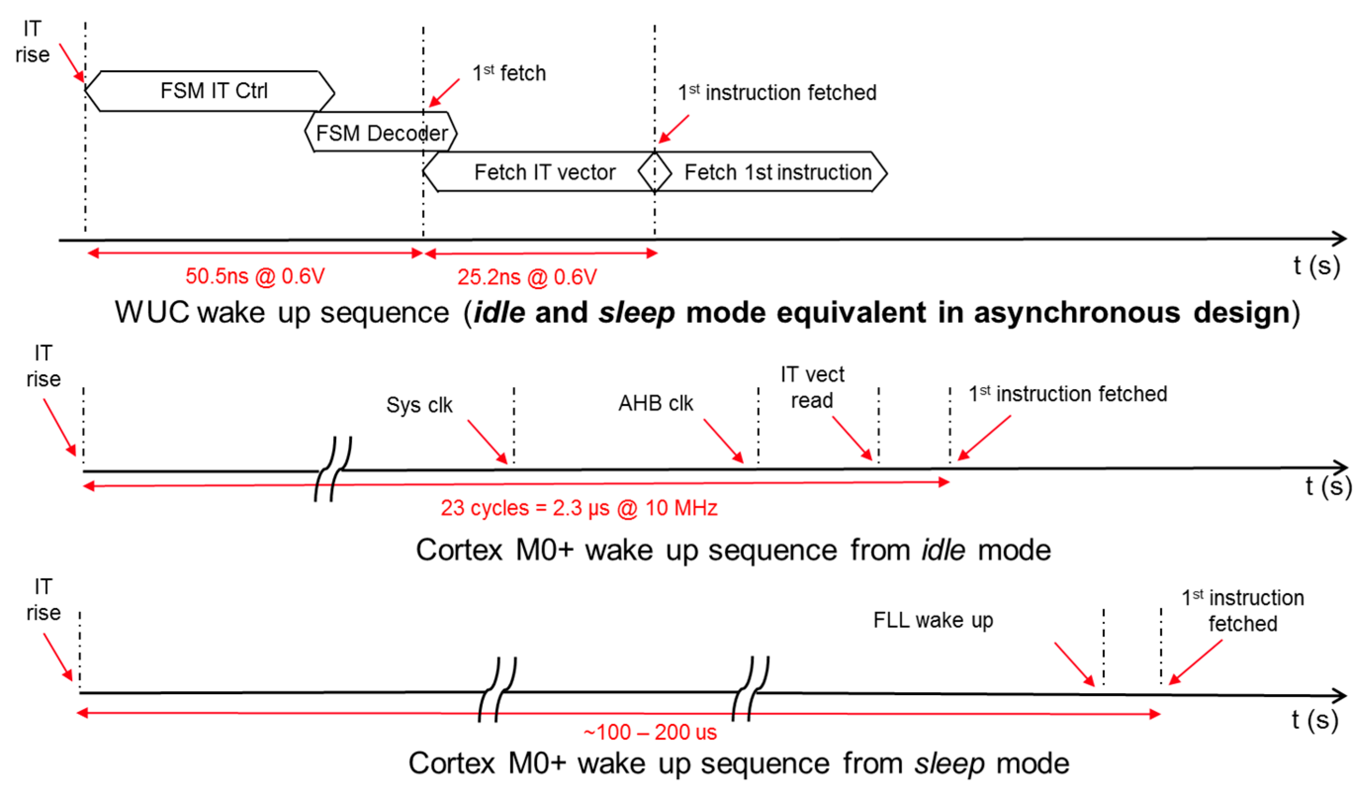
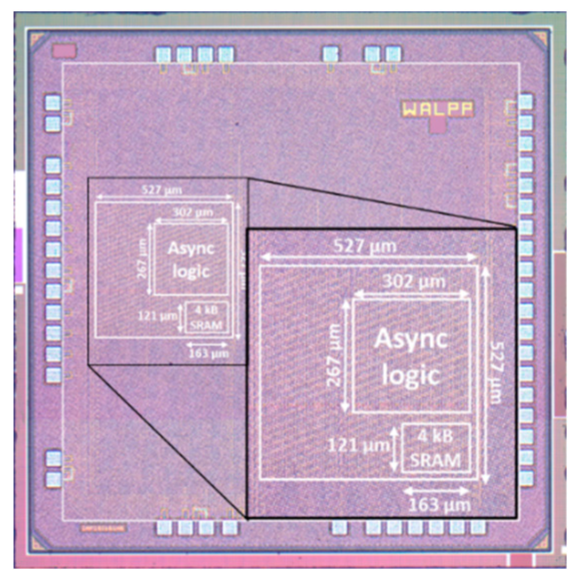
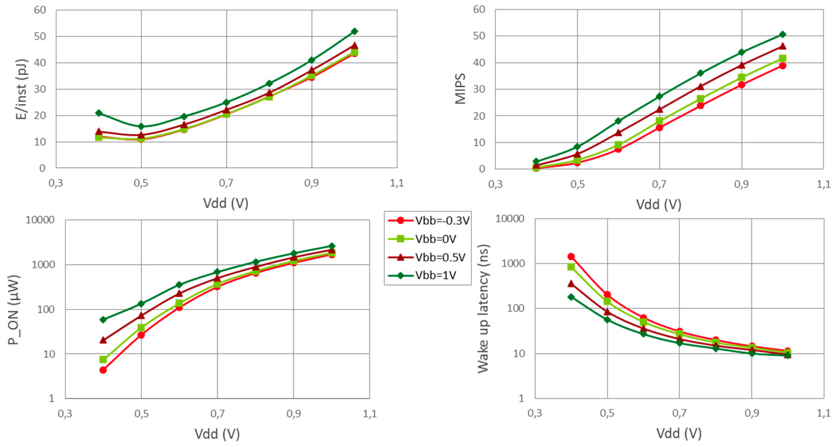
2.2. Measurement Results

To estimate the WuC performance results, a specific program has been developed executing 2018 instructions and generating 2912 memory accesses. Figure 4 shows a timing diagram corresponding to different wake-up execution steps. For the asynchronous WuC, the idle mode is a functional mode due to clockless design and natural clock gating. The WuC exhibits 8.8 µ[email protected] V idle mode power consumption and takes 50.5 [email protected] MIPS to wake-up from idle mode. M0+ wake-up latency from idle mode is 23 cycles, i.e., 2.3 μs@10 MHz and more than 100 µs to wake-up from sleep mode. To achieve similar M0+ wake up latency, the system clock would need to run at a significantly higher frequency at the cost of a higher power consumption.
The WuC has been fabricated in FDSOI 28 nm technology (Figure 5). Power supplies have been properly isolated in order to determine the power consumption and performances of the controller while avoiding power consumption from miscellaneous components such as test-oriented modules or asynchronous/synchronous memory wrapper. The asynchronous Wake-up Controller exhibits 3.5 to 50.6 MIPS in the 0.5–1 V supply voltage level (VDD) range and 0–1 V bias voltage level (VBB) range.
As shown in Figure 6, the minimum energy point is 11.2 pJ/[email protected] V. Static power consumed by the logic core is 5.6 µW and total dynamic power 39 µW at 0.5 V VDD without back bias. In the end, the proposed asynchronous WuC exhibits more than 45x gain in wake-up latency compared to M0+ running at the same frequency, which validates our approach.

3. Discussion

Contrary to other approaches (Table 1) requiring voltage regulators and clock generators, the proposed asynchronous WuC can start-up at very low voltage without requiring any stable voltage supply. In our system, the WuC power grid is directly connected to the external world. While for characterization, a laboratory power supply has been used to power the controller, the circuit may be directly plugged to any power supply that satisfies the voltage limits of the technology process cell libraries.
In any case [5,10,11], the WuC wake-up latency to recover from idle mode is drastically reduced with regard to the state-of-the-art by one to two decades for similar energy performances. In our applicative scenario, M0+ goes into sleep to save energy and is woken up only when complex computing tasks are required. We could then extend our system to use a more powerful core like Arm Cortex-M3 or Arm Cortex-M4.

4. Materials and Methods

Materials which were used for this work consist in FDSOI 28 nm technology process Platform Design Kit (PDK) from STMicroelectronics. To implement the WuC, we used the following cell libraries:
  • 12 tracks Standard Cells implemented with Low Threshold Voltage transistors.
  • Standard digital I/O cells supplied with 1.8 V external power supply.
  • Bitcells from the Bitcell Reference Library
Moreover, asynchronous-dedicated cells belonged to a specific library, which were also provided following a specific request. It included C-elements, Half-Buffers, Mutex elements for the asynchronous core but also Synchronizers and Sequencers to implement asynchronous/synchronous interfaces. In the asynchronous cell library, which was provided in ST 28 nm FDSOI technology, the cells used a semi-static implementation, which reduces the area.
Regarding the methods, the following methods and tools have been used in the following order:
  • RTL description of the whole circuit. For the asynchronous part, similar description exists and describes asynchronous token transfers through communication channels [12].
  • Logical synthesis has been performed, using ACC for the asynchronous part [12] and using Design Compiler from Synopsys for the rest of the chip. The asynchronous logical synthesis, which was performed by ACC, consists of the following:
    • Deriving the rules for data events (also known as tokens) generation from the provided asynchronous-specific HDL description;
    • Implementing the netlist of gates which satisfy these rules;
    • Locating the isochronic forks and performing a timing analysis to generate a set of minimum and maximum delay constraints between gates inputs and outputs which satisfies the isochronic fork assumption [8].
  • Physical Implementation was realized with SoC Encounter from Cadence. (a specific add-on has been provided by STMicroelectronics for implementation optimization for FDSOI 28 nm). Regarding the implementation of the asynchronous parts, the timing constraints issued from synthesis were used to optimize, place and route the gates netlist in order to ensure the correct operation of the asynchronous design.
  • Physical verification and signoff have been done with Calibre from Mentor Graphics.

Author Contributions

Conceptualization, J.F.C., F.B. and E.B.; methodology, J.F.C., I.M.-P. and F.H.; software, F.B., F.H. and O.D.; validation, J.F.C., I.M.-P., E.G. and Y.T.; formal analysis, S.T. and Y.T.; investigation, J.F.C., F.B. and E.B.; resources, E.B. and P.V.; data curation, A.M.; writing—original draft preparation, J.F.C., F.B. and E.B.; writing—review and editing, J.F.C. and D.C.; supervision, E.B.; project administration, E.B. and A.V.; funding acquisition, E.B.

Funding

This research was partially funded by the THINGS2DO project (JTI Contract Number 621221).

Conflicts of Interest

The authors declare no conflict of interest. The funders had no role in the design of the study; in the collection, analyses, or interpretation of data; in the writing of the manuscript; or in the decision to publish the results.

References

  1. Myers, J.; Savanth, A.; Howard, D.; Gaddh, R.; Prabhat, P.; Flynn, D. An 80nW retention 11.7pj/cycle active subthreshold ARM cortex-M0+ subsystem in 65nm CMOS for WSN applications. In Proceedings of the 2015 IEEE International Solid-State Circuits Conference—(ISSCC) Digest of Technical Papers, San Francisco, CA, USA, 22–26 February 2015. [Google Scholar]
  2. Hayashikoshi, M.; Sato, Y.; Ueki, H.; Kawai, H.; Shimizu, T. Normally-off MCU architecture for low-power sensor node. In Proceedings of the 2014 IEEE 19th Asia and South Pacific Design Automation Conference (ASP-DAC), Singapore, 20–23 January 2014. [Google Scholar]
  3. Zhu, Y.; Reddi, V.J. High-performance and energy-efficient mobile web browsing on big/little systems. In Proceedings of the 2013 IEEE 19th International Symposium on High Performance Computer Architecture (HPCA), Shenzhen, China, 23–27 February 2013. [Google Scholar]
  4. Otero, C.T.O.; Tse, J.; Karmazin, R.; Hill, B.; Manohar, R. ULSNAP: An ultra-low power event-driven microcontroller for sensor network nodes. In Proceedings of the Fifteenth International Symposium on Quality Electronic Design, Santa Clara, CA, USA, 3–5 March 2014. [Google Scholar]
  5. TI CC2650 SimpleLink Multistandard Wireless MCU. Available online: http://www.ti.com/lit/ds/symlink/cc2650.pdf (accessed on 30 November 2018).
  6. Piyare, R.; Murphy, A.L.; Kiraly, C.; Tosato, P.; Brunelli, D. Ultra Low Power Wake-Up Radios: A hardware and Networking Survey. IEEE Commun. Surv. Tutor. 2017, 19, 2117–2157. [Google Scholar] [CrossRef]
  7. Martin, A.J.; Nystrom, M. Asynchronous Techniques for System-on-Chip Design. Proc. IEEE 2006, 94, 1089–1120. [Google Scholar] [CrossRef] [Green Version]
  8. Nowick, S.M.; Singh, M. Asynchronous Design—Part 1: Overview and Recent Advances. IEEE Des. Test 2015, 32, 5–18. [Google Scholar] [CrossRef]
  9. Beigne, E.; Vivet, P.; Thonnart, Y.; Christmann, J.F.; Clermidy, F. Asynchronous Circuit Designs for the Internet of Everything: A Methodology for ultralow-Power Circuits with GALS Architecture. IEEE Solid State Circuits Mag. 2016, 8, 39–47. [Google Scholar] [CrossRef]
  10. Myers, J.; Savanth, A.; Prabhat, P.; Yang, S.; Gaddh, R.; Toh, S.O.; Flynn, D. A 12.4pJ/cycle sub-threshold, 16pJ/cycle near-threshold ARM Cortex-M0+ MCU with autonomous SRPG/DVFS and temperature tracking clocks. In Proceedings of the 2017 Symposium on VLSI Circuits, Kyoto, Japan, 5–8 June 2017. [Google Scholar]
  11. Paul, S.; Honkote, V.; Kim, R.; Majumder, T.; Aseron, P.; Grossnickle, V.; Sankman, R.; Mallik, D.; Jain, S.; Vangal, S.; et al. An energy harvesting wireless sensor node for IoT systems featuring a near-threshold voltage IA-32 microcontroller in 14nm tri-gate CMOS. In Proceedings of the 2016 IEEE Symposium on VLSI Circuits (VLSI-Circuits), Honolulu, HI, USA, 15–17 June 2016. [Google Scholar]
  12. Renaudin, M.; Fonkoua, A. Tiempo Asynchronous Circuits System Verilog Modeling Language. In Proceedings of the 2012 IEEE 18th International Symposium on Asynchronous Circuits and Systems, Lyngby, Denmark, 7–9 May 2012. [Google Scholar]
Figure 1. Wireless sensor node microcontroller subsystem: Wake up Controller and M0+ partitions.
Jlpea 09 00008 g001
Figure 2. Asynchronous Wake up Controller micro-architecture.
Jlpea 09 00008 g002
Figure 3. Interrupt controller (IT_Ctrl) micro-architecture.
Jlpea 09 00008 g003
Figure 4. Code execution timing diagram for Wake-up Controller in idle (i.e., sleep) mode. M0+ wake up sequences in idle/sleep modes.
Jlpea 09 00008 g004
Figure 5. Wake-up controller chip micrograph. The chip has been fabricated in Ultra-Thin Body Bias (UTBB) FDSOI 28 nm from STMicroelectronics using Low Voltage Threshold (LVT) transistors-based gates. The die core area is 0.278 mm². The supply voltage range is from 0.4 V to 1 V while the back-biasing voltage range is from −0.3 V to 1 V.
Jlpea 09 00008 g005
Figure 6. Wake-up Controller measurement results versus supply voltage level. Graphs illustrate Energy/inst (top-left), MIPS (top-right), wake up latency (bottom-left) and dynamic power (bottom-right).
Jlpea 09 00008 g006
Table 1. Wake up Controller performances summary and state-of-the-art comparison.
WuC (This work)VLSI 2016 [8]VLSI 2017 [7]TI CC2650 [5]
ProcessFDSOI 28nm LVT14nm Tri Gate CMOS65nm CMOS-
Core Vdd Range0.4–1V0.308–1V0.3–1.2V-
Logic TypeAsynchronousSynchronousSynchronousSynchronous
CPU16-bit RISC32-bit Intel Architecture32-bit ARM Cortex M0+ARM Cortex M3
ARM Cortex M0
Sensor Ctrl 16 bits
Data path32 bits32 bits32 bitsSensor Controller
16 bits
Memory4 KB LVT SRAM16KB Boot ROM
64KB SRAM
8KB DTCM
8KB I$
12KB LV RAM, RTC, PMU, GPIO, Debug, SPI, 128b AES, DMA, 2KB ROM, IVR, scan, BISTSensor Controller
2KB SRAM
Frequency Range3.5-50.6 MIPS500KHz–297MHz12kHz–60MHzSensor Ctrl
24MHz max
Idle power5.6 µW @ 0.5V-120uW 4KB + CPU @ 46nW20KB SRAM + CPU + Sensor Ctrl + 2KB SRAM + RTC @ 1µA (retention)
Emin11.2pJ/[email protected]
4MIPS
17pJ/cycle
@ 0.37V, 3.5MHz
26pJ/cycle
@ 0.6V, 100MHz
6.3pJ @ 0.35V, 174kHz 12.44 pJ/cycle @ 0.6V, 10.5MHz-
Wake Up Latency50.5 ns @ 9.7MIPS
from Idle mode
~µs from short sleep
~ ms from long sleep
~s from deepsleep
µs-ms151 µs from Standby Mode
1015 µs from Shutdown Mode
Power ModesRun, IdleNo Sleep, Short Sleep, Long Sleep, Deep SleepRun, SRPG/DFVS, Retention, SleepActive, Idle, Stanby, Shutdown
Debug UnitYesYesYesYes

