A Survey of Low Voltage and Low Power Amplifier Topologies

 ,
, 
Abstract
:1. Introduction
2. Amplifier Topologies
2.1. Inverter Based Amplifier
2.1.1. Tunable Inverter-Based Amplifier
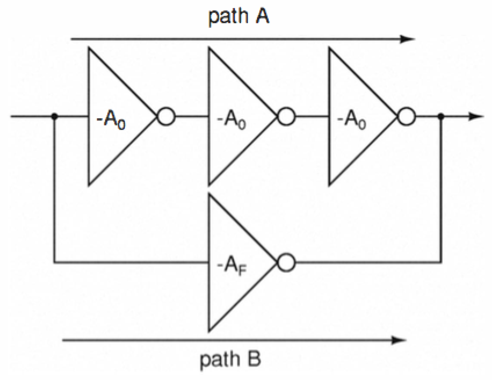
2.1.2. Inverter-Based Amplifier with Feed-Forward Compensation
2.1.3. Current-Starved Inverter-Based Amplifier
2.2. Bulk-driven Ampliifer
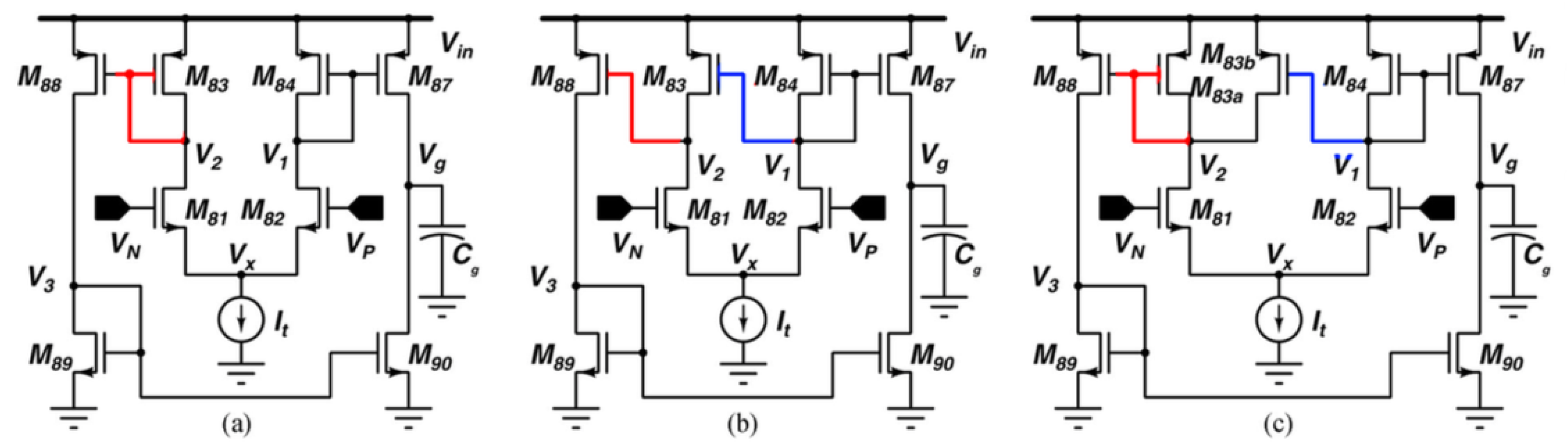
2.3. Hybrid Mode Amplifier
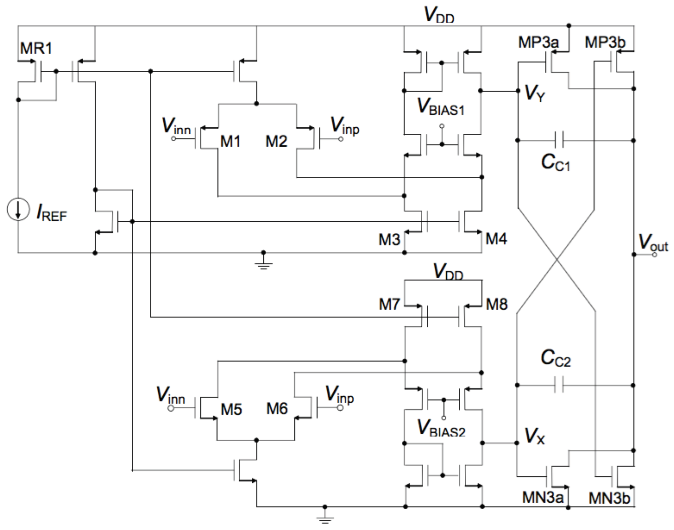
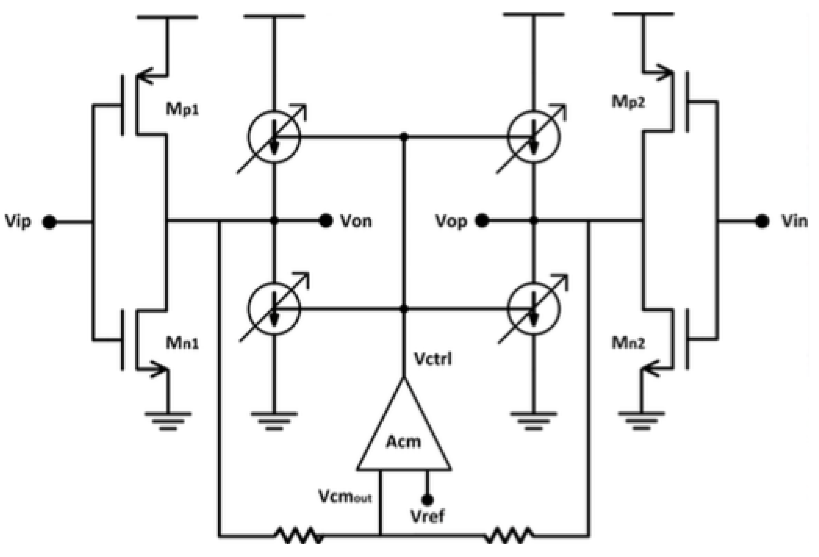
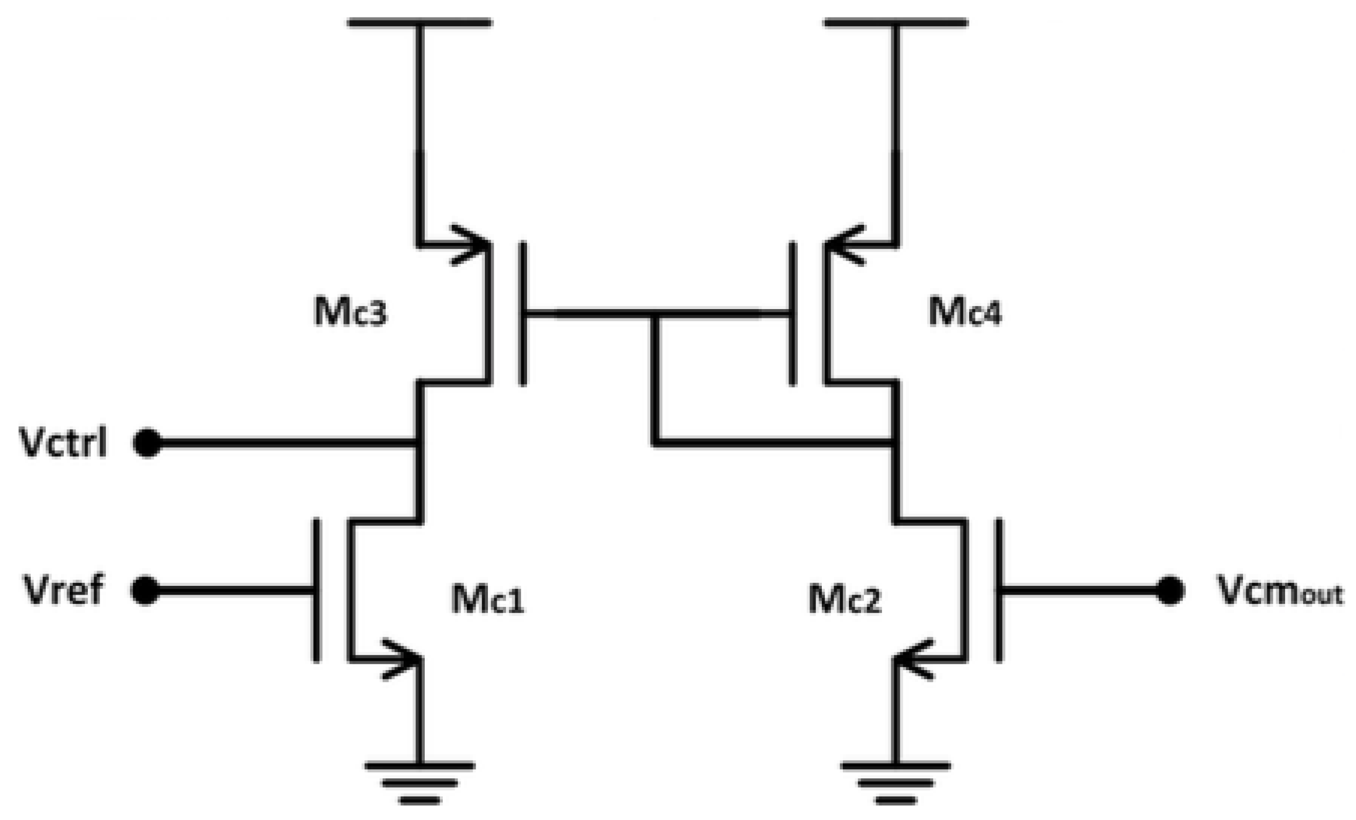
2.4. Rail-to-Rail Amplifier with Cross-Coupled Output Stage
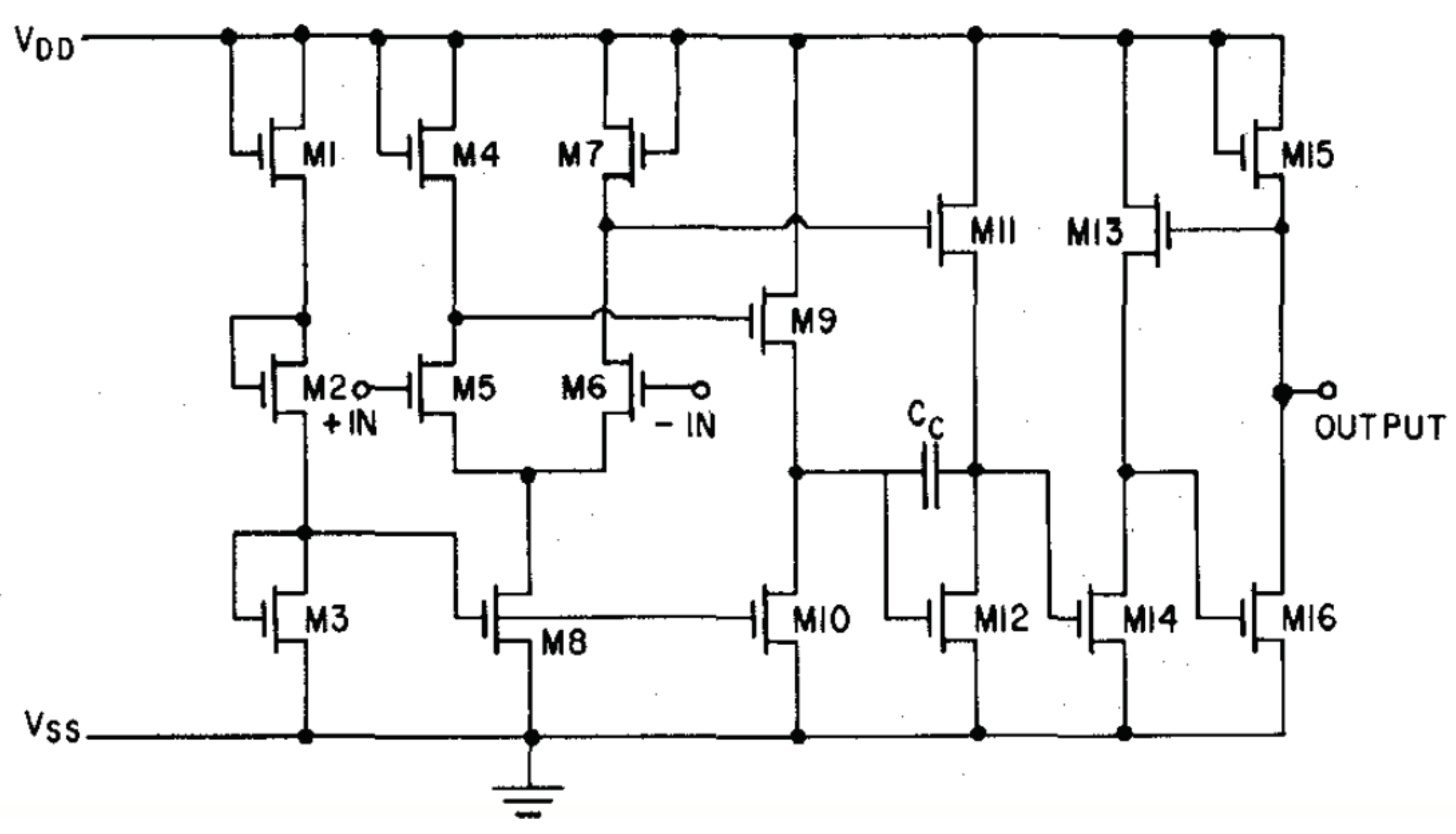
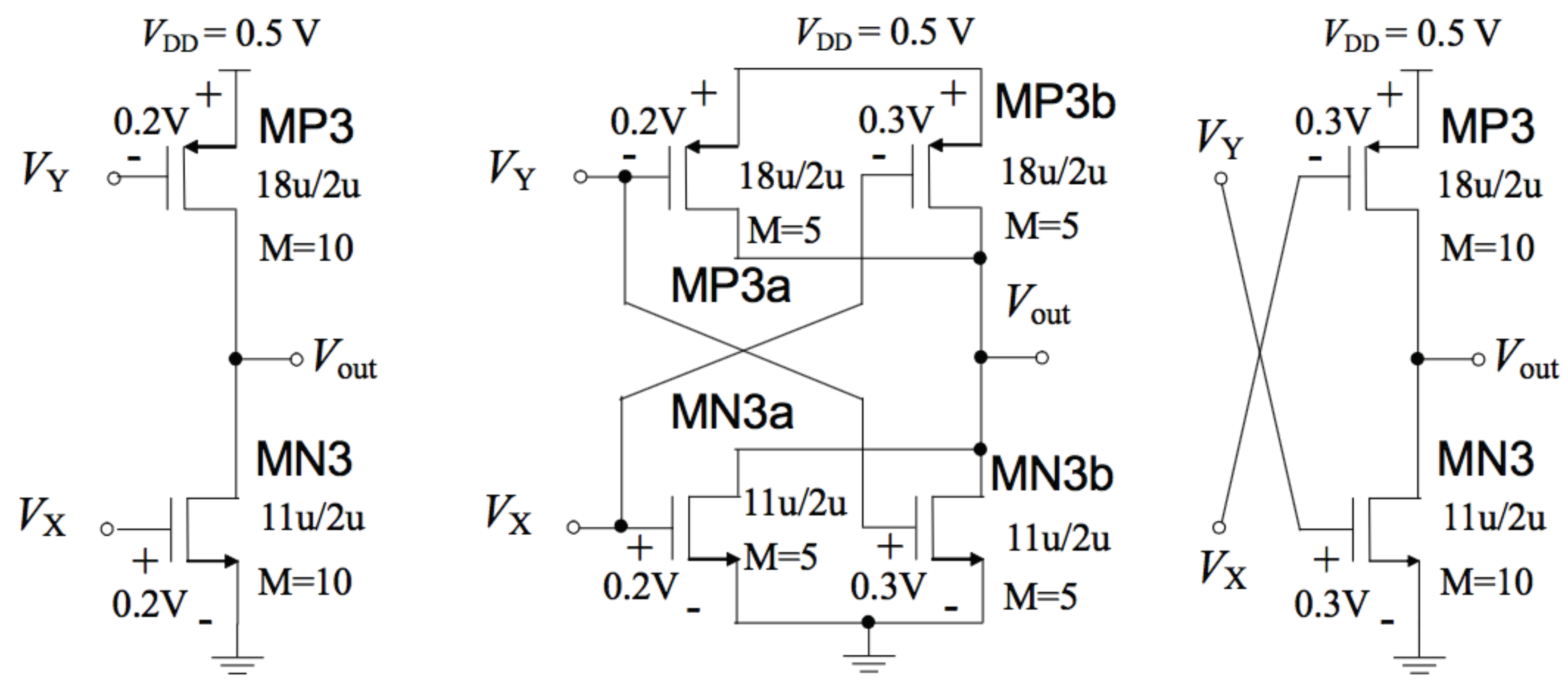
2.5. NMOS-Only Amplifier
3. Results and Comparison
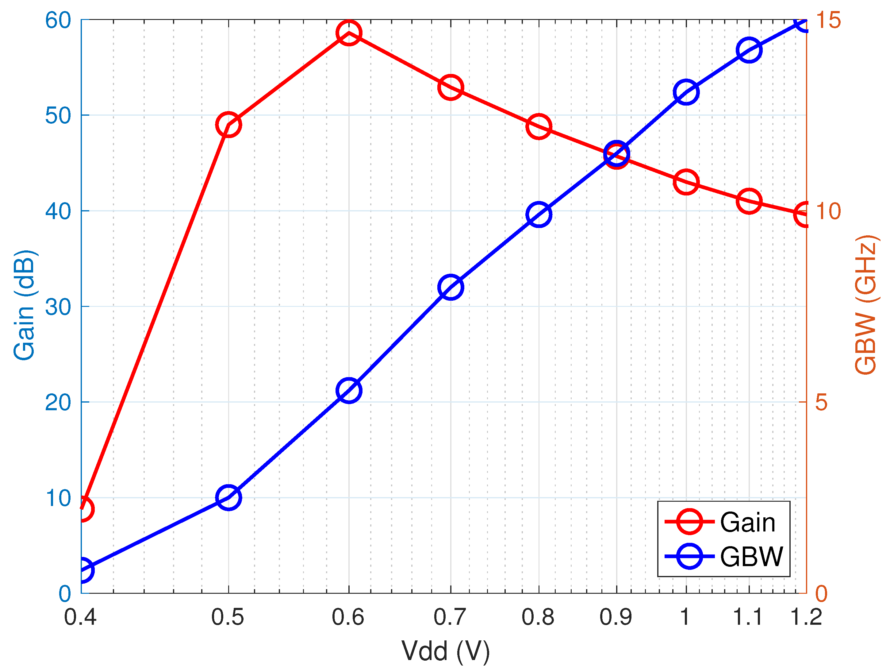
3.1. Tunable Inverter-Based Amplifier
3.2. Inverter-Based Amplifier with Feed-Forward Compensation
3.3. Current-Starved Inverter-Based Amplifier
3.4. Bulk-Driven Amplifier
3.5. Hybrid-Mode Amplifier
3.6. Rail-To-Rail Amplifier with Cross-Coupled Output Stage
3.7. NMOS-only Amplifier
4. Discussion
5. Conclusions
Author Contributions
Funding
Conflicts of Interest
Abbreviations
| CMOS | Complementary Metal Oxide Semiconductor |
| UMC | United Microelectronics Corporation |
| OTA | Operational Transconductance Amplifier |
| CM | Common Mode |
| GBW | Gain Bandwidth |
| PM | Phase Margin |
| CMFB | Common Mode Feedback |
| CMRR | Common Mode Rejection Ratio |
| PSRR | Power Supply Rejection Ratio |
| FOM | Figure Of Merit |
References
- Ismail, A.; Mostafa, I. A Process-Tolerant, Low-Voltage, Inverter-Based OTA for Continuous-Time ADC. IEEE TVLSI 2016, 24, 2911–2917. [Google Scholar]
- Shrimali, H.; Chatterjee, S. 11 GHz UGBW Op-amp with feed-forward compensation technique. In Proceedings of the IEEE International Symposium of Circuits and Systems (ISCAS), Rio de Janeiro, Brazil, 15–18 May 2011; pp. 17–20. [Google Scholar]
- Coccoli, A.; Richelli, A.; Redouté, J.M. EMI Susceptibility of a Digitally Based Analog Amplifier in a 180-nm CMOS Process. IEEE TEMC 2016, 58, 1236–1239. [Google Scholar] [CrossRef]
- Bazes, M. Two novel fully complementary self-biased CMOS differential amplifiers. IEEE JSSC 1991, 26, 165–168. [Google Scholar] [CrossRef]
- Wilson, W.; Chen, T.; Selby, R. A Current-Starved Inverter-Based Differential Amplifier Design for Ultra-Low Power Applications. In Proceedings of the 2013 IEEE 4th Latin American Symposium on Circuits and Systems (LASCAS), Cusco, Peru, 27 February–1 March 2013; pp. 1–4. [Google Scholar]
- Ferreira, L.H.C.; Pimenta, T.C.; Moreno, R.L. An Ultra-Low-Voltage Ultra-Low-Power CMOS Miller OTA With Rail-to-Rail Input/Output Swing. IEEE TCAS-II 2007, 54, 843–847. [Google Scholar] [CrossRef]
- Kim, T.-W. A-250 mV supply-voltage 65 dB-gain OTA with an enhanced bandwidth and a reduced compensation-capacitor. In Proceedings of the 2018 International Conference on Electronics, Information, and Communication (ICEIC), Honolulu, HI, USA, 24–27 January 2018; pp. 1–4. [Google Scholar]
- Maity, A.; Patra, A. A Hybrid-Mode Operational Transconductance Amplifier for an Adaptively Biased Low Dropout Regulator. IEEE TPEL 2017, 32, 1245–1254. [Google Scholar] [CrossRef]
- Qin, Z.; Tanaka, A.; Takaya, N.; Yoshizawa, H. 0.5-V 70-nW Rail-to-Rail Operational Amplifier Using a Cross-Coupled Output Stage. IEEE TCAS-II 2016, 63, 1009–1013. [Google Scholar] [CrossRef]
- Young, I.A. A High-performance All-Enhancement NMOS Operational Amplifier. IEEE JSSC 1979, 14, 1070–1077. [Google Scholar] [CrossRef]
- Sbaraini, S.; Richelli, A.; Kovacs-Vajna, Z.M. EMI susceptibility in bulk-driven Miller opamp. IET EL 2010, 46, 1111–1113. [Google Scholar] [CrossRef]
- Venturelli, M.; Torricelli, F.; Ghittorelli, M.; Colalongo, L.; Richelli, A.; Kovács-Vajna, Z.M. Unipolar Differential Logic for Large-Scale Integration of Flexible a-IGZO Circuits. IEEE TCAS-II 2017, 64, 565–569. [Google Scholar]
- Kundu, R.; Pandey, A.; Ghosh, D.; Singh, J.; Nath, V. A 4.596 GHz, High Slew Rate, Ultra low Power Cascode Operational Amplifier in 45 nm CMOS for Wireless Communication. Int. J. Comput. Appl. Eng. Sci. 2014, 3, 15–20. [Google Scholar]
- Far, A. Amplifier for energy harvesting: Low voltage, ultra low current, rail-to-rail input-output, high speed. In Proceedings of the 2016 IEEE International Autumn Meeting on Power, Electronics and Computing (ROPEC), Ixtapa, Mexico, 9–11 November 2016. [Google Scholar]
- Kulej, T. 0.5-V bulk-driven OTA and its applications. Int. J. Circ. Theor. Appl. 2015, 43, 187–204. [Google Scholar] [CrossRef]
- O’uchi, S. 0.8-V Rail-to-Rail Operational Amplifier with Near Vt Gain-Boosting Stage Fabricated in FinFET Technology for IoT Sensor Nodes. In Proceedings of the 2015 IEEE SOI-3D-Subthreshold Microelectronics Technology Unified Conference (S3S), Rohnert Park, CA, USA, 5–8 October 2015. [Google Scholar]
- Chang, J.; Zhang, X.; Ge, T.; Zhou, J. Fully printed electronics on flexible substrates: High gain amplifiers and DAC. Org. Electron. 2014, 15, 701–710. [Google Scholar] [CrossRef]


| Width [m] | Lenght [m] | Finger Number | |
|---|---|---|---|
| Mn1, Mn2 | 100 | 2 | 10 |
| Mp1, Mp2 | 350 | 2 | 24 |
| Mi1, Mi2 | 4 | 2 | 2 |
| Mi3, Mi4 | 16 | 2 | 2 |
| Mc1, Mc2 | 1 | 4 | 2 |
| Mc3, Mc4 | 4 | 4 | 2 |
| Vdd | Gain | GBW | PM |
|---|---|---|---|
| 0.4 V | 8.8 dB | 0.6 GHz | 120 |
| 0.5 V | 49 dB | 2.5 GHz | 46 |
| 0.6 V | 58.6 dB | 5.3 GHz | 18 |
| 0.7 V | 52.9 dB | 8 GHz | 30 |
| 0.8 V | 48.8 dB | 9.9 GHz | 39 |
| 0.9 V | 45.7 dB | 11.5 GHz | 48 |
| 1 V | 43 dB | 13.1 GHz | 55 |
| 1.1 V | 41 dB | 14.2 GHz | 60 |
| 1.2 V | 39.6 dB | 15 GHz | 65 |
| Width [m] | Lenght [m] | Finger Number | |
|---|---|---|---|
| nMOS1 | 2 | 1 | 2 |
| pMOS1 | 4 | 1 | 8 |
| nMOS2 | 2 | 4 | 4 |
| pMOS2 | 1 | 2 | 2 |
| nMOS3 | 3 | 3 | 6 |
| pMOS3 | 1 | 2 | 2 |
| N-CMFB | 5.5 | 7.5 | 1 |
| P-CMFB | 3 | 1 | 1 |
| Vdd | 1.1 V | 0.9 V | 0.7 V |
| 53 dB | 65 dB | 74 dB | |
| GBW | 3.6 MHz | 2 MHz | 208 kHz |
| Load | 15 pF | 6 pF | 1.8 pF |
| Phase margin | 90 | 90 | 90 |
| CMRR | 233 dB | 180 dB | 211 dB |
| Power consumption | 21 W | 3 W | 137 nW |
| Width [m] | Lenght [m] | Finger Number | |
|---|---|---|---|
| Q1, Q2 | 2.4 | 0.6 | 2 |
| Q3a, Q4a | 1.5 | 0.6 | 2 |
| Q3b, Q4b | 4.5 | 0.6 | 2 |
| QP, Q5 | 2.4 | 0.6 | 2 |
| Q6 | 6 | 0.6 | 2 |
| Q7 | 12 | 0.6 | 2 |
| Q8, Q9 | 1.8 | 0.6 | 2 |
| Width [m] | Lenght [m] | Finger Number | |
|---|---|---|---|
| M81, M82 | 10 | 1 | 2 |
| M84,M87, M88 | 90 | 1 | 4 |
| M83a, M83b | 45 | 1 | 2 |
| M89, M90 | 30 | 1 | 8 |
| Width [m] | Lenght [m] | Finger Number | |
|---|---|---|---|
| M1, M2 | 18 | 2 | 4 |
| M3,M4 | 11 | 2 | 4 |
| M5, M6 | 11 | 2 | 4 |
| M7, M8 | 18 | 2 | 4 |
| MN3a, MN3b | 44 | 2 | 4 |
| MP3a, MP3b | 72 | 2 | 4 |
| MB1a, MB1b | 11 | 2 | 4 |
| MB2a, MB2b | 18 | 2 | 4 |
| NM1, NM2 | 11 | 2 | 1 |
| PM1, PM2, PM3 | 18 | 2 | 1 |
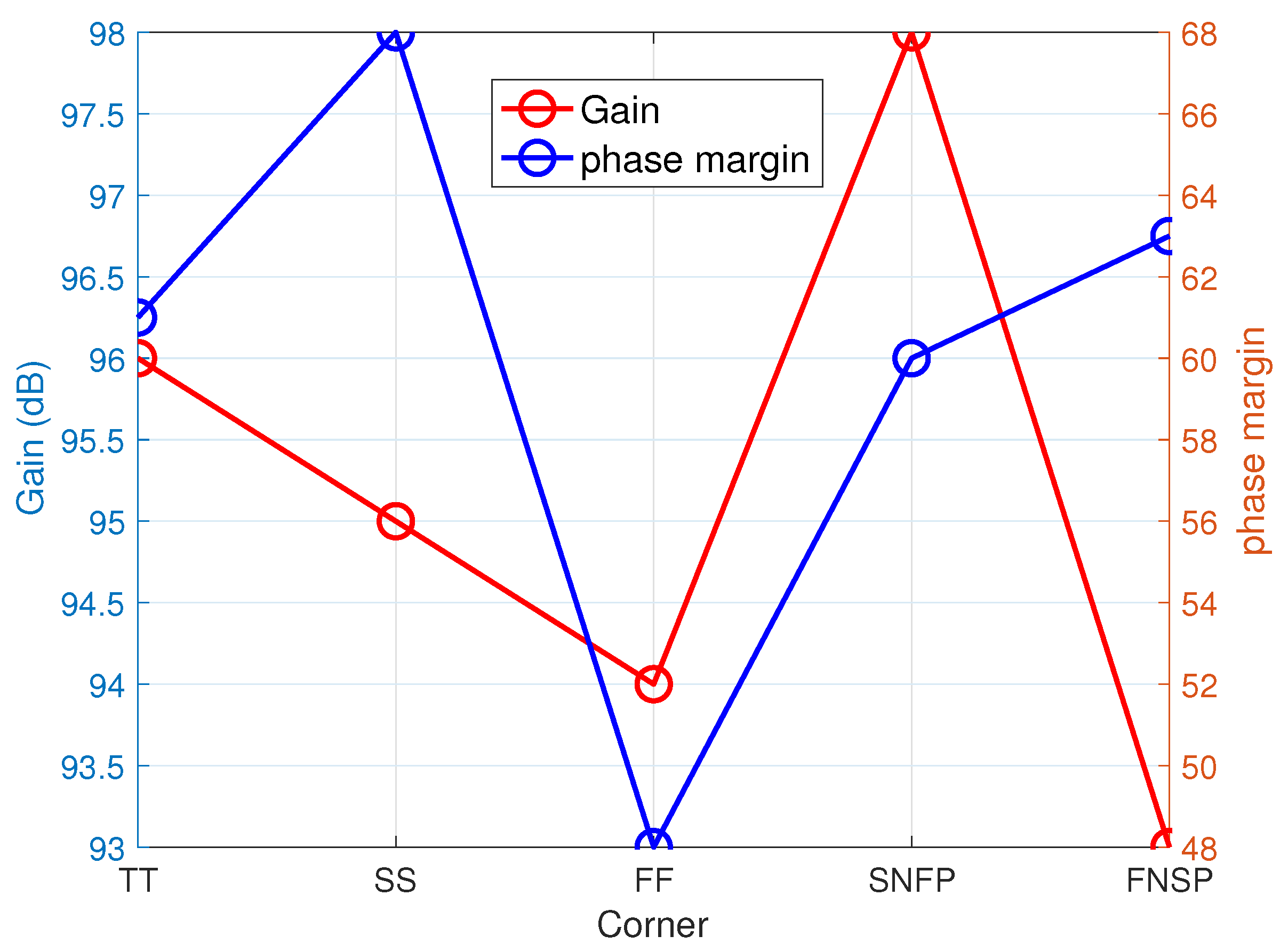
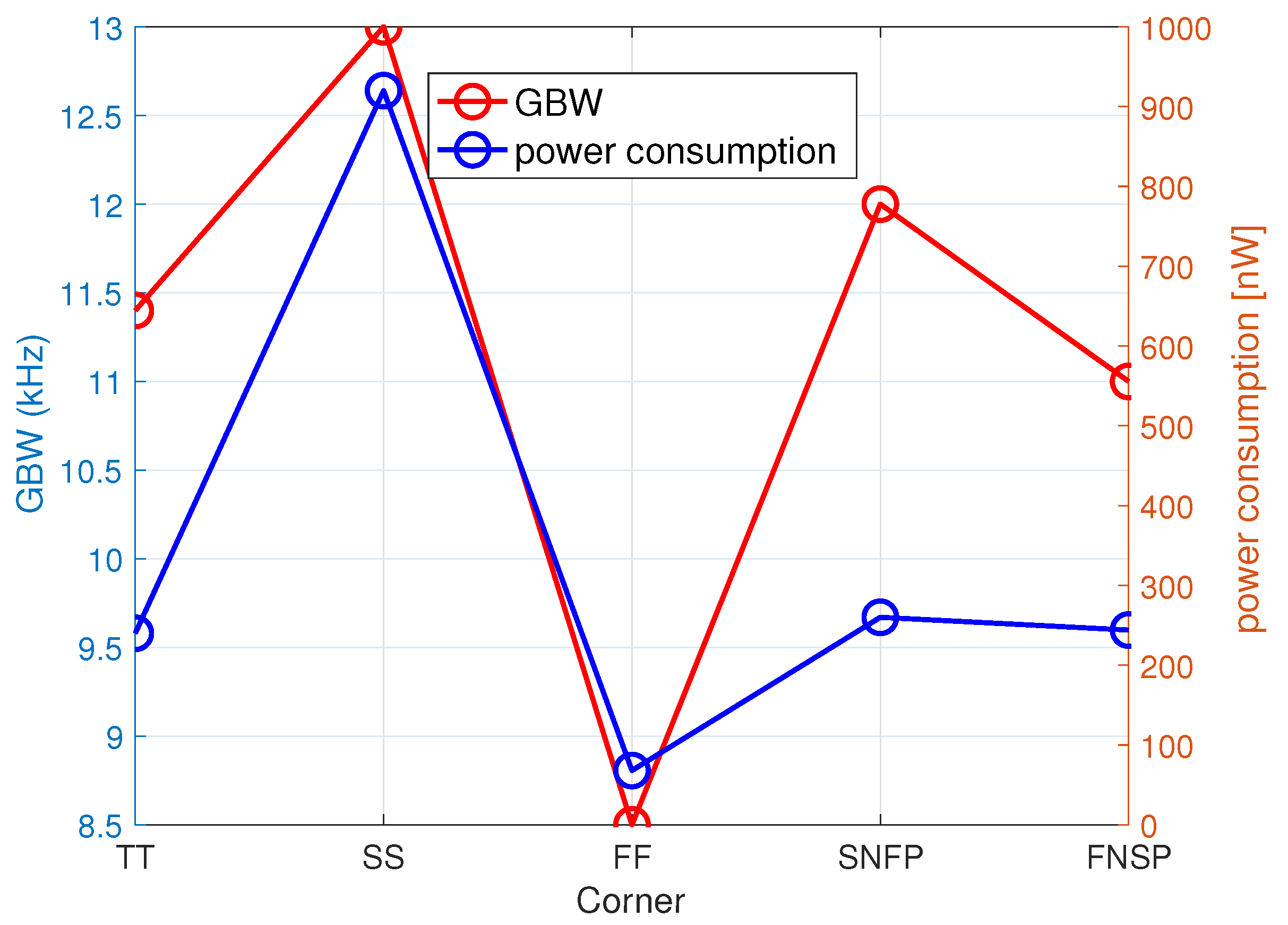
| Gain | GBW | PM | Power Consumption | |
|---|---|---|---|---|
| TT | 96 dB | 11.4 kHz | 61 | 240 nW |
| FF | 95 dB | 13 kHz | 68 | 920 nW |
| SS | 94 dB | 8.5 kHz | 48 | 68 nW |
| SNFP | 98 dB | 12 kHz | 60 | 260 nW |
| FNSP | 93 dB | 11 kHz | 63 | 244 nW |
| Width [m] | Lenght [m] | Finger Number | |
|---|---|---|---|
| M1 | 42 | 0.5 | 6 |
| M2 | 24 | 0.5 | 6 |
| M3, M8, M10, M15 | 2 | 0.5 | 1 |
| M4, M7 | 0.5 | 0.5 | 2 |
| M5, M6 | 28 | 0.5 | 4 |
| M9, M11 | 4 | 0.5 | 1 |
| M12 | 1260 | 0.5 | 56 |
| M13 | 6 | 0.5 | 2 |
| M14 | 816 | 0.5 | 34 |
| M16 | 1316 | 0.5 | 56 |
| Gain | GBW | PM | |
|---|---|---|---|
| TT | 35 dB | 29 MHz | 88 |
| FF | 38 dB | 34 MHz | 34 |
| SS | 29 dB | 10 MHz | 95 |
| Inverter-Based | Bulk-Driven | Rail-To-Rail | Hybrid Mode | nMOS-Only | |
|---|---|---|---|---|---|
| Pro | Ultra low Vdd | Low Vdd | Low Vdd | Good driving | Ultra low Vdd |
| compatibility | compatibility | compatibility | capability | compatibility | |
| Good GBW | Wide CM | Wide CM | |||
| Low complexity | High gain | Good PM | |||
| Contra | Narrow CM range | Low GBW | Complexity | Medium-low | Poor AC |
| Dependence on Vdd | gain | chracteristics | |||
| of AC characteristics | Complexity | ||||
| Area | (1)120 m × 40 m | 50 m × 20 m | 160 m × 40 m | 60 m × 40 m | 200 m × 80 m |
| (2) 60 m × 40 m | |||||
| (3) 40 m × 40 m | |||||
| FOM | (1) 1.6 | 1.03 | 1.34 | 1.2 | 0.2 |
| (2) 4.24 | |||||
| (3) 1.93–3.45 | |||||
| Applications | Wireless apps | Energy harv. | Energy harv. | Voltage regul. | Flexible |
| Energy harv. | Biomed. apps | IoT sensor | Active filter | organic tech. |
© 2018 by the authors. Licensee MDPI, Basel, Switzerland. This article is an open access article distributed under the terms and conditions of the Creative Commons Attribution (CC BY) license (http://creativecommons.org/licenses/by/4.0/).
Share and Cite
Richelli, A.; Colalongo, L.; Kovacs-Vajna, Z.; Calvetti, G.; Ferrari, D.; Finanzini, M.; Pinetti, S.; Prevosti, E.; Savoldelli, J.; Scarlassara, S. A Survey of Low Voltage and Low Power Amplifier Topologies. J. Low Power Electron. Appl. 2018, 8, 22. https://doi.org/10.3390/jlpea8030022
Richelli A, Colalongo L, Kovacs-Vajna Z, Calvetti G, Ferrari D, Finanzini M, Pinetti S, Prevosti E, Savoldelli J, Scarlassara S. A Survey of Low Voltage and Low Power Amplifier Topologies. Journal of Low Power Electronics and Applications. 2018; 8(3):22. https://doi.org/10.3390/jlpea8030022
Chicago/Turabian StyleRichelli, Anna, Luigi Colalongo, Zsolt Kovacs-Vajna, Giacomo Calvetti, Davide Ferrari, Marco Finanzini, Simone Pinetti, Enrico Prevosti, Jacopo Savoldelli, and Stefano Scarlassara. 2018. "A Survey of Low Voltage and Low Power Amplifier Topologies" Journal of Low Power Electronics and Applications 8, no. 3: 22. https://doi.org/10.3390/jlpea8030022
APA StyleRichelli, A., Colalongo, L., Kovacs-Vajna, Z., Calvetti, G., Ferrari, D., Finanzini, M., Pinetti, S., Prevosti, E., Savoldelli, J., & Scarlassara, S. (2018). A Survey of Low Voltage and Low Power Amplifier Topologies. Journal of Low Power Electronics and Applications, 8(3), 22. https://doi.org/10.3390/jlpea8030022