Abstract
In this work, we demonstrate for the first time a 300-mm indium–gallium–arsenic (InGaAs) wafer on insulator (InGaAs-OI) substrates by splitting in an InP sacrificial layer. A 30-nm-thick InGaAs layer was successfully transferred using low temperature direct wafer bonding (DWB) and Smart CutTM technology. Three key process steps of the integration were therefore specifically developed and optimized. The first one was the epitaxial growing process, designed to reduce the surface roughness of the InGaAs film. Second, direct wafer bonding conditions were investigated and optimized to achieve non-defective bonding up to 600 °C. Finally, we adapted the splitting condition to detach the InGaAs layer according to epitaxial stack specifications. The paper presents the overall process flow that achieved InGaAs-OI, the required optimization, and the associated characterizations, namely atomic force microscopy (AFM), scanning acoustic microscopy (SAM), and HR-XRD, to insure the crystalline quality of the post transferred layer.
1. Introduction
In0.53Ga0.47As is one of the most promising III-V materials for a sub-10-nm technological node n-channel, with a theoretical mobility of 9500 cm2·V−1·s−1 for an n-type Metal Oxide Semiconductor Field Effect Transistor (n-MOSFET) [1], around four times better than strained Si (2500 cm2·V−1·s−1) [2]. InGaAs epitaxial layers grown on a 300 mm Si substrate using a metamorphic layer has been reported in the literature [3]. To take the most advantage of its good electrical properties, an ultrathin body III-V semi-conductor-on-insulator (III-V-OI) is needed to reduce the short channel effects [4]. In our approach, the III-V layer buffer is used to grow the thin indium–gallium–arsenic (InGaAs) layer and to localize the H+ implantation for the layer transfer. A thin InGaAs layer is then transferred after the direct wafer bonding onto an oxidized handle wafer. The bonding interface quality was optimized in this work to maintain a defect-free bonding interface up to 600 °C, which is the temperature target driven by the n-MOSFET devices fabrication.
2. InGaAs-OI Fabrication
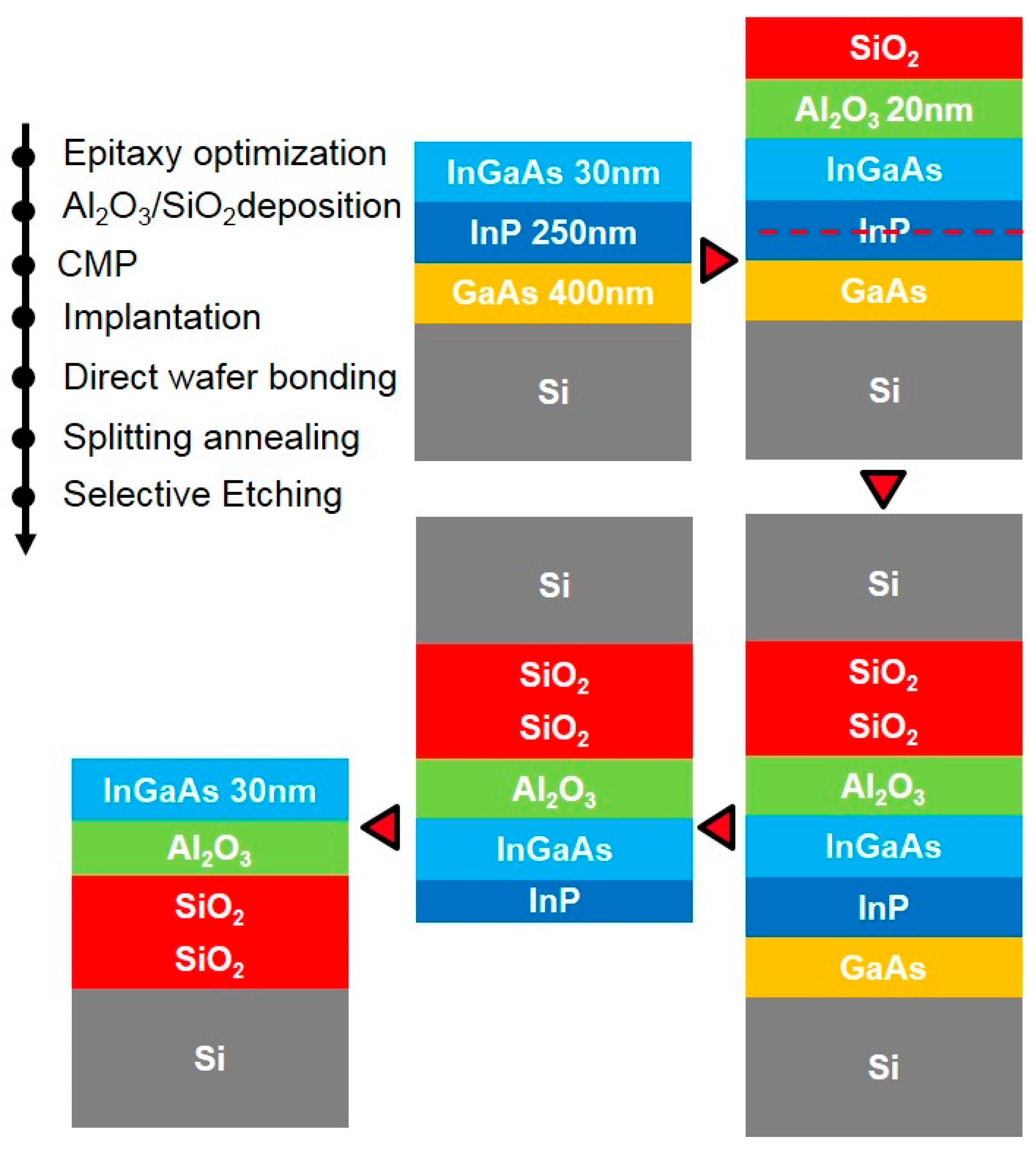
Figure 1 shows the process flow to fabricate InGaAs-OI substrates using Smart CutTM technology. A thin film (30 nm) is grown via metal organic chemical vapor deposition (MOCVD) on a 300-mm on-axis (100) Si substrate using an optimized InP/GaAs (250 nm/500 nm) metamorphic buffer to minimize the final surface roughness. An amorphous Al2O3 layer is deposited by atomic layer deposition (ALD) at 300 °C using tri-methyl-aluminum (TMA) and H2O as precursors. A SiO2 layer is then deposited on top of the Al2O3 to optimize the direct bonding parameters. The films are annealed between 300 °C to 600 °C in nitrogen gas for 1 h to stabilize the layers. The future buried oxide (BOX) thickness and surface roughness are controlled by a chemical-mechanical polishing step (CMP). The H+ implantation can be located in the metamorphic buffer (inside the InP layer in our case) or on the Si substrate. Then, the direct wafer bonding occurs on a thermally oxidized Si substrate. The splitting is performed via thermal annealing. The finishing step is done by chemical selective etching in the case of a splitting in the InP layer and CMP followed by chemical selective etching in the case of a splitting in the Si substrate. The final InGaAs thin film was characterized by AFM, HRXRD, and TEM.
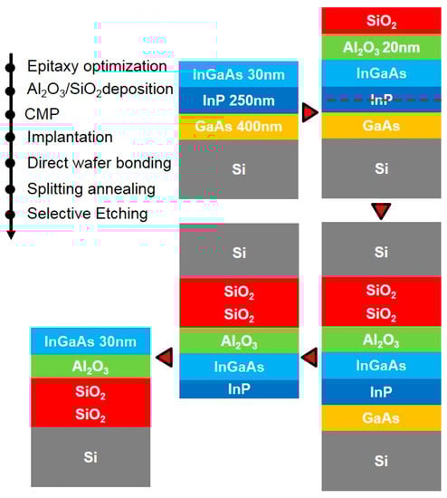
Figure 1.
The fabrication process flow of the InGaAs-OI substrates using Smart CutTM technology inside the InP buffer layer.
3. Results and Discussion
The III-V epitaxy growth process has been optimized to reduce the surface roughness values by a factor of two. This was possible thanks to an increase in the GaAs layer thickness. The obtained values (RMS = 1.91 nm, PV = 16 nm) were low considering the large lattice mismatch between Si and InGaAs (about 8%) and our thin total buffer thickness (665 nm) [5,6,7]. To achieve splitting in the InP layer, we increased the InP layer by up to 430 nm. The crystalline defects were localized in the GaAs layer, while low crystalline defects were observed in the thin InGaAs layer, as shown on TEM image in Figure 2.
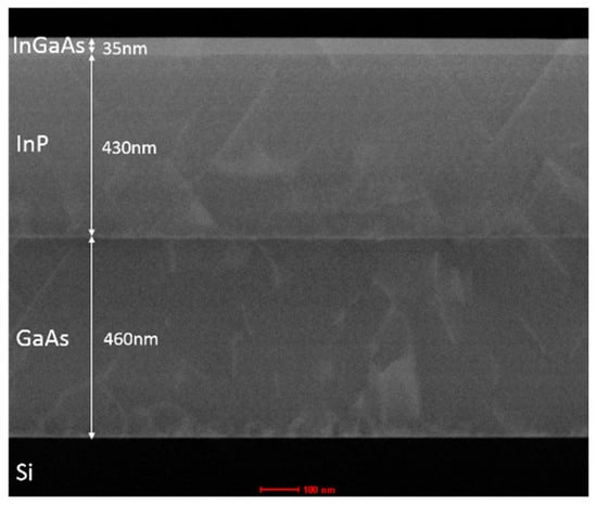
Figure 2.
TEM image <100> of the complete III-V epitaxial stack.
This optimization allows us to substantially reduce the thickness of the dielectric capping layer, which is used to reduce the surface roughness by using a well-known CMP process on this material. The study of the direct bonding interface quality was done in terms of annealing temperatures [8].
3.1. Bonding Condition Optimization
The bonding interface quality of different bonding configurations (Al2O3//Al2O3, Al2O3//Si, Al2O3//SiO2, and Al2O3 under SiO2//SiO2) were studied as a function of post bonding annealing. Silicon substrates were used for this study, and SAM images of the results have been presented in previous articles [5,6,7]. Al2O3 layers were pre-annealed at 600 °C in N2 ambient conditions and then cleaned in megasonic de-ionized water before bonding. SiO2 were prepared by polishing and hydrophilic cleaning. At room temperature (RT), no defects were observed after bonding for all stacks thanks to these efficient cleaning processes. All the bonding conditions present no defects up to 400 °C, except the Al2O3/Si bonding, which is already defective. At over 400 °C, only the last stack (with the SiO2//SiO2 bonding configuration) presented good performance in temperature without bonding defects up to 600 °C. This configuration avoids the diffusion of bonding interface water at the Al2O3//Si interfaces, which are known to be weak and easily defectives [8,9].
This deposited SiO2 layer is essential in the bonding process for two reasons: it can be easily polished to allow the DWB, and it allows the best bonding condition, but a pre-annealing before bonding (at 600 °C) is necessary to avoid defect at 600 °C after bonding [5].
This oxide layer thickness is driven by the initial III-V stack roughness and the implantation process conditions. This optimal bonding condition was applied to the InGaAs-OI process. We obtained direct bonding with no defects at room temperature, and the Smart CutTM technology was achieved either in the InP layer or on the Si substrate.
3.2. Fracture in the InP Buffer Layer
We investigated splitting conditions for the fracture to be located inside the epitaxial InP layer. For bulk InP, implantation temperature was identified as playing an important role [10]: some groups have reported that the temperature of an InP wafer during implantation should be kept below 0 °C [11,12], and others have claimed that heating the wafers during implantation is mandatory [12,13].
We performed H+ implantations in the InP epitaxial buffer layer at different temperatures using 300-mm Al2O3/InP/GaAs/Si wafers. In our case, we were able to obtain a fracture using “standard” temperature control during the implantation step, i.e., the wafers were maintained close to room temperature thanks to a backside gas cooling combined with water circulation in the chuck. The maximum of H+ implantation concentration were localized in the middle of the InP layer. Micro-cracks were observed in the InP layer after annealing at 300 °C, as seen on the SEM cross-section image [6]. These results indicate the layer transfer capability, which was confirmed during the InGaAs-OI fabrication.
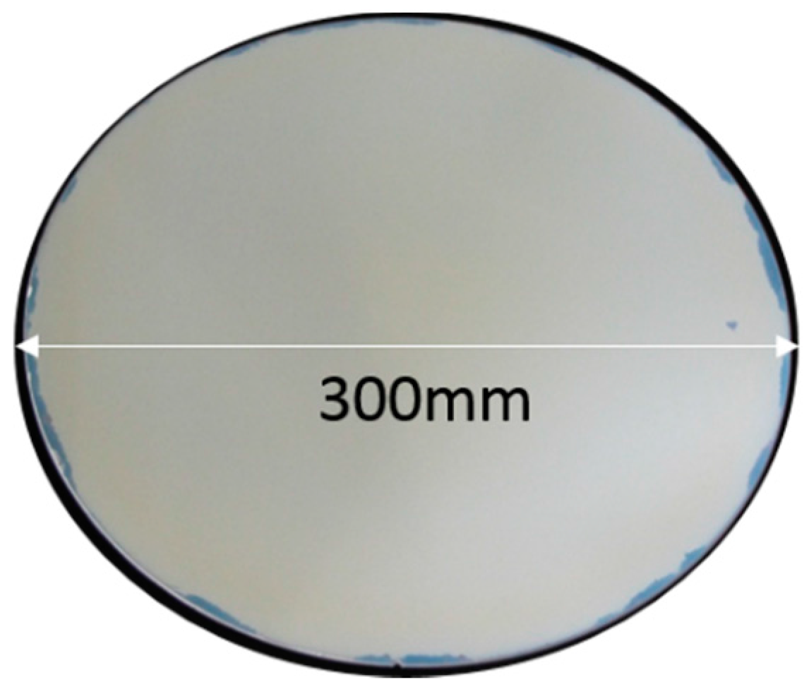
A picture of the 300-mm InGaAs-OI substrate with thin film transfer is shown on Figure 3. No crystal defects were observed. HRXRD measurements were performed both after splitting and the InP chemical selective etch. The full width at half maximum, the rocking curve of the InGaAs transferred was approximately 0.38°. Thus, the InGaAs layer remained crystalline during the overall process (2θ = 63.24°).
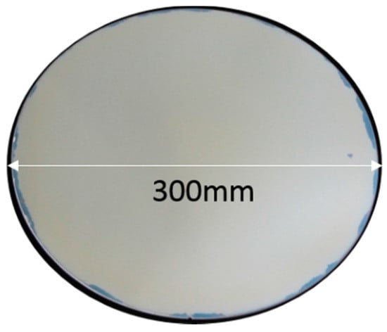
Figure 3.
Picture of a 300 mm InGaAs-OI substrate after transfer using Smart CutTM technology.
4. Conclusions
We here demonstrated 300 mm InGaAs-OI substrates with Smart CutTM technology. The transfer of a 30 nm-thick In0.53Ga0.47As layer grown on a 300 mm Si substrate by MOCVD shows good quality with a low defect density. Bonding interface quality was optimized in this work to maintain a defect-free bonding interface up to 600°C. Moreover, the process conditions were found to induce splitting in the InP epitaxial layer.
Acknowledgments
The authors acknowledge the financial support of the EU FP7 COMPOSE3 project, and IMEC for epitaxial donor wafers allowing the first transfer and SOITEC for the common laboratory program.
Author Contributions
T. Baron and M. Martin achieved the epitaxial substrate to optimize the InGaAs layer. G. Gaudin and IMEC donated epitaxial wafers allowing the first transfer. S. Favier, A. Salaun, P. Gergaud, and M. Cordeau contributed to characterization. M.C. Roure and P. Besson developed chemical selective etching. C. Morales, E. Beche, and F. Fournel performed the direct wafer bonding experiment. F. Mazen developed implantation condition process. C. Veytizou, L. Ecarnot, D. Delprat, I. Radu and T. Signamarcheix took part in discussion to the project. S. Sollier and J. Widiez conceived the process flow and wrote the paper. All authors have read and approved the final manuscript.
Conflicts of Interest
The authors declare no conflict of interest.
Abbreviations
The following abbreviations are used in this manuscript:
| MOSFET | metal oxide semiconductor field effect transistor |
| InGaAs-OI | indium–gallium–arsenic on an insulator |
| DWB | direct wafer bonding |
| SEM | scanning electron microscopy |
| SIMS | secondary ion mass spectrometry |
| TEM | transition electron microscopy |
| HR-XRD | high resolution X-ray diffraction |
| SAM | scanning acoustic microscopy |
References
- Pearsall, T.P.; Hirtz, J.P. The carrier mobilities in Ga0.43In0.57As grown by organo-metallic CVD and liquid-phase-epitaxy. J. Cryst. Growth 1981, 54, 127–131. [Google Scholar] [CrossRef]
- Ungersboeck, E.; Dhar, S.; Karlowatz, G.; Sverdlov, V.; Kosina, H.; Selberherr, S. Effect of general strain on the band structure and electron mobility of Si. IEEE Trans. Electron Devices 2007, 54, 2183–2190. [Google Scholar] [CrossRef]
- Lin, Y.-C.; Huang, M.-L.; Chen, C.-Y.; Chen, M.-K.; Lin, H.-T.; Tsai, P.-Y.; Lin, C.-H.; Chang, H.-C.; Lee, T.-L.; Lo, C.-C.; et al. Low interface trap density Al2O3/In0.53Ga0.47As MOS capacitor fabricated on MOCVD-grown InGaAs epitaxial layer on Si substrate. Appl. Phys. Express 2014, 7, 041202. [Google Scholar] [CrossRef]
- Widiez, J.; Hartmann, J.M.; Mazen, F.; Sollier, S.; Veytizou, C.; Bogumilowicz, Y.; Augendre, E.; Martin, M.; Gonzatti, F.; Roure, M.C.; et al. SOI-type Bonded Structures for Advanced Technology Nodes. ECS Trans. 2014, 64, 35–48. [Google Scholar] [CrossRef]
- Sollier, S.; Widiez, J.; Gaudin, G.; Mazen, F.; Baron, T.; Martin, M.; Roure, M.C.; Besson, P.; Morales, C.; Beche, E.; et al. 300 mm InGaAsOI substrate fabrication using the Smart CutTM technology. In Proceedings of the 2015 IEEE SOI-3D-Subthreshold Microelectronics Technology Unified Conference (S3S), Rohnert Park, CA, USA, 5–8 October 2015.
- Widiez, J.; Sollier, S.; Baron, T.; Martin, M.; Gaudin, G.; Mazen, F.; Madeira, F.; Favier, S.; Salaun, A.; Alcotte, R.; et al. First demonstration of 300 mm InGaAs-On-Insulator substrates fabricated using the Smart Cut™ technology. In Proceedings of the 2015 International Conference on Solid State Devices and Materials (SSDM), Sapporo, Japan, 27–30 September 2015.
- Widiez, J.; Sollier, S.; Baron, T.; Martin, M.; Gaudin, G.; Mazen, F.; Madeira, F.; Favier, S.; Salaun, A.; Alcotte, R.; et al. 300 mm InGaAs-on-insulator substrates fabricated using direct wafer bonding and the Smart Cut™ technology. Jpn. J. Appl. Phys. 2016, 55, 04EB10. [Google Scholar] [CrossRef]
- Beche, E.; Fournel, F.; Larrey, V.; Rieutord, F.; Morales, C.; Charvet, A.-M.; Madeira, F.; Audoit, G.; Fabbri, J.-M. Direct Bonding Mechanism of ALD-Al2O3 Thin Films. ECS J. Solid State Sci. Technol. 2015, 4, P171–P175. [Google Scholar] [CrossRef]
- Yokoyama, M.; Iida, R.; Ikku, Y.; Kim, S.; Takagi, H.; Yasuda, T.; Yamada, H.; Ichikawa, O.; Fukuhara, N.; Hata, M.; et al. Formation of III-V-on-insulator structures on Si by direct wafer bonding. Semicond. Sci. Technol. 2013, 28, 094009. [Google Scholar] [CrossRef]
- Singh, R.; Christiansen, S.H.; Moutanabbir, O.; Gösele, U. The Phenomenology of Ion Implantation-Induced Blistering and Thin-Layer Splitting in Compound Semiconductors. J. Electron. Mater. 2010, 39, 2177–2189. [Google Scholar] [CrossRef]
- Hayashi, S.; Bruno, D.; Goorsky, M.S. Temperature dependence of hydrogen-induced exfoliation of InP. Appl. Phys. Lett. 2004, 85. [Google Scholar] [CrossRef]
- Luce, F.P.; Reboh, S.; Vilain, E.; Madeira, F.; Barnes, J.P.; Rochat, N.; Salvetat, T.; Tauzin, A.; Milesi, F.; Mazen, F.; et al. Influence of implantation temperature on the formation of hydrogen-related defects in InP. In Proceedings of the 2014 20th International Conference on Ion Implantation Technology (IIT), Chico, CA, USA, 26 June–4 July 2014.
- Tong, Q.Y.; Gösele, U.M. Wafer Bonding and Layer Splitting for Microsystems. Adv. Mater. 1999, 11, 1409–1425. [Google Scholar] [CrossRef]

© 2016 by the authors; licensee MDPI, Basel, Switzerland. This article is an open access article distributed under the terms and conditions of the Creative Commons Attribution (CC-BY) license (http://creativecommons.org/licenses/by/4.0/).