Article

A Design and Theoretical Analysis of a 145 mV to 1.2 V Single-Ended Level Converter Circuit for Ultra-Low Power Low Voltage ICs †

1
The Charles L. Brown Department of Electrical and Computer Engineering, University of Virginia, Charlottesville, VA 22904, USA
2
Department of Computer Science, University of Virginia, Charlottesville, VA 22904, USA
3
PsiKick Inc., Charlottesville, VA 22902, USA
4
Department of System and Information Engineering, University of Virginia, Charlottesville, VA 22904, USA
*
Author to whom correspondence should be addressed.
This paper is an extended version of the paper: Y. Huang, A. Shrivastava and B. H. Calhoun, “A 145 mV to 1.2 V single ended level converter circuit for ultra-low power low voltage ICs,” SOI-3D-Subthreshold Microelectronics Technology Unified Conference (S3S), 2015 IEEE, Rohnert Park, CA, USA, 2015, pp. 1–3, doi:10.1109/S3S.2015.7333489.
J. Low Power Electron. Appl. 2016, 6(3), 11; https://doi.org/10.3390/jlpea6030011
Submission received: 31 March 2016 / Revised: 4 June 2016 / Accepted: 16 June 2016 / Published: 23 June 2016
(This article belongs to the Special Issue Selected Papers from IEEE S3S Conference 2015)

Abstract

:
This paper presents an ultra-low swing level converter with integrated charge pumps that shows measured conversion in a 130-nm CMOS test chip from an input at a 145-mV swing to a 1.2-V output. Lowering the input allowable for a single-ended level converter supports energy harvesting systems that need to use very low voltages.

1. Introduction

Energy autonomy is a critical feature required to enable the large-scale deployment of ultra-low power (ULP) systems in the Internet of things (IoT), with energy harvesting being accepted as a more viable means to provide power. Modern energy harvesting circuits can now harvest energy from input voltages as low as 10 mV [1]. However, many challenges face energy harvesting circuits, which require operation at very low power and voltage levels [2]. Figure 1 shows the block diagram of a generic energy harvesting system. The lifetime of the system depends on the energy stored on the energy harvesting capacitor C to provide power for the system. At runtime, as the energy stored on C is being consumed, the voltage on the capacitor, V C A P , is decreasing. The voltage at which the system stops operating (system threshold voltage) must be brought down to increase system lifetime. The minimum energy point has been proposed as the most optimal point to operate a system [3]. However, to maximize the utilization of stored energy on a capacitor, the system needs to operate from the lowest possible voltage. From the energy utilization perspective, the system threshold voltage should be brought down as low as possible to make full use of the stored energy. To more fully take advantage of the energy stored on the energy harvesting capacitor, SoCs (system on chip) under ultra-low voltage have been proposed in [4], which operate below 160 mV. Typical ULP (ultra low power) SoCs frequently use timers to keep the circuit functional, even when the voltage is very low [5]. However, the outputs of these ULP subthreshold circuits also operate at a very low voltage level, which causes communication problems with the core voltage levels off-chip or with other peripheral circuits. Level converters are necessary in such a system to interface between the low voltage domain and the nominal voltage domain. In this paper, we present a low swing level converter that can convert from the 100-mV (simulation) and 145-mV (measurement) level input signals to 1.2 V using a single-ended charge pump-based topology.
A traditional level converter can convert from nearly 400 mV to 1.2 V via a cross-coupled stage. However, in a low power system, the system life time can be extended by lowering the operation voltage, the same with the energy consumption. Lower input signals can kill the positive feedback and prevent conversion with the traditional design. Several low voltage level converter circuits have been proposed in the literature. A low swing level converter can convert from a range of 210 mV to 950 mV to 1.2 V with a bootstrapping technique [7]. A dynamic logic level converter can convert 300 mV to 2.5 V, which is employed with a clock synchronizer [8]. However, being a dynamic circuit, it can only operate at higher frequencies and uses higher power and area. A single-ended interconnect circuit achieves level conversion from 300 mV [9], but it is dynamic and higher power. In [10], a current mirror structure is proposed, which allows the conversion from 200 mV across technologies. A two-stage ULP level converter can convert from 188 mV to 1.2 V achieving ULP operation [11]. In this work, we present two design constraints for the main stream cross-coupled level converter. Furthermore, we propose a level converter that can potentially convert 100 mV to 1.2 V using a charge pump. The charge pump stage increases the swing before level conversion, which helps in initiating the positive feedback. Our measurement results show conversion from 145 mV to 1.2 V.
This paper is organized as follows: In Section 2, we discuss two main categories of conversion techniques for level converter design: amplification-based conversion and boosted swing-based conversion. In this section, we analyze the level conversion techniques in detail and give two design constraints of an amplification-based subthreshold level converter, which is the mainstream. In Section 3, we propose our own work integrating the two techniques introduced in Section 2. We first introduce our design architecture and two different designs based on this architecture. We then show the simulation results of the proposed work. In Section 4, we show the chip fabricated using 130-nm CMOS technology and the measurement results of the proposed designs. Lastly, we compare our work with the state-of-the-art in Section 5.

2. Level Conversion Techniques

In this chapter, we discuss the state-of-the-art level conversion techniques in the subthreshold domain. We introduce the level conversion techniques in two categories based on their different fundamental structure and working mechanisms: amplification-based and boosted swing-based level conversions. Specifically, we discuss in detail the theoretical analysis of the amplification-based level conversion.

2.1. Amplification-Based Level Conversion

The first main type of level converter design is based on an amplification mechanism that aims to enhance the pull down network. We will analyze this type of design in this subsection.

2.1.1. Designs of Amplification-Based Level Converters

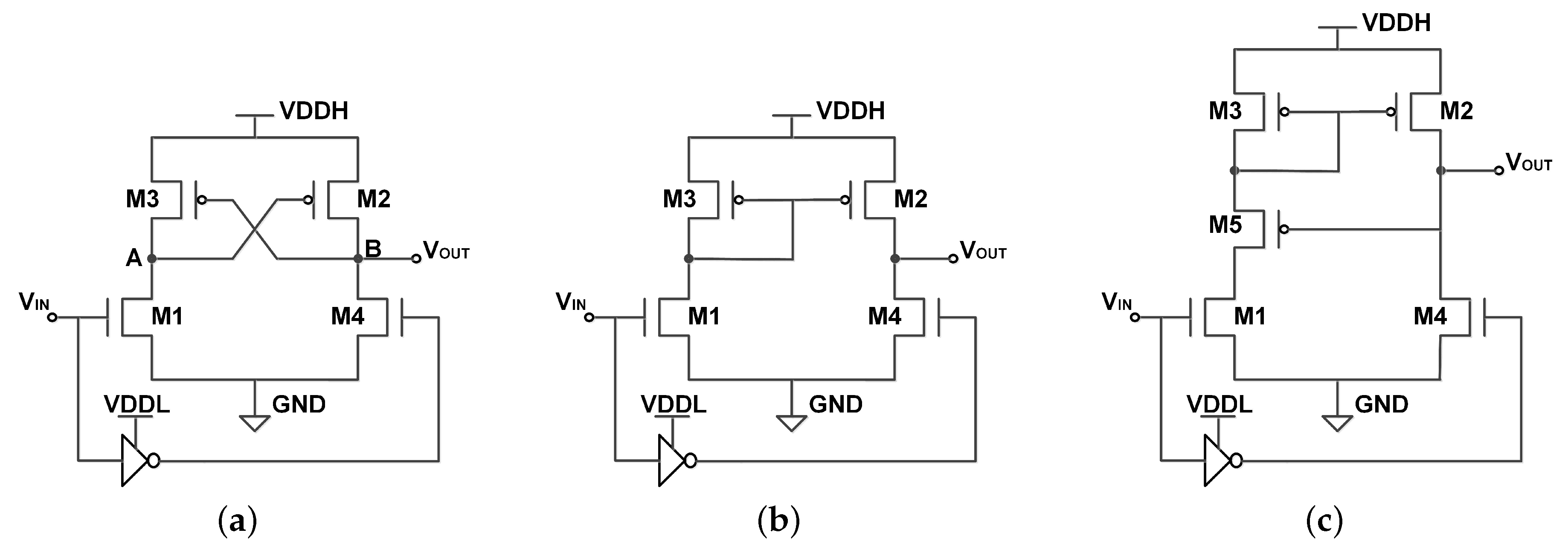
Figure 2a,b shows two of the most traditional amplification-based level converter topologies [12]. Following the naming convention in [10], the level converter shown in Figure 2a is the conventional cross-coupled level converter (CCLC), and the level converter shown in Figure 2b is the current mirror-based level converter (CMLC). CCLC is a full-swing design, which can pull up the input low voltage VDDL up to the high voltage rail VDDH by taking advantage of positive feedback. However, also due to the positive feedback, the conversion capability decreases, because it has to meet the ratio constraint between the pull up network and pull down network. CMLC uses a basic current mirror. CMLC has a stronger conversion capability due to the level shift using the differential amplifier action. However, CMLC cannot eliminate the direct current when input is high, which leads to a higher static power consumption.
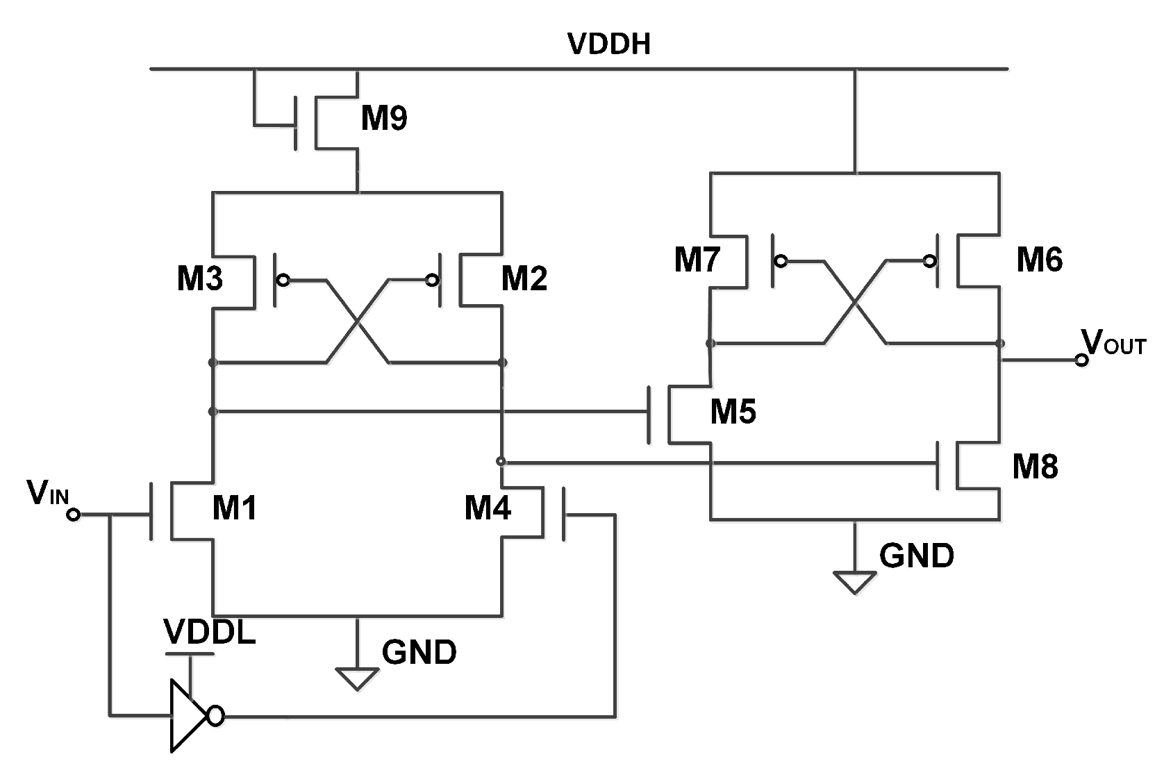
Figure 2c is a design with an Wilson current mirror (WCMLC) [13]. As discussed in the paper and [10], WCMLC is robust, but is not repeatable for the Monte Carlo sizing optimization across different technologies. In [14], they used a three-stage design based on the topology in Figure 2a, which is able to convert from 200 mV to 1.2 V. This cascaded design requires three supply voltages and size adjustment for each of the three intermediate conversion stages, which increases the design and power management complexity. Based on this work in [14], the authors in [11] proposed a two-stage cross-coupled level converter as in Figure 3. They added an NMOS header in the first stage to weaken the pull up network (PUN) to enhance the conversion of the shifter. This simplified the design of [14] and achieves the conversion from 188 mV in the subthreshold. In this paper, we will note this design as a two-stage CCLC (TSCCLC), as in [10].

2.1.2. Theoretical Analysis of Amplification-Based Level Converters

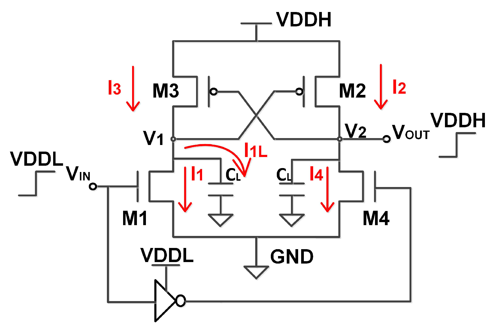
We will discuss two design constraints here using the example of CCLC: the sufficient conversion condition and balanced switching condition. We will prove that the latter gives a stronger design constraint. We will perform all of the analysis based on the notation in Figure 4. Finally, we discuss the drawbacks of CMLC.

Sufficient Conversion Condition for CCLC

The essential point of a subthreshold amplification-based level converter design is to adjust the ratio of the pull up network and pull down network, so that the pull down network is strong enough to achieve the conversion when the input is ‘high’ in the subthreshold. As in CCLC, we perform a specific analysis of the design constraints for a sufficient conversion in the subthreshold, as marked in Figure 4.
In the analysis, we use V t n and V t p to represent the threshold voltage for NMOS and PMOS, respectively. k n and k p are the gain factor of NMOS and PMOS, while k s n and k s p are for the subthreshold. When input switches from ‘low’ to ‘high’, at this moment, V 1 is V D D H , so M 1 works in saturation region:
I 1 = k n ( V g s - V t n ) 2 = k n ( V D D L - V t n ) 2
I 3 works in linear region:
I 3 = k p ( ( V D D H - V 2 - V t p ) ( V D D H - V 1 ) - ( V D D H - V 1 ) 2 )
M 2 and M 4 are off, so we get I 2 and I 4 :
I 2 = I D P 0 W L e q V g s n k T = k s p e q ( V D D H - V 1 ) n k T
I 4 = I D N 0 W L e k B q V g s n k T = k s n
For a successful conversion, when input switches from ‘low’ to ‘high’, the pull up network should be able to overcome the pull down network at node V 2 to break the internal equilibrium and trigger the positive feedback:
I 2 I 4
Represent I 2 and I 4 by Equations (3) and (4):
k s p e q ( V D D H - V 1 ) n k T k s n
Thus, for the minimum scenario:
q V D D H - V 1 n k T = ln k s n k s p
Then, we get:
V D D H - V 1 = n k T q ln k s n k s p
Assuming that in subthreshold region, the leakage very slowly charges C L (on the right part of CCLC), V 2 will not rise fast and stays close to zero, and V 1 will stay close to V D D H .
Thus, in Equation (2), let V 2 = 0 :
I 3 = k p ( V D D H - V t p ) ( V D D H - V 1 )
The sufficient condition for a successful conversion is to break the equilibrium between the pull up network and pull down network and be able to pull down V 1 :
I 1 I 3
Take Equations (1) and (9). Thus:
k n ( V D D L - V t n ) 2 k p ( V D D H - V t p ) ( V D D H - V 1 )
Then, take Equation (8) into Equation (11), we get the final sufficient condition for a conversion:
k n k p V D D H - V t p ( V D D L - V t n ) 2 n k T q ln k s n k s p
Equation (12) shows that NMOS and PMOS cannot be arbitrarily sized to get the desired ratio for k n and k p , because the sizing of NMOS and PMOS also determines the ratio of k s n and k s p at the same time. Therefore, the cross-coupled level converter (CCLC) cannot be used reliably for subthreshold operations, as the subthreshold leakage plays a part in triggering the positive feedback.

Balanced Switching Condition for CCLC

In a level converter design, to get a balance of rising and falling time (i.e., t L H = t H L ), we must consider the following constraint:
I 2 = C L d V 2 d t
Additionally, at the same time, I 2 is:
I 2 = k p ( V D D H - V 1 - V t p ) 2
Thus, we get:
C L d V 2 d t = k p ( V D D H - V 1 - V t p ) 2
Similarly for I 1 L , we have:
I 1 L = k n ( V D D L - V t n ) 2 - k p ( V D D H - V 1 - V t p ) 2
Additionally:
I 1 L = C L d V 1 d t
Therefore, we get:
C L d V 1 d t = k n ( V D D L - V t n ) 2 - k p ( V D D H - V 1 - V t p ) 2
Let d t = d t using Equations (15) and (18):
[ k n ( V D D L - V t n ) 2 - k p ( V D D H - V 1 - V t p ) 2 ] d V 2 = k p ( V D D H - V 1 - V t p ) 2 d V 1
In a balance design where t L H = t H L , when V 1 changes from zero to V D D H , V 2 changes from V D D H to zero. Take this into Equation (19):
V D D H 0 [ k n ( V D D L - V t n ) 2 - k p ( V D D H - V 2 - V t p ) 2 ] d V 2 = 0 V D D H k p ( V D D H - V 1 - V t p ) 2 d V 1
Solve Equation (20); we get the design constraint for a subthreshold balanced level converter:
k n k p = 2 V D D H ( V D D H - V t p ) ( V D D L - V t n ) 2
The balance design constraint Equation (21) is a much stronger bound than the sufficient conversion constraint Equation (12). In other words, it is more difficult to make a subthreshold level converter with an equal rising and falling time. The bound of Equation (12) gives a design constraint of a successful conversion, but cannot guarantee the balance of switching performance.

Drawback of CMLC

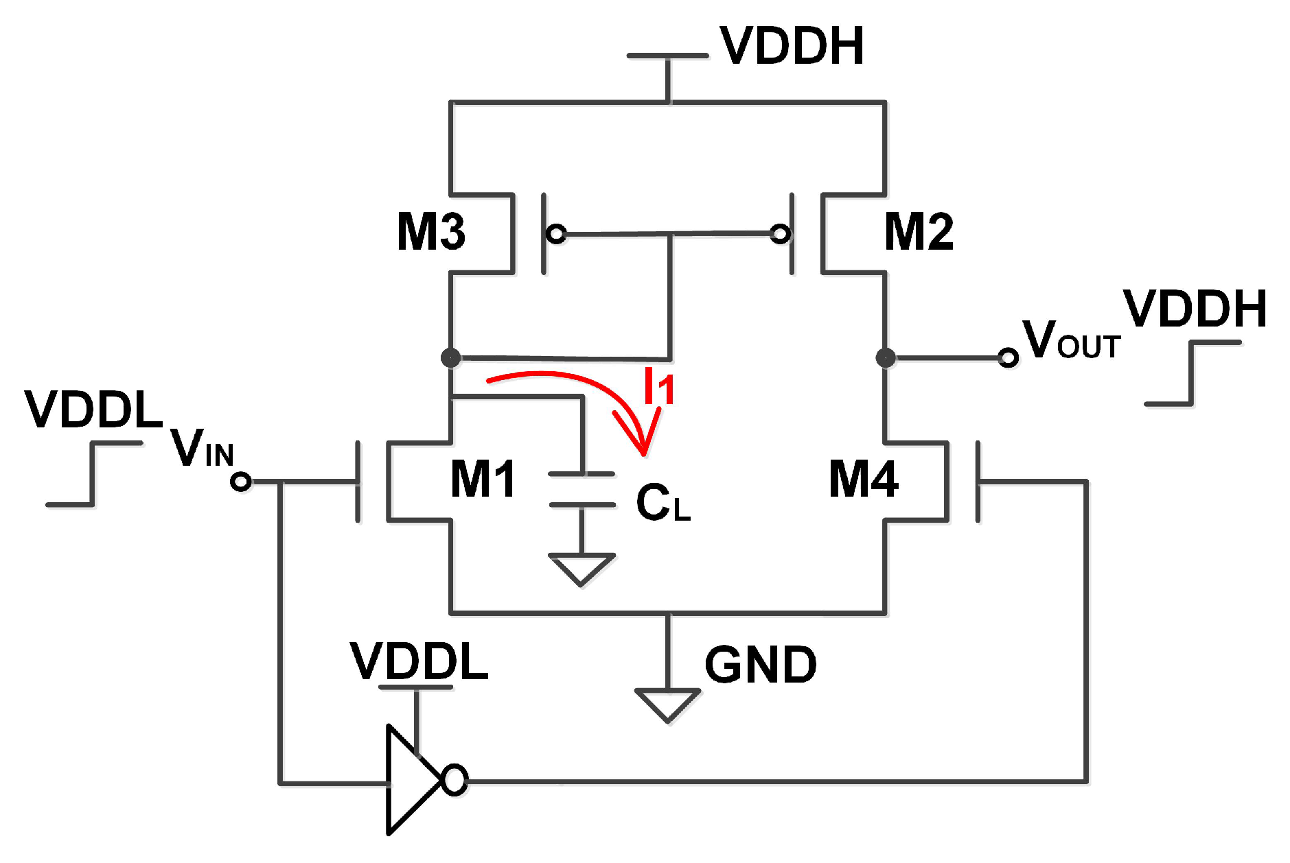
In the current mirror design (CMLC), the biggest problem is the direct current and the slow conversion in the subthreshold. We will do a simple analysis using Figure 5.
When input is ‘high’ ( V D D L ), M 1 works in the saturation region:
I 1 = k n ( V g s - V t n ) 2 = k n ( V D D L - V t n ) 2
However, in the subthreshold, the case in Equation (22) will be:
I 1 = k s n e q V D D L n k T
With the existence of the current mirror, we also have:
I 1 = C V D D H T r i s e
Combine Equations (23) and (24):
T r i s e = C L V D D H k s n 1 e q V D D L n k T
From Equation (25), a current mirror level converter has a very slow conversion in the subthreshold (low VDDL). This is the biggest bottleneck of this kind of design.

2.2. Boosted Swing-Based Level Conversion

The other type of level converter is the boosted swing-based level converter. Different with amplification-based level converters, boosted swing-based conversions happen by pulling the ‘high’ input signal higher first through boosting techniques. This is usually achieved by taking advantage of the characteristics of a capacitor.

Designs of Boosted Swing-Based Level Converters

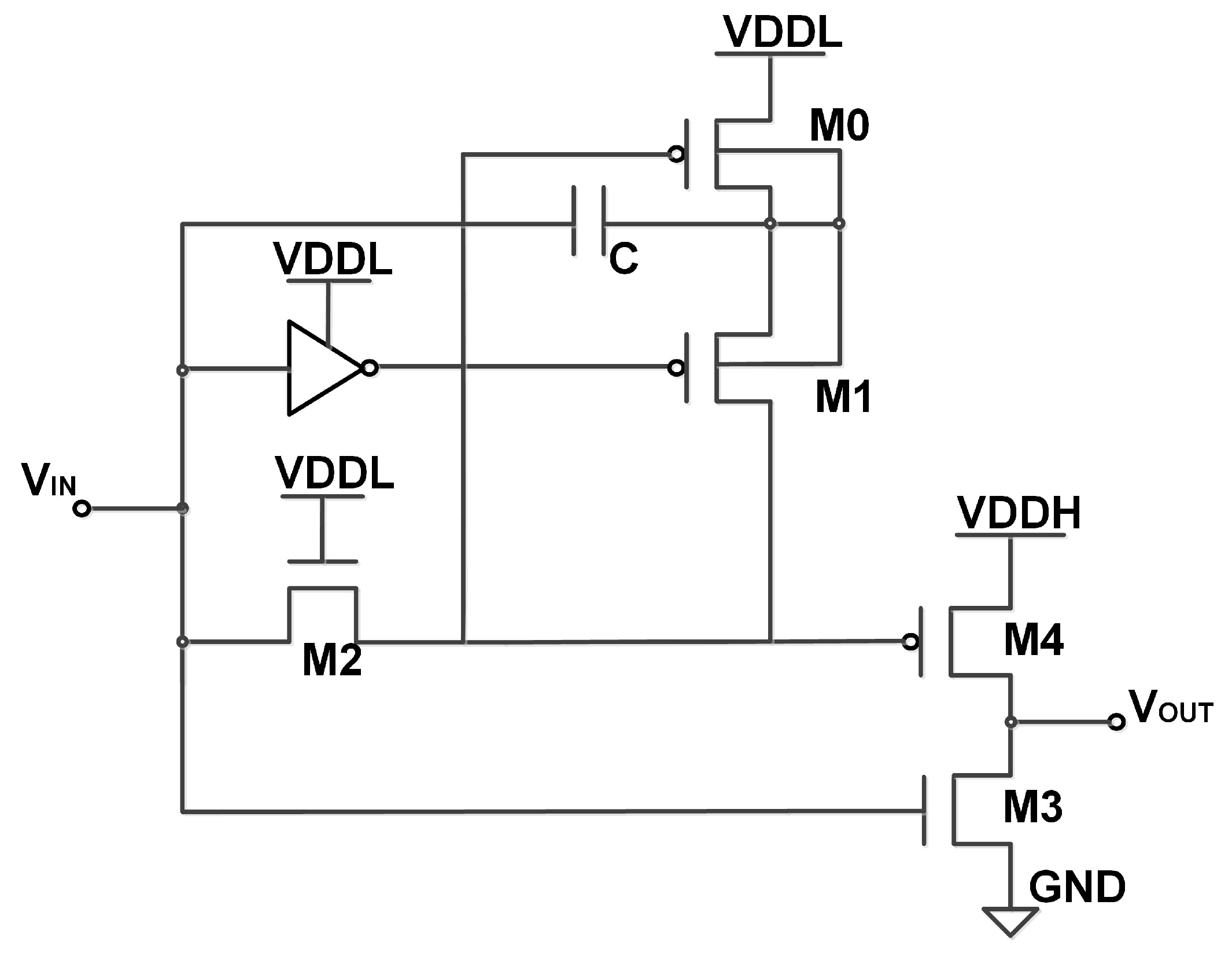
Figure 6 is a design based on the bootstrapping effect as reported in [15], lrc-converter as called in [7]. The drivers are enhanced by the bootstrapping techniques through the capacitor Cb. In a boosted swing-based level converter like Figure 6, when the input is low, the output is pulled up to VDDH by M 4 . The left plate of C b is ‘0’, and the right plate is pulled up to VDDL by M 0 . When the input is high (VDDL), M 2 passes a ‘0’ to M 0 ’s gate and turns it on, while M 1 is turned on at the same time. In this phase, the left plate of C b is pulled up from zero to VDDL (in the previous phase), and the right plate is pulled up from VDDL to 2× VDDL. The boosted 2× VDDL is passed to the gate of M 4 . In order to pull down the output to zero, it has to meet this condition to turn off M 4 completely:
  V D D L > V D D H
If this condition is not met, it will result in static current through M 4 . This design requires two power supplies, VDDH and VDDL, which increases the design complexity. In conclusion, the major problem of this level converter design is that it is dynamic and only works at high frequency. For example in Figure 6, the gate of M 4 will slowly decrease to V D D L at a lower frequency of signals, which causes high static current.
The proposed work in [7] is based on the same bootstrapping effects and reduced the circuit complexity with an improvement of power and delay. A similar design is proposed in [9]. The boosted swing-based design is usually preferred in the interconnect design to work with reducing the power consumption or re-boost the signals to communicate with the core chip.

3. Proposed Low Voltage Level Converter

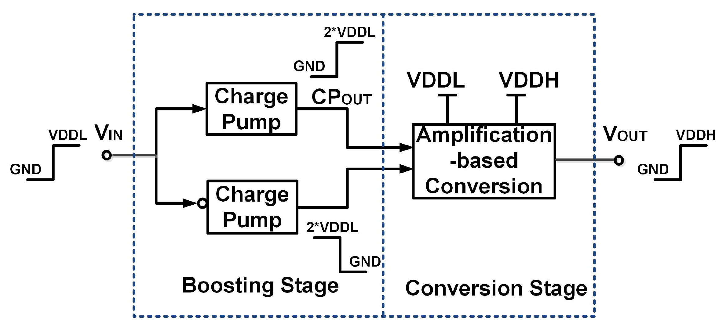
In this section, we introduce our proposed low power subthreshold single-ended level converter. Our design is based on both the amplification-based and boosted swing-based conversion techniques. The combination of the two design types of level converters achieves a stronger conversion capability that allows a deeper application in subthreshold ICs. This proposed design uses a two-staged architecture: boosting stage and conversion stage. The boosting stage is implemented with a subthreshold charge pump design, while the conversion stage uses the amplification-based techniques.
First, we propose the boosting part: a subthreshold charge pump. Next, we introduce our uniform design architecture, which takes advantage of this subthreshold charge pump. According to the architecture, we introduce two level converter designs and show the simulation results accordingly.

3.1. Subthreshold Charge Pump

Figure 7 shows the schematic of a 2× charge pump used in the proposed work and its sizing. When V I N is low, M 1 turns on, which turns on M 3 . X is pulled up to VDDL, while B is pulled down to GND by the inverter connected to it. Next, V I N goes high and turns on M2 and M5, which leads to the up-conversion of B from zero to VDDL. Since X was charged to VDDL previously, the up-conversion of B causes X to go from VDDL to 2× VDDL at the output of the charge pump. In this design, M 4 works as a capacitor to implement the boosting.
In deep subthreshold operation with a VDD between 100 mV and 300 mV, node X falls ideally at 200 mV and 600 mV, respectively. However, in the subthreshold, the low slew rate prevents a full doubling of voltage when VDD is very low (<200 mV) because of the higher discharge caused by leakage. Thus, we enhanced the pull down network. In this charge pump design, we do not require an additional body bias control circuit.

3.2. Implementation of the Proposed Level Converter

We propose two designs that use charge pump outputs to drive a traditional level converter CCLC, as in Figure 2a, and the improved two-stage amplification-based level converter from [11], as in Figure 3, respectively. We call the former proposed level converter the charge pump boosted level converter (CPBLC) in the rest of the paper, and we call the latter proposed level converter the charge pump boosted ultra-low swing level converter (CPBULS). Following the same naming convention, we use ULS to represent TSCCLC in the following comparison to simplify the relationship between different structures.

Uniform Architecture

Figure 8 shows the architecture of the proposed topology, which combines two charge pumps and a level converter design. The first stage provides the differential inputs doubled by the 2× charge pumps. The second stage is a cross-coupled differential inverter (e.g., the level converter designs in Figure 2) that restores the final output to full swing (zero to VDDH). The output of the charge pump stage overpowers the equilibrium of the second stage and drives the PMOS to pull up the internal node (e.g., A or B in Figure 2a and triggers the positive feedback within the conversion stage).

3.3. CPBLC and CPBULS

Deriving from the same proposed architecture, we use the boosting power of the subthreshold charge pump to trigger the conversion. We will omit the schematic of CPBLC and CPBULS, since their second stages have the same structure of CCLC as in Figure 2a and TSCCLC as in Figure 3.

Simulations

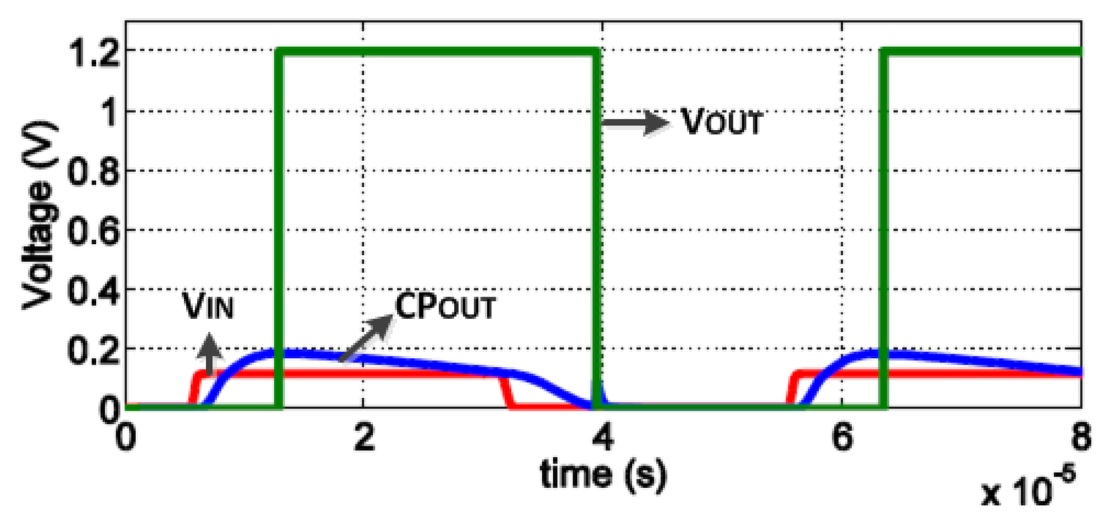
In Figure 9, it shows the functional waveform of CPBULS from the simulation of a VDDL of 120 mV. In fact, CPBLC works in a similar way. The signals labeled in Figure 9 correspond to the signals in Figure 8. As V I N goes high or goes low, one of the charge pump outputs, e.g., C P O U T , increases and thus initiates the positive feedback in the conversion stage, resulting in the amplification-based voltage conversion. From observation, when V I N just reaches its highest value (120 mV), the conversion cannot be successfully triggered. Instead, the boosting stage takes in V I N and pulls it up to 200 mV from 120 mV, as shown as C P O U T . When C P O U T is boosted to around 200 mV, the voltage conversion of the second stage successfully happens. This is as explained in Section 2: the boosted C P O U T successfully satisfies the sufficient conversion constraint in Equation (12). In other words, the boosting stage lowers the constraint of a sufficient conversion for the same amplification-based level converter design. Furthermore, in Figure 9, we can see that C P O U T will slowly decrease to V D D L , as well, like the design in Figure 6. However, the difference is, in our design, this will not cause static current.
Figure 10 shows the minimum input swing results of 100 Monte Carlo simulations for CPBULS, CPBLC and ULS level converters. The charge pump technique decreases the minimum operating voltage of [11] (TSCCLC), further lowered down to an average of 128 mV, while the best case (among the 100 iterations) is 99.6 mV in CPBULS and an average of 171 mV in CPBLC.
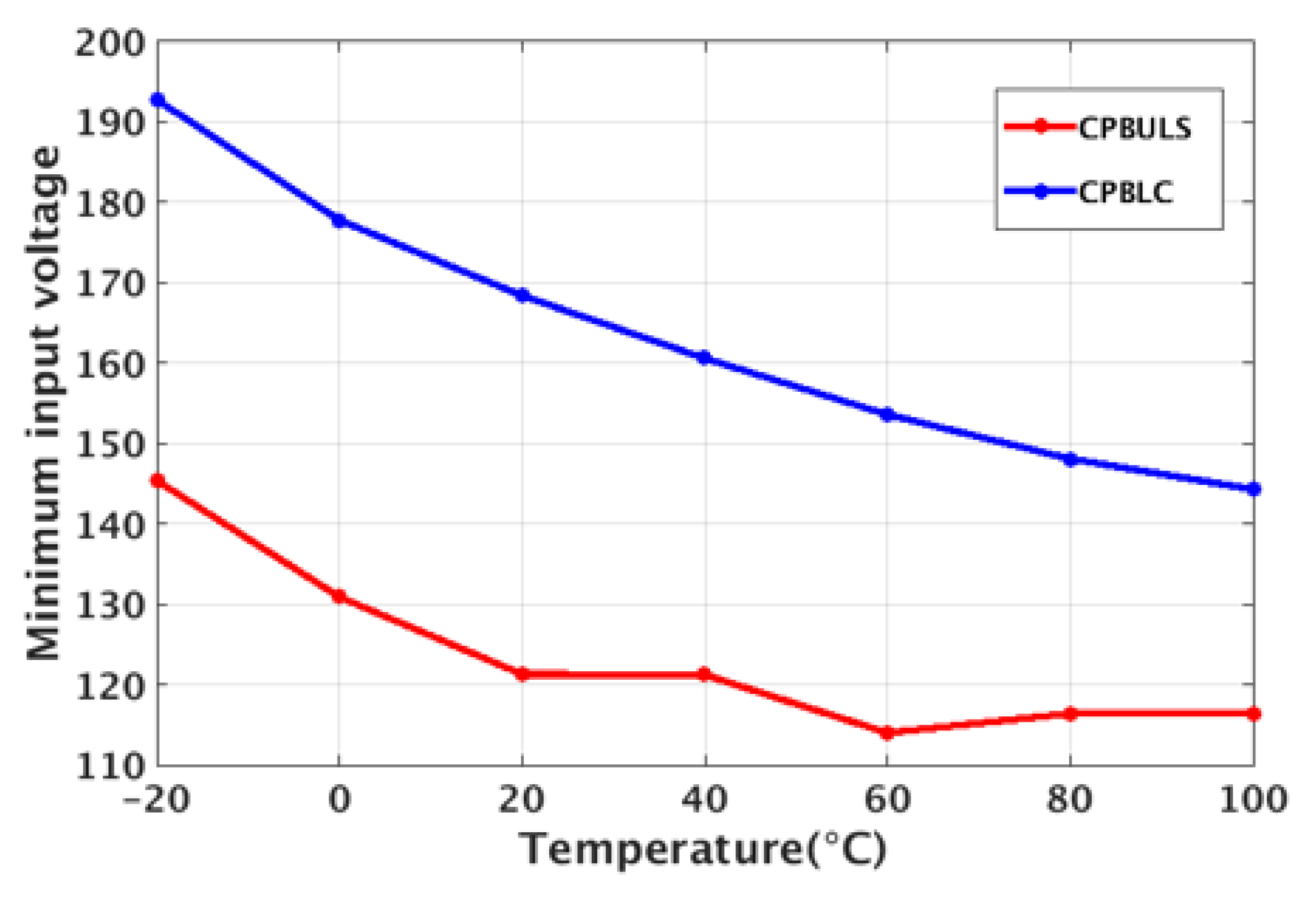
Figure 11 shows the simulation results of the minimum input voltage of CPBULS (red) and CPBLC (blue) level converters under different temperatures. At - 20 C, CPBULS and CPBLC can work at 145.4 mV and 192.8 mV respectively, while at 100 C, they can work at 116.4 mV and 144.3 mV, respectively. Simulation shows that our charge pump-based level converter has lower temperature dependence for the minimum operating voltage.
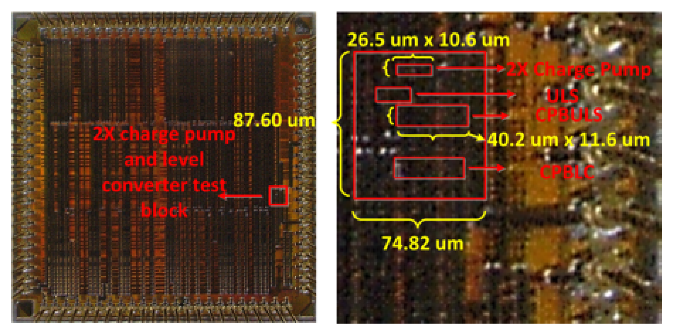
The proposed design was fabricated in a 130-nm CMOS process. Figure 12 shows the die photo of the test chip. The subthreshold charge pump takes 280 μm2, while CPBLC and CPBULS take around 466 μm2 with an unoptimized layout design and necessary peripheral circuits.

4. Measurements

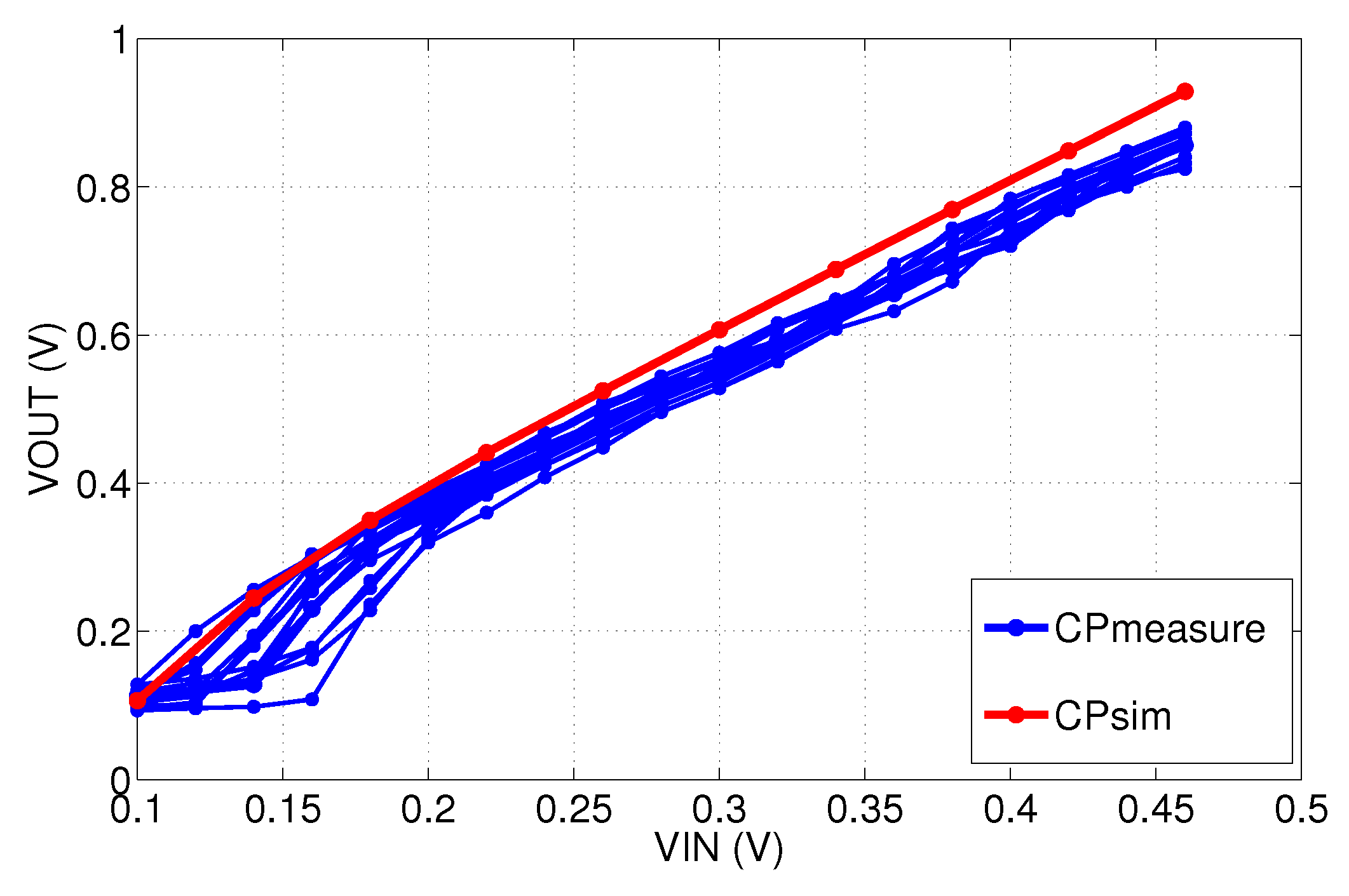
Figure 13 shows the measurements of the 2× charge pump from 15 chips, which starts working from a 170-mV input in the worst case. We show the simulation result together with the measurement results: the blue lines are the measurement results, while the red line is from simulation. After V I N is higher than 200 mV, the boosting factor is stable at 2×.
Figure 14 shows the measurement results of the minimum operational input swing for CPBULS, CPBLC and ULS level converters across the 15 chips. The CPBULS can achieve a mean minimum input voltage of 157 mV, while the CPBLC achieves the same at 198 mV. The CPBULS can reach a lowest input voltage of 145 mV. The limitation of this design is slower transition times that lead to higher energy per conversion due to the extra leakage.
Figure 15 shows the energy-delay measurement of CPBLC and CPBULS across 15 fabricated chips. The measurements were taken at three points: 200 mV, 300 mV and 500 mV. CPBLC and CPBULS can operate with a frequency of 35.6 kHz (28 us) and 50.1 kHz (19.96 us), respectively, at 200 mV for the best case, with a mean value of 12.8 kHz and 22.0 kHz, respectively. The best operation frequency is 66.9 kHz and 136.6 kHz at 300 mV, 109.7 kHz and 139.4 kHz at 500 mV, for CPBLC and CPBULS, respectively. As the operation voltage increases, the delay decreases, which is expected in an energy harvesting system where the worst case is when the operation voltage is the lowest. In the subthreshold energy harvesting system, there is much voltage variation. The proposed work is designed for an unregulated power supply, which can still successfully work in the worst cases (also known as when the operation voltage goes very low). From the measurement results of the 15 chips we fabricated, the best EDP value is 0.0015 pJ·ms for CPBLC and 0.0006 pJ·ms for CPBULS.
Another source of variation, the process, can also affect the behavior of this design. As in Figure 7, in the subthreshold, the low slew rate results in that node X cannot be charged to 2× VDDL due to the discharge caused by leakage. Thus, in the slow-fast corner, the discharge will further affect the boosting of X; and vice versa, in the fast-slow corner, the discharge is weakened; thus, the boosting is enhanced. For the same reason, as in Figure 7, we enhanced the pull down network.

5. Conclusions

This proposed level converter design is based on a subthreshold charge pump design, as shown in Figure 7. Due to the charge and discharge time of M 4 , the capacitor, its performance is not as good as conventional level converters at their operating voltages (300 to 400 mV). However, this design is a better choice for an ultra-low power energy harvesting system where performance is not the first priority, but the ability of using stored energy is instead, as discussed in Section 1. Thus, we try to make more use of the energy collected in the capacitor in Figure 1. The challenge is, the lower the level converter can operate at, the more energy the system can use to obtain a longer lifetime.
Table 1 compares prior work, both simulations and chip measurements. This proposed charge pump-based level converter CPBULS up-converts reliably from 145 mV to 1.2 V, which is a wider conversion range. The best energy per conversion is reported as 10 fJ in [10] from simulation results with a 90-nm technology. This work has a relatively lower maximum operating frequency with the lowest input swing, but achieves 1.2 pJ energy per conversion, which is 30% less than that in [8] from chip measurement and a 2× conversion ability. This proposed work can further improve the energy utilization of an ultra-low power system, such as an energy harvesting system.

Acknowledgments

We thank Kevin Leach for his help improving the writing of the paper, providing figures and giving his valuable suggestions.

Author Contributions

Yu Huang was responsible for authoring this paper, as well as the design and test of the circuits described here. Aatmesh Shrivastava helped with the theoretical analysis and the design of the circuit. Aatmesh Shrivastava and Benton H. Calhoun helped to guide this research, review the proposed circuits and edit this paper. Laura E. Barnes reviewed this paper.

Conflicts of Interest

The authors declare no conflict of interest.

Abbreviations

The following abbreviations are used in this manuscript:
ULP
Ultra low power
IoT
Internet of things
SoC
System on chip
CCLC
Cross-coupled level converter
CMLC
Current mirror-based level converter
WCMLC
Wilson current mirror level converter
PUN
Pull up network
PDN
Pull down network
TSCCLC/ULS
Two-stage cross-coupled level converter
CPBLC
Charge pump boosted level converter
CPBULS
Charge pump boosted ultra-low swing level converter

References

  1. Shrivastava, A.; Wentzloff, D.; Calhoun, B.H. A 10 mV-input boost converter with inductor peak current control and zero detection for thermoelectric energy harvesting. In Proceedings of the 2014 IEEE Custom Integrated Circuits Conference (CICC), San Jose, CA, USA, 15–17 September 2014; pp. 1–4.
  2. Klinefelter, A.; Roberts, N.E.; Shakhsheer, Y.; Gonzalez, P.; Shrivastava, A.; Roy, A.; Craig, K.; Faisal, M.; Boley, J.; Oh, S.; et al. 21.3 A 6.45 μW self-powered IoT SoC with integrated energy-harvesting power management and ULP asymmetric radios. In Proceedings of the 2015 IEEE International Solid-State Circuits Conference (ISSCC), San Francisco, CA, USA, 22–26 February 2015; pp. 1–3.
  3. Calhoun, B.H.; Chandrakasan, A. Characterizing and modeling minimum energy operation for subthreshold circuits. In Proceedings of the 2004 International Symposium on Low Power Electronics and Design (ISLPED’04), Newport Beach, CA, USA, 9–11 August 2004; pp. 90–95.
  4. Kulkarni, J.P.; Kim, K.; Roy, K. A 160 mV, fully differential, robust schmitt trigger based sub-threshold SRAM. In Proceedings of the 2007 International Symposium on Low Power Electronics and Design, Portland, OR, USA, 27–29 August 2007; pp. 171–176.
  5. Shrivastava, A.; Kamakshi, D.A.; Calhoun, B.H. A 1.5 nW, 32.768 kHz XTAL Oscillator Operational from a 0.3 V Supply. IEEE J. Solid-State Circuits 2016, 51, 686–696. [Google Scholar]
  6. Huang, Y.; Shrivastava, A.; Calhoun, B.H. A 145 mV to 1.2 V single ended level converter circuit for ultra-low power low voltage ICs. In Proceedings of the 2015 IEEE SOI-3D-Subthreshold Microelectronics Technology Unified Conference (S3S), Burlingame, CA, USA, 10–13 October 2015; pp. 1–3.
  7. García, J.C.; Nelson, J.A.M.; Nooshabadi, S. High performance bootstrapped CMOS low to high-swing level-converter for on-chip interconnects. In Proceedings of the 18th European Conference on Circuit Theory and Design (ECCTD 2007), Sevilla, Spain, 26–30 August 2007; pp. 795–798. [CrossRef]
  8. Chang, I.J.; Kim, J.j.; Kim, K.; Roy, K. Robust level converter for sub-threshold/super-threshold operation: 100 mV to 2.5 v. IEEE Trans. Very Large Scale Integr. (VLSI) Syst. 2011, 19, 1429–1437. [Google Scholar] [CrossRef]
  9. Shrivastava, A.; Lach, J.; Calhoun, B. A charge pump based receiver circuit for voltage scaled interconnect. In Proceedings of the 2012 ACM/IEEE International Symposium on Low Power Electronics and Design, Redondo Beach, CA, USA, 30 July–1 August 2012; pp. 327–332.
  10. Luo, S.C.; Huang, C.R.; Chiou, L.Y. Minimum convertible voltage analysis for ratioless and robust subthreshold level conversion. In Proceedings of the 2012 IEEE International Symposium on IEEE Circuits and Systems (ISCAS), Seoul, South Korea, 20–23 May 2012; pp. 2553–2556.
  11. Wooters, S.N.; Calhoun, B.H.; Blalock, T.N. An energy-efficient subthreshold level converter in 130-nm CMOS. IEEE Trans. Circuits Syst. II: Express Briefs 2010, 57, 290–294. [Google Scholar] [CrossRef]
  12. Koo, K.H.; Seo, J.H.; Ko, M.L.; Kim, J.W. A new level-up shifter for high speed and wide range interface in ultra deep sub-micron. In Proceedings of the IEEE International Symposium on IEEE Circuits and Systems (ISCAS 2005), 23–26 May 2005; pp. 1063–1065.
  13. Lütkemeier, S.; Rückert, U. A subthreshold to above-threshold level shifter comprising a wilson current mirror. IEEE Trans. Circuits Syst. II: Express Briefs 2010, 57, 721–724. [Google Scholar] [CrossRef]
  14. Zhai, B.; Pant, S.; Nazhandali, L.; Hanson, S.; Olson, J.; Reeves, A.; Minuth, M.; Helfand, R.; Austin, T.; Sylvester, D.; et al. Energy-efficient subthreshold processor design. IEEE Trans. Very Large Scale Integr. (VLSI) Syst. 2009, 17, 1127–1137. [Google Scholar] [CrossRef]
  15. Moisiadis, Y.; Bouras, I.; Arapoyanni, A. High performance level restoration circuits for low-power reduced-swing interconnect schemes. In Proceedings of the 7th IEEE International Conference on Electronics, Circuits and Systems (ICECS 2000), Jounieh, Lebanon, 17–20 December 2000; Volume 1, pp. 619–622.
  16. Hosseini, S.R.; Saberi, M.; Lotfi, R. A low-power subthreshold to above-threshold voltage level shifter. IEEE Trans. Circuits Syst. II: Express Briefs 2014, 61, 753–757. [Google Scholar] [CrossRef]
Figure 1. Generic energy harvesting-based SoC. This figure was originally used in [6].
Jlpea 06 00011 g001
Figure 2. Amplification-based level converter structures. (a) Conventional cross-coupled level converter (CCLC); (b) current mirror-based level converter (CMLC); (c) subthreshold level converter with a Wilson current mirror (WCMLC).
Jlpea 06 00011 g002
Figure 3. Two-stage CCLC (TSCCLC).
Jlpea 06 00011 g003
Figure 4. Design constraint analysis of CCLC.
Jlpea 06 00011 g004
Figure 5. Drawback analysis of CMLC.
Jlpea 06 00011 g005
Figure 6. Boosted swing-based level converter structure [15].
Jlpea 06 00011 g006
Figure 7. Schematic of the 2× charge pump used in the proposed work.
Jlpea 06 00011 g007
Figure 8. Architecture of the proposed level converter.
Jlpea 06 00011 g008
Figure 9. Functional waveform of charge pump boosted ultra-low swing level converter (CPBULS). This figure was originally used in [6].
Jlpea 06 00011 g009
Figure 10. Monte Carlo simulation results of the minimum input voltage of (a) CPBULS, (b) charge pump boosted level converter (CPBLC) and (c) ULS level converters (100 iterations).
Jlpea 06 00011 g010
Figure 11. Simulation results of the minimum input voltage vs. temperature of CPBULS and CPBLC level converters. This figure was originally used in [6].
Jlpea 06 00011 g011
Figure 12. Die photo of the fabricated chip under 130-nm technology. This figure was originally used in [6].
Jlpea 06 00011 g012
Figure 13. Simulation and measurement results of the input vs. output voltage of the charge pump stage of the level converter. This figure was originally used in [6].
Jlpea 06 00011 g013
Figure 14. Measurement results of the minimum input voltage of (a) CPBULS, (b) CPBLC and (c) ULS level converters.
Jlpea 06 00011 g014
Figure 15. Energy-delay for (a) CPBLC and (b) CPBULS from measurement across 15 chips.
Jlpea 06 00011 g015
Table 1. Comparison between the proposed work and prior work.
[10][9][15][7]This Work
Minimum VDDL188 mV200 mV400 mV300 mV145 mV
Energy/bit-10 fJ327 fJ1.7 pJ1.2 pJ
Chip/simulationChipSimSimChipChip
Maximum frequency17.3 MHz10 MHz1 MHz8 MHz8 kHz
Area (um2)--120.9112,000466
Technology130 nm90 nm180 nm130 nm130 nm