Abstract
Static random access memory (SRAM) is the most commonly employed semiconductor in the design of on-chip processor memory. However, it is unlikely that the SRAM technology will have a cell size that will continue to scale below 45 nm, due to the leakage current that is caused by the quantum tunneling effect. Magnetic random access memory (MRAM) is a candidate technology to replace SRAM, assuming appropriate dimensioning given an operating threshold voltage. The write current of spin transfer torque (STT)-MRAM is a known limitation; however, this has been recently mitigated by leveraging perpendicular magnetic tunneling junctions. In this article, we present a comprehensive comparison of spin transfer torque-MRAM (STT-MRAM) and SRAM cache set banks. The non-volatility of STT-MRAM allows the definition of new instant on/off policies and leakage current optimizations. Through our experiments, we demonstrate that STT-MRAM is a candidate for the memory hierarchy of embedded systems, due to the higher densities and reduced leakage of MRAM. We demonstrate that adopting STT-MRAM in L1 and L2 caches mitigates the impact of higher write latencies and increased current draw due to the use of MRAM. With the correct system-on-chip (SoC) design, we believe that STT-MRAM is a viable alternative to SRAM, which minimizes leakage current and the total power consumed by the SoC.
1. Introduction
The deep submicron era creates new constraints, including short channel effects (SCEs), dramatically increased leakage currents, lithography issues, reduced control of thresholds, increased sensitivity to variations in the process and environmental parameters [1]. These obstacles threaten the scaling of complementary metal–oxide–semiconductor (CMOS) devices, following the evolution according to Moore’s law. A large number of switching devices are currently being explored. However, one important feature of the new emerging devices and circuits must be compatibility with conventional CMOS [2]. Furthermore, in memory design, we are achieving a so-called “design wall”, caused by the technological limitations of shrinking the cell technology of these mainstream memory cells. This landscape motivated the surge of a number of non-volatile memory (NVM) technologies, such as spin transfer torque magnetic random access memory (STT-MRAM), Phase-Change RAM (PCM or PCRAM) and Resistive RAM (RRAM or ReRAM), there is also less discussed NVM alternatives like Thermally Assisted Switching MRAM (TAS-MRAM) and Ferroelectric RAM (FeRAM, F-RAM or FRAM) among others. The PCRAM, ReRAMand STT-MRAM are considered by the International Technology Roadmap for Semiconductors (ITRS) as the most promising candidates to take over mainstream memory technologies. In Table 1, an overview of the main characteristics of those technologies is given.

Table 1.
A comparison of non-volatile memory (NVM) technologies [2,3,4]. STT-MRAM, spin-transfer torque magnetic RAM; pSTT, perpendicular STT; TAS-MRAM; FeRAM.
| Technology | Minimal cell size (F2) | Endurance (cycles) | Read latency (ns) | Write latency (ns) |
|---|---|---|---|---|
| SRAM | 150 | ϕ | 2 | 2 |
| STT-MRAM | 20 | 5 | 5–30 | |
| pSTT-MRAM1 | ϕ | ϕ | 3 | 3 |
| TAS-MRAM 2 | ϕ | 30 | 30 | |
| NAND | 4 | |||
| NOR | 10 | 15 | ||
| FeRAM | 22 | 40 | 65 | |
| ReRAM | 30 | 100 | 100 | |
| PCM | 4 | 12 | 100 |
1 Data obtained from Toshiba; 2 Data provided by Crocus.
MRAM densities (depending on the magnetic tunnel junction (MTJ) geometry) are approximately four to eight times higher then SRAM; however, the access time is on the order of three to ten times longer, depending on the MRAM technology. Some of the most recent research results were presented by Toshiba [5] concerning perpendicular STT (pSTT); they demonstrated an access time of approximately 4 ns and a bit energy read/write almost equivalent to SRAM.
MRAM memory is based on the magnetic tunneling junction (MTJ). MTJ is the cell memory of MRAM. The information in an MTJ is stored as the magnetic orientation in one of the two ferromagnetic layers. An MTJ is a nanopillar composed of two ferromagnetic (FM) thin films (CoFeB) separated by an oxide barrier (MgO), as shown in Figure 1a). The resistance of MTJ depends on the relative orientation of the magnetization in the two FM layers. In standard applications, the magnetization of one FM layer (reference layer) is commonly pinned, whereas the other (storage) layer is free to have a parallel (P) or anti-parallel (AP) orientation, determining the parallel () or anti-parallel () MTJ resistance. The difference between these two resistances defines the tunnel magneto-resistance (TMR) ratio, . In recent decades, a great deal of research effort has been invested in trying to improve the TMR ratio of MTJs (from 10% at the beginning to over 600% nowadays) and in making them more attractive for integration with CMOS [6,7,8]. The structure of an MTJ is presented in Figure 1.
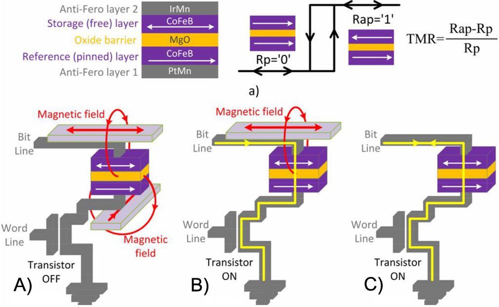
Figure 1.
We observe in the image the three generations of magnetic tunnel junction (MTJs): (A) FIMS; (B) TAS and (C) STT. All cases are denoted as in-plane anisotropy [9].
Figure 1.
We observe in the image the three generations of magnetic tunnel junction (MTJs): (A) FIMS; (B) TAS and (C) STT. All cases are denoted as in-plane anisotropy [9].

The main objective of this publication is to propose an embedded processor evaluation flow based on STT-MRAM for the memory hierarchy. We strongly believe that STT-MRAM could be a valuable memory technology to embed in the next generation of system-on-chip (SoC) . We evaluate STT-MRAM performance, the energy and silicon area and demonstrate that for L1 and L2 , the STT-MRAM brings interesting features for a set of applications. Section 2 describes the methodology flow proposed. Section 3 gives a series of result comparisons between STT-MRAM and SRAM. Section 4 demonstrates that STT-MRAM is a new technology that should be considered for embedded memory hierarchy.
2. Methodology Evaluation Flow
In order to evaluate the impact of STT-MRAM applied in the memory hierarchy, we propose a full methodology flow, as depicted in Figure 2.
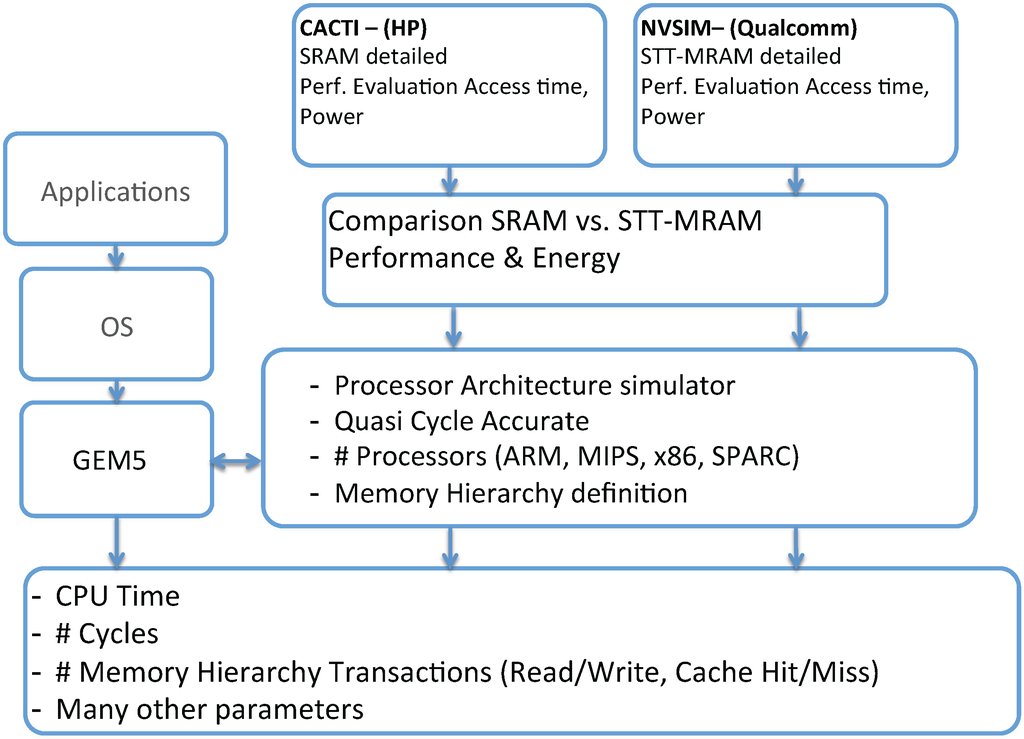
Figure 2.
Evaluation flow.
Figure 2.
Evaluation flow.
For the flow, we defined a processor architectural simulator, in this case, the GEM5 [10]. The GEM5 simulator currently supports a variety of Instruction Set Architecture (ISAs) like Alpha, ARM, MIPS, PowerPC, SPARC and X86. The simulator modularity allows these different ISAs to plug into the generic CPU models and the memory system, without having to specialize one for the other. In our particular case, we adopted the ARM ISA v7 available in GEM5. Specifically, we used the Application Binary Interface (ABI) compatible with the Cortex-A9/A15; our cross-compiler generates binaries specifically for that target.
Our evaluation methodology provides a flow to determine the overall processor system architecture performance, given the memory hierarchy specifications. Tunable parameters include cache size, L1 and L2 latencies and main memory size. Leveraging an architectural simulator, we are able to extract all memory transactions: numbers of read/write accesses into the L1 and L2, cache hits and misses, among other statistical observations. The use of GEM5 (a quasi-cycle accurate simulator) allows us to evaluate different memory sizing strategies, cache policies and the effects of latency at different levels of the memory hierarchy. Combining the memory hierarchy statistics with the intrinsic parameters, we could infer the power consumption, given that one knows the energy cost for the memory bank operation. This way, it is possible to evaluate the overall performance of a built-in SoC using MRAM or SRAM.
Our objective is to compare the use of SRAM against STT-MRAM in the caches of the embedded processor memory hierarchy. For this reason, for SRAM and STT-MRAM, it is necessary to obtain the features of these memories (latency read/write access time, power consumption) to calibrate the GEM5 simulator. For doing this, we pass through our intrinsic analyses flow, which can be performed using NVSim.
For SRAM performances, we can use the memory simulator, CACTI [11,12,13,1415,] or NVSim [16]. CACTI is an integrated simulator, which, based on the technology node, is able to provide accurate information about cache and memory access time, cycle time, area, leakage and the dynamic power model. CACTI was evaluated comparing its results against SPICE simulations.
Concerning STT-MRAM, the memory simulator is based on a modified environment of CACTI: the NVSim simulator [16]. NVSim is a circuit-level model simulator for NVM memory performance, energy and area estimation, which supports various NVM technologies, including STT-RAM, PCRAM, ReRAM and legacy NAND Flash, as well as the SRAM. NVSim was validated comparing its results with industrial NVM prototypes [16], and it is expected to boost architecture-level NVM-related studies.
In the end, we are able to provide for a given application a clear comparison of performance between STT-MRAM and SRAM for an embedded processor architecture. For this article, specifically, we modeled and simulated both SRAM and MRAM using only NVSim. Therefore, all of our physical parameters are generated using NVSim. According to our methodology flow, you can use any one; for us and this publication, we focused on the NVSim only.
3. STT-MRAM vs. SRAM Memory Bank Comparison
In this section, we present our results and analysis comparing the memory intrinsic parameters of STT-MRAM and SRAM. We provide details regarding power, area and an overall performance comparison. A comparison is made between memory banks of equivalent sizes to understand how each technology impacts the performance of the memory hierarchy in a given system. The target technology considered for CMOS and STT-MRAM is a 45 nm node (low-power 45 nm CMOS process (low power performance (LOP))) In Table 2, we provide the technology model features adopted for STT-MRAM and SRAM. Detailed information is available in [17,18].

Table 2.
Memory Cell features models, used to simulate the electrical and physical memory for bank at 45 nm node technology at 300 K of temperature operation.
| STT-MRAM | SRAM | |
|---|---|---|
| Cell Area | 10F2 | 146F2 |
| Aspect Ratio | 1.0 | 1.46 |
| 7100 | ϕ | |
| ϕ | ||
| Read Current | 20μA | ϕ |
| Write Current | 29μA | ϕ |
| Write Pulse | 10ns | ϕ |
| Access CMOS Width | 6F | 1.3F |
| NMOS Width | ϕ | 2.0F |
| PMOS Width | ϕ | 1.2F |
Figure 3, Figure 4, Figure 5, Figure 6, Figure 7 and Figure 8 depict the relations of power, latency, dynamic power, leakage and area for memory banks built using the low power performance (LOP) 45 nm technology process.
In Table 3, depicted in Figure 3, we observe that increases to the memory size correspond to an area increase, as expected. However, the area of SRAM memory banks increases exponentially, while that of STT-MRAM increases linearly. One reason is the memory density: as we double the memory capacity, we indicate that the STT-MRAM density is 10–15 times higher than SRAM density according to [18] (the explanation is in STT-MRAM; the MTJ at 45 nm has an area of 10 F2, while the SRAM cell has 146 F2). Therefore, increases in the amount of memory available for the architecture organization and the impact regarding the density in SRAM are much more critical than with STT-MRAM. They are critical because the slightest increase has an impact on the total die area used, and such an impact using STT-MRAM is not so problematic. To demonstrate this, assume passing cache memory from 2 to 4 MB; in SRAM, we pass from 5.6643 mm2 to 11.2673 mm2, while with STT-MRAM, from 0.6183 mm2 to 0.9958 mm2 assuming only the surface area into account. This same pattern is observed for all of the parameters, with more or less variation according to the parameter.
This comparison is based on the physical parameters of memory banks only, without taking into account bank interconnections at system-level architectures.
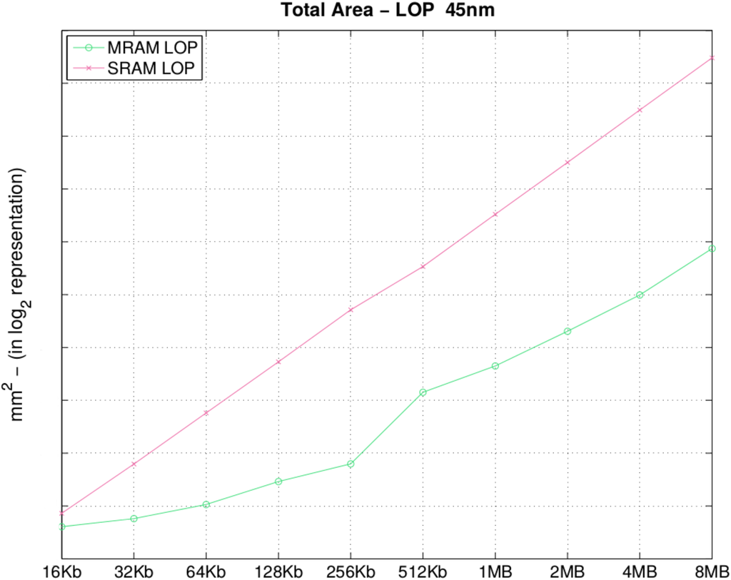
Figure 3.
Total area (mm2).
Figure 3.
Total area (mm2).


Table 3.
Total area (mm2).
| Size | MRAM | SRAM | Size | MRAM | SRAM |
|---|---|---|---|---|---|
| 16 KB | 512 KB | ||||
| 32 KB | 1 MB | ||||
| 64 KB | 2 MB | ||||
| 128 KB | 4 MB | ||||
| 256 KB | 8 MB |
In Figure 4 and Table 4, we observe that the drawback of STT-MRAM memory banks is the write latency, given our model of MTJ. It is a fact that with current STT-MRAM technology, write latency is an issue that jeopardizes the adoption of STT-MRAM into memory hierarchy. In Figure 4, we observe that the write latency gap between STT-MRAM and SRAM is narrowing as we increase the bank size. In Section 4, we evaluate the impact of this latency difference, on an architectural simulator executing an application on top of the memory hierarchy configured according to the presented analysis.
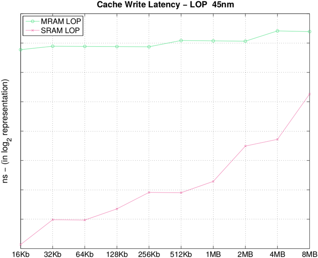
Figure 4.
Cache total write latency (ns).
Figure 4.
Cache total write latency (ns).
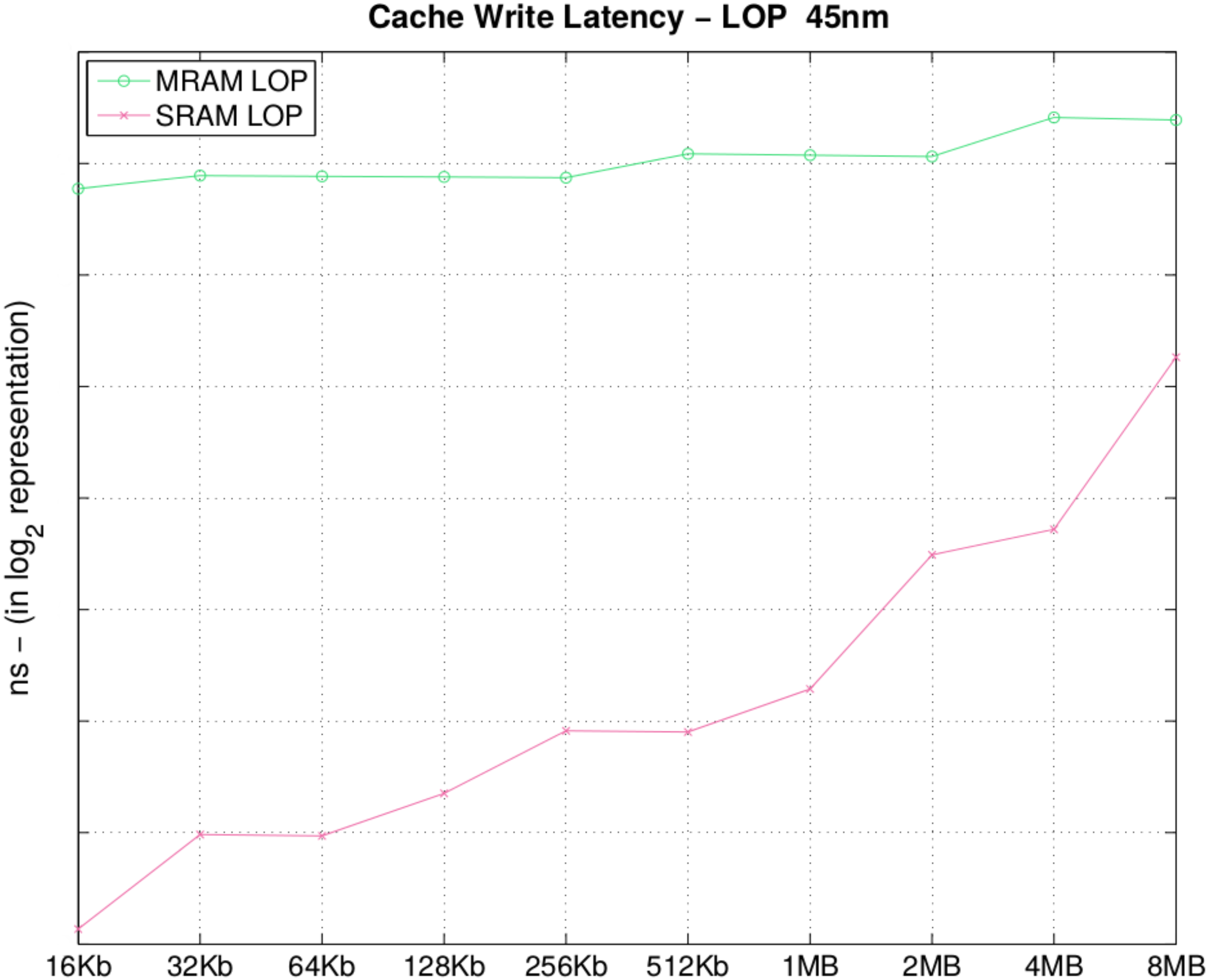

Table 4.
Cache total write latency (ns).
| Size | MRAM | SRAM | Size | MRAM | SRAM |
|---|---|---|---|---|---|
| 16 KB | 109.44 | 1.09 | 512 KB | 135.87 | 3.73 |
| 32 KB | 118.73 | 1.97 | 1 MB | 134.73 | 4.88 |
| 64 KB | 118.20 | 1.95 | 2 MB | 133.60 | 11.24 |
| 128 KB | 117.72 | 2.55 | 4 MB | 170.29 | 13.16 |
| 256 KB | 117.19 | 3.76 | 8 MB | 167.69 | 38.38 |
In Figure 5 and Table 5, we observe one of the major advantages of MRAM, the leakage power, considering both the TAG and DATA arrays of a cachememory set bank. Leakage power is one of the biggest strengths of STT-MRAM technology, which makes it appealing, even with a higher write latency. The main interest in STT-MRAM is that no leakage is induced by the physical device, the MTJ. Given that information is stored only in a magnetic orientation, leakage is created due to the wiring and metal tracks for decoding and sense amplifiers to read the stored information in the STT-MRAM cells. Furthermore, observing Figure 5, one can see that with a 8 MB MRAM, we have almost the same leakage as an SRAM LOP of 128 KB.
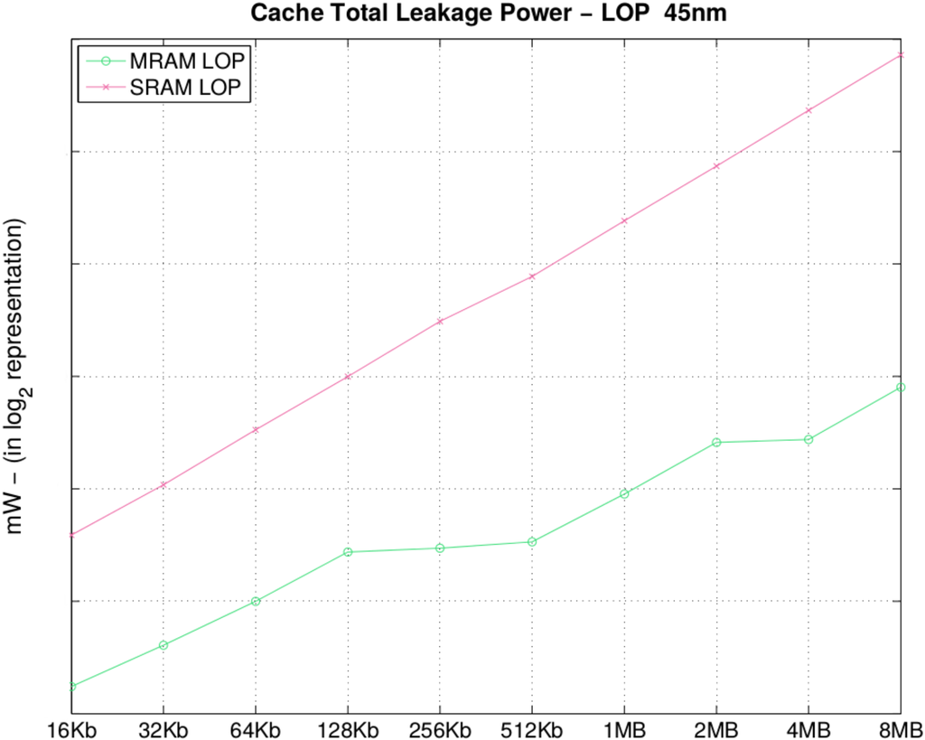
Figure 5.
Cache total leakage power (mW).
Figure 5.
Cache total leakage power (mW).
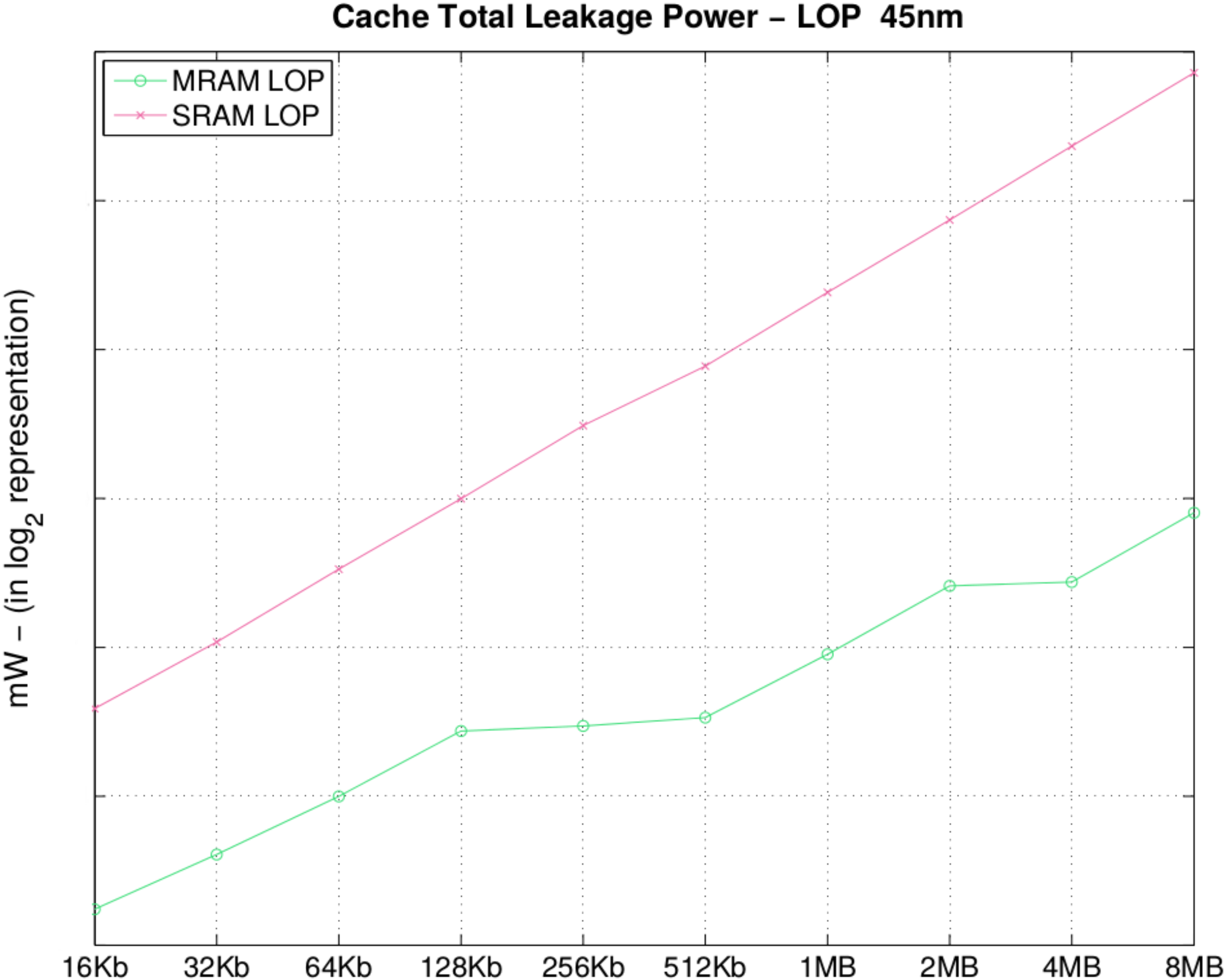

Table 5.
Cache total leakage power (mW).
| Size | MRAM | SRAM | Size | MRAM | SRAM |
|---|---|---|---|---|---|
| 16 KB | 0.02 | 0.14 | 512 KB | 0.13 | 3.42 |
| 32 KB | 0.03 | 0.26 | 1 MB | 0.23 | 6.80 |
| 64 KB | 0.06 | 0.51 | 2 MB | 0.44 | 13.35 |
| 128 KB | 0.11 | 0.99 | 4 MB | 0.45 | 26.57 |
| 256 KB | 0.12 | 1.96 | 8 MB | 0.87 | 52.54 |
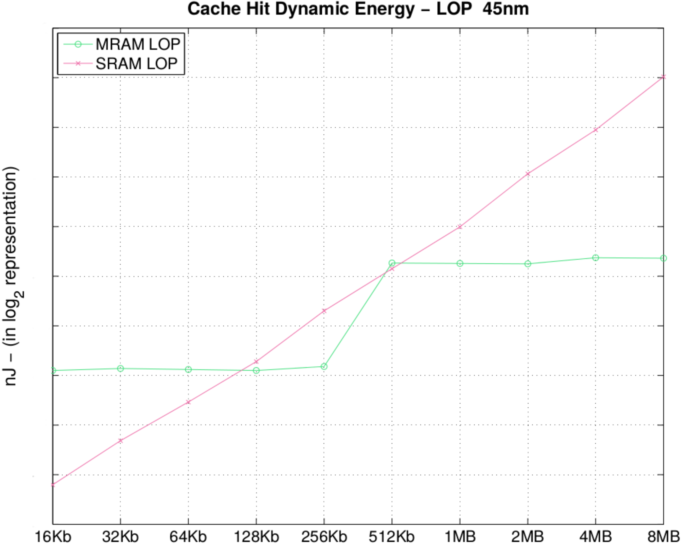
In Table 6 and Figure 6, we present the energy consumption of a hit-access into the cache memory, during the search for the information in the memory bank (disregarding the latency of the Memory Management Unit (MMU) block search). To obtain a hit or even a miss, for an address in the cache, we need to perform a search first in the cache content. Therefore, for the hit, only the read mode is activated, explaining the reason why the cache hit energy is lower for MRAM.

Table 6.
Cache hit dynamic energy (nJ).
| Size | MRAM | SRAM | Size | MRAM | SRAM |
|---|---|---|---|---|---|
| 16 KB | 0.03 | 0.006 | 512 KB | 0.15 | 0.13 |
| 32 KB | 0.03 | 0.01 | 1 MB | 0.14 | 0.24 |
| 64 KB | 0.03 | 0.02 | 2 MB | 0.14 | 0.526 |
| 128 KB | 0.03 | 003 | 4 MB | 0.16 | 0.96 |
| 256 KB | 0.03 | 0.07 | 8 MB | 0.16 | 2.02 |
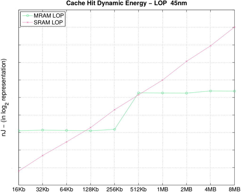
Figure 6.
Cache hit dynamic energy (nJ).
Figure 6.
Cache hit dynamic energy (nJ).
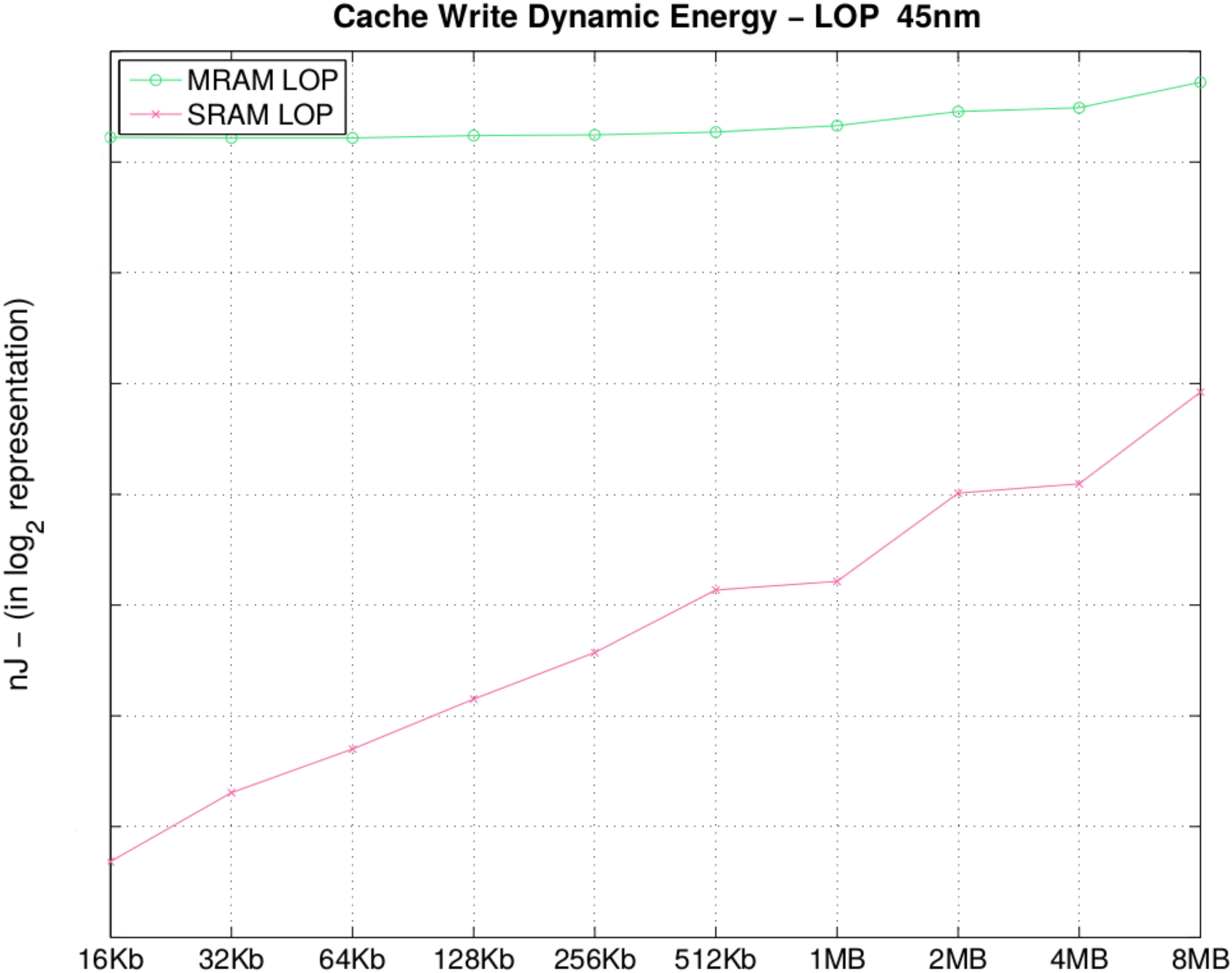
In Table 7 and in Figure 7, we observe that STT-MRAM consumes 91× more dynamic energy for a 16 KB memory bank; when the size of the DATA arrays increases, the difference decreases to 6.9× (in 8 MB) of the write dynamic energy. This is due to the fact that an increase in memory bank size causes a linear increase in dynamic energy for STT-MRAM and an exponential increase when using SRAM. It is important to remark that if we consider the ratio between dynamic energy of 1 MB memory and dynamicenergy of 16 KB memory for STT-MRAM, this ratio is near one. Considering SRAM, this ratio is about six. For the STT-MRAM, the dynamic power consumption is less sensitive to memory size when compared to SRAM. It is easy to identify that the initial energy of STT-MRAM is currently higher than SRAM. However, with the evolution in materials and MTJ manufacturing process, it is expected that the initial dynamic power consumption will decrease to the point where STT-MRAM becomes comparable or even better than SRAM [4,5]. However, for bank sizes larger than 8 MB, the observation is that by increasing the memory bank size, the write dynamic energy of SRAM will become equal to or higher than STT-MRAM at some point. Although the static power consumption is already better than SRAM, the last barriers to STT-MRAM achieving viability of mass employment is the dynamic energy consumption optimization.

Table 7.
Cache write dynamic energy (nJ).
| Size | MRAM | SRAM | Size | MRAM | SRAM |
|---|---|---|---|---|---|
| 16 KB | 0.14 | 0.001 | 512 KB | 0.15 | 0.008 |
| 32 KB | 0.14 | 0.002 | 1 MB | 0.15 | 0.009 |
| 64 KB | 0.14 | 0.003 | 2 MB | 0.17 | 0.01 |
| 128 KB | 0.14 | 0.004 | 4 MB | 0.17 | 0.01 |
| 256 KB | 0.14 | 0.005 | 8 MB | 0.20 | 0.02 |
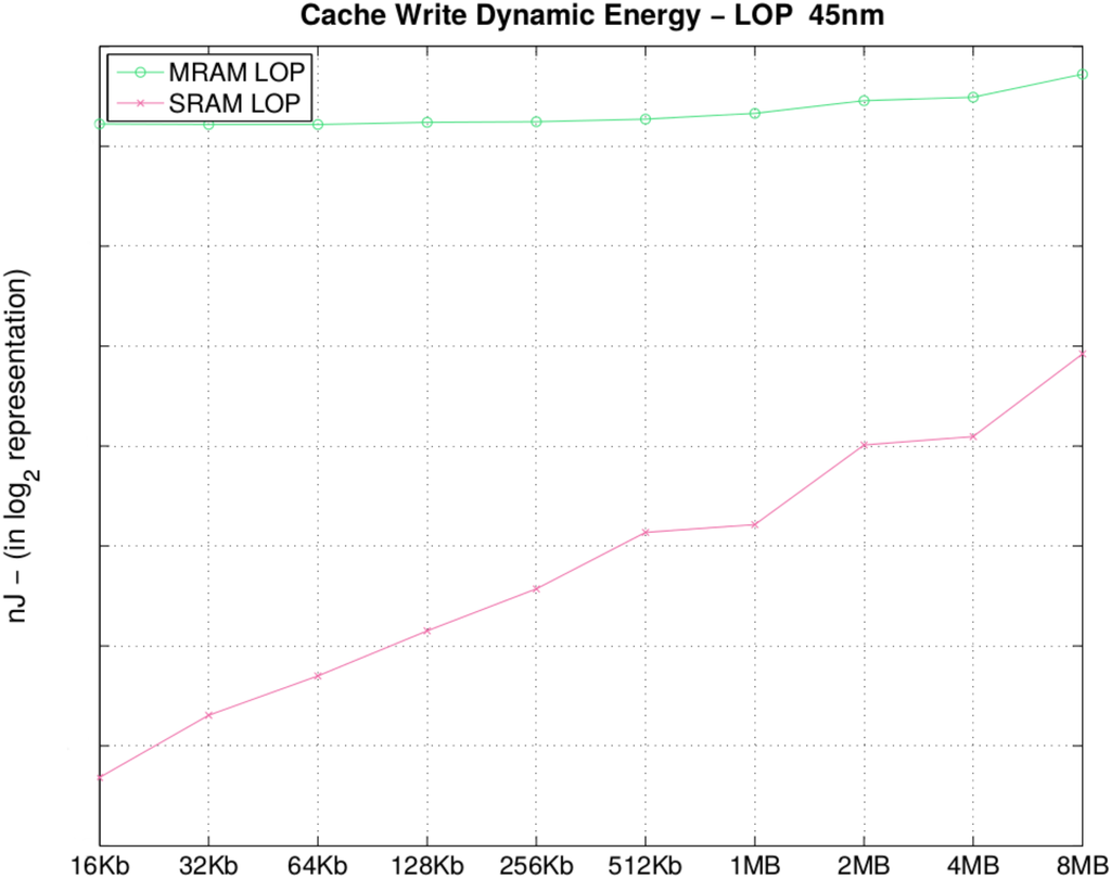
Figure 7.
Cache write dynamic energy (nJ).
Figure 7.
Cache write dynamic energy (nJ).
In this section, we presented the power characteristics of a set of memory banks by comparing STT-MRAM versus SRAM. The obtained results demonstrate that besides the drawbacks regarding latency for writing, STT-MRAM can drastically reduce the power consumption of a cache set memory bank in an embedded system or a high performance system.
Furthermore, the leakage power of an STT-MRAM memory is worth the drawbacks in performance given the gains with power consumption reduction in most of the cases.
In the next section, we are going to apply these results to a real application, demonstrating the performance of STT-MRAM when applied within the memory hierarchy.
4. STT-MRAM Applied in Cache Hierarchy
To evaluate our proposed methodology flow, we present an application case study based on the X.264 video encoder. The processor used for this case study is a 32-bit Reduced Instruction Set Computing (RISC), dual-issue superscalar, out-of-order, speculating dynamic length pipeline (8–11 stages) processor, which is modeled after the ARMv7 architecture. The processor has a clock frequency of 1.5 GHz, and we are running the Linux Operating System on the processor. The video that we wish to encode has a frame rate of 30 FPS and has a resolution of .
We also evaluated the impact of STT-MRAM for L2 cache, and we will compare its characteristics with a similar system employing SRAM. Table 8 summarizes the properties of 45 nm SRAM and STT-MRAM memory banks used as a 2-MB eight-way associative L2 cache. Furthermore, the detailed parameters introduced here were extracted during the intrinsic analysis evaluation discussed in the previous section [17].

Table 8.
Details regarding the architecture and the levels of memory hierarchy.
| Parameter | Features |
|---|---|
| Processor | 32 bits RISC Processor - 8-11 stages pipeline - 2 instructions per cycle |
| L1 Caches | 64 Kbyte SRAM - 4-way set associative, 2 ns access latency - 32 byte per cache line |
| L2 Caches | 2 Mbyte SRAM - 8-way set associative, ∼20 ns access latency - 32 byte per cache line |
The performance comparisons among memory cache banks, eight-way associative, 2-MB SRAM and STT-MRAM in the technology node of 45 nm on L2 cache are described in Table 9.

Table 9.
Memory banks characteristics.
| Field | SRAM | MRAM | |
|---|---|---|---|
| Area | Total area | mm2 | mm2 |
| Data array area | 5 mm2 | mm2 | |
| Tag array area | mm2 | mm2 | |
| Timing | Cache hit latency | 18.8 ns | 70.1 ns |
| Cache miss latency | 2.9 ns | 66.0 ns | |
| Cache write latency | 10.1 ns | 75.1 ns | |
| Power | Hit dynamic energy | 1.07 nJ | 0.213 nJ |
| Miss dynamic energy | 1.07 nJ | 0.213 nJ | |
| Write dynamic energy | 0.03 nJ | 0.22 nJ | |
| Total leakage power | 1326.7 mW | 26.5 mW | |
| Data array leakage Power | 1180.6 mW | 24.3 mW | |
| Tag array leakage Power | 146.1 mW | 2.2 mW | |
| hit(ns) | 18.8 | 70.8 | |
| response (ns) | 10.1 | 75.1 | |
4.1. L2 Cache Exploration for a High Performance System
Considering X.264, the experimental results described in Table 9 are obtained based on the execution of the X.264 benchmark using the Linux OS on top of the Gem5 calibrated with the memory bank latency for each technology.
Based on Table 10, we observe that the total CPU time increases from s to s, which is tolerable for the X.264 application. Given the fact that the STT-MRAM hit latency is 2.7× higher than SRAM, yet we only see a 5% increase in execution time, we conclude that an increased latency of a hit in the L2 cache has a slight impact on the total CPU time.
A major benefit for using STT-MRAM is the lower energy consumption compared to SRAM. STT-MRAM is roughly 50× more energy efficient compared to SRAM, and this is primarily attributed to the lower leakage current of STT-MRAM as seeing in Table 11.

Table 10.
L2-cache dynamic energy estimation.
| SRAM | STT-MRAM | |
|---|---|---|
| CPU time (s) | 16.2 | 17.11 |
| Write back total (Write) | 5,879,046 | 5,944,740 |
| Overall access (Read) | 21,113,987 | 22,309,621 |
| Write energy per cache line | 22.8 nJ | 170.6 nJ |
| Read energy per cache line | 957.7 pJ | 150.4 pJ |
| Total write energy (J) | 0.13 | 1.01 |
| Total read energy (J) | 0.020 | 0.0033 |

Table 11.
Static power consumption.
| SRAM | MRAM | |
|---|---|---|
| Execution time (s) | 16.2 | 17.1 |
| Static power | 1326.7 mW | 26.5 mW |
| Total energy (J) | 21.49 | 0.45315 |
Current implementations of STT-MRAM consume more dynamic energy than SRAM, noted in Table 10. Although STT-MRAM has this disadvantage, STT-MRAM consumes less energy overall when the dynamic and static energy is calculated for our case study. STT-MRAM write operations consume 7.5× more energy than SRAM and 6× more energy for read operations when compared to SRAM. In the case study that we are presenting, STT-MRAM consumes 1.25× more dynamic energy than SRAM for the given workload.
To put our observation in perspective, we look into similar works that achieved similar results through different techniques, like in [19], for example, a 2-MB L2 SRAM cache could be replaced with an 8-MB L2 STT-MRAM cache, using roughly the same silicon die area. In this particular case, the increase on the cache size was not enough to compensate for the penalty, due to the cache access delay. By employing write buffers and a novel cache access policy, the authors managed to achieve a similar performance while reducing the power consumption on the overall application (comprising all of the memory hierarchy) by almost 74%.
They also presented a hybrid MRAM/SRAM cache organization, having 31 sets implemented in STT-MRAM and one set implemented in SRAM. The write-intensive data is kept in the SRAM part, in order to mitigate the higher write delay. A method for determining which datum is suitable for being placed in the SRAM set is also discussed.
In this section, we have demonstrated the interest in using an L2 STT-MRAM cache for high performance applications. In the next section, we will discuss the usage of L1 STT-MRAM cache.
4.2. L1 Cache Exploration for a Low Performance System
Similar to the evaluation of STT-MRAM in a Level-2 cache, we now present an evaluation of STT-MRAM in a Level-1 cache of a microprocessor targeted for an embedded system. Specifically, the target is low performance, where constraints are different, like size, latency, power consumption, but mostly latencies are a predominant factor given the demand for the performance of a CPU. Our goal is to determine if STT-MRAM is a suitable candidate technology to replace SRAM for an L1 cache given that the two share the same silicon fingerprint.
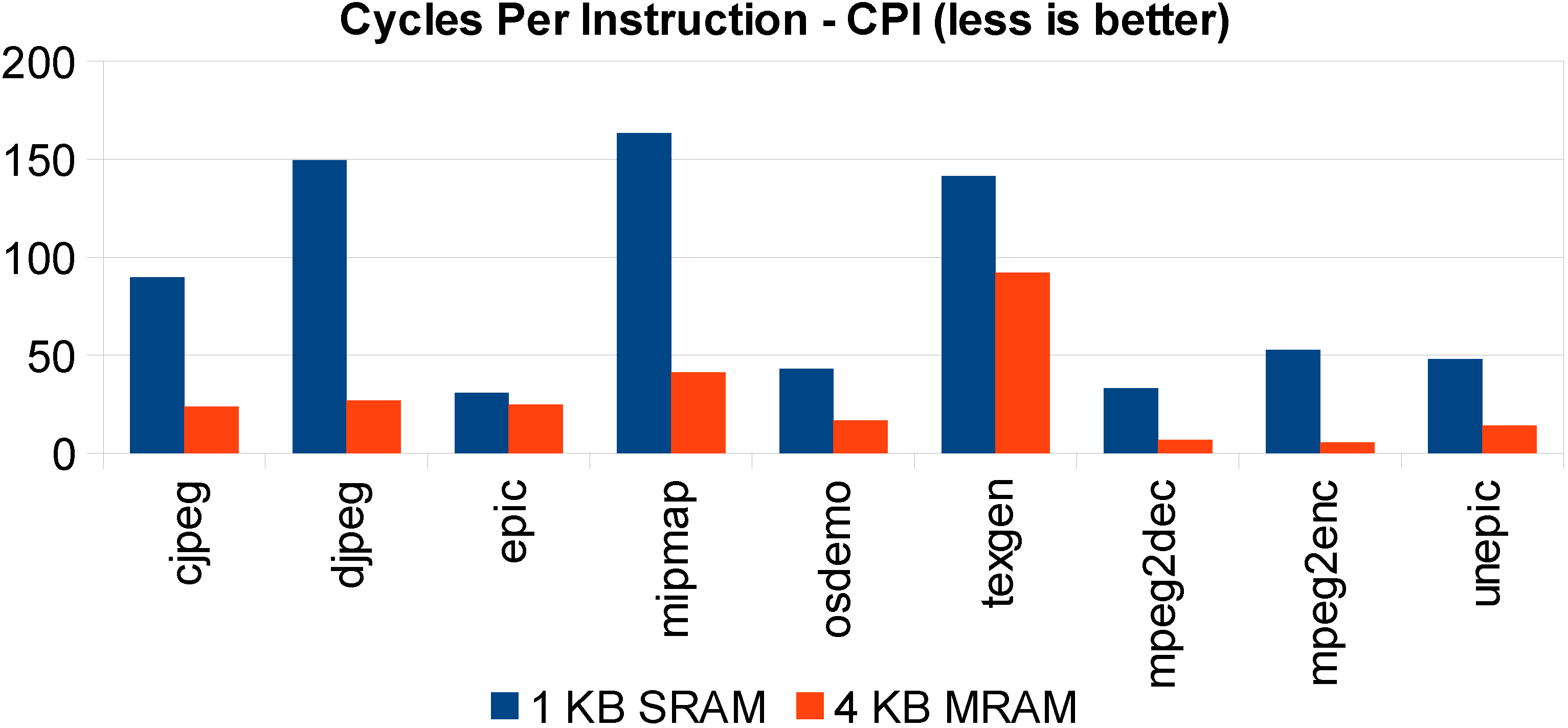
The baseline configuration is quite simple. It consists of a single processor having a single cache level and a large external memory capacity, which is an assumption that can be considered for many systems. In contrast to our previous work in [20], we now assume that the STT-MRAM density is four-times the SRAM [21]. We are then comparing, for instance, a 4-KB SRAM-based cache with a 16-KB MRAM-based cache. For this set of experiments, we assumed a latency of three clock cycles during each cache access. This means that the processor will stall upon each cache request, waiting for the data to become available. We also assumed a latency of 1,000 cycles for the external memory to make the first word available and 10 cycles for each subsequent word, while doing burst reading [22]. In the same manner, as shown in Figure 8, where a 128-KB SRAM cache is compared with its 512-KB STT-MRAM counterpart, the latter shows comparable performance to the smaller, yet faster, SRAM.
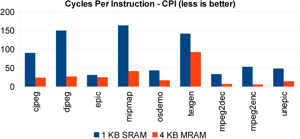
Figure 8.
Same silicon area STT-MRAM versus SRAM L1 cache execution time comparison: 1-KB SRAM versus 4 KB.
Figure 8.
Same silicon area STT-MRAM versus SRAM L1 cache execution time comparison: 1-KB SRAM versus 4 KB.
In Figure 9, we set an STT-MRAM L1 cache of 512 KB, and we compare it with an L1 128-KB SRAM cache size. It is shown that, for most benchmarks, they are comparable in terms of performance.
In order to generalize this conclusion, let us then define the CPI penalty as the increase in the CPI caused by replacing an SRAM cache with an STT-MRAM cache using the same silicon area, as follows:
Based on the Cycles Per Instruction (CPI) penalty (), in Figure 10, the best case, the worst case and the average performance over the benchmark set is shown as a function of the cache capacity. Given that our assumptions are valid, STT-MRAM does present a CPI gain rather than a CPI penalty for most cases. Once the cache capacity is large enough to contain the whole benchmark data, the CPI gain turns into a penalty that can no longer be compensated for if no specific technique is employed.
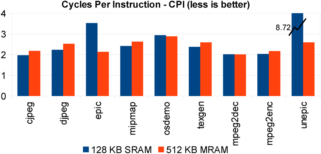
Figure 9.
Same STT-MRAM silicon area versus SRAM L1 cache execution time comparison: 128-KB SRAM versus 512-KB MRAM.
Figure 9.
Same STT-MRAM silicon area versus SRAM L1 cache execution time comparison: 128-KB SRAM versus 512-KB MRAM.

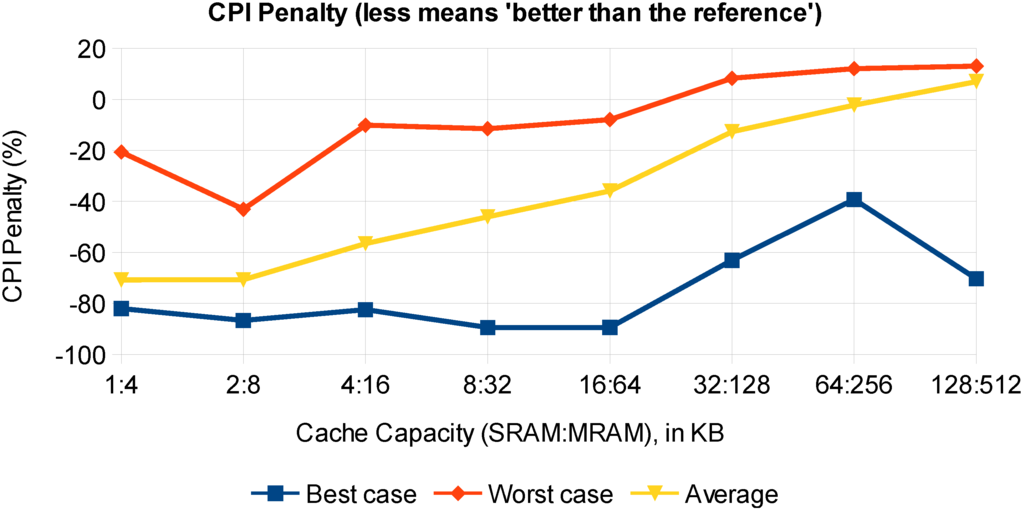
Figure 10.
Overview of the CPI penalty: best case, worst case and average of the Mediabench benchmarks’ performance.
Figure 10.
Overview of the CPI penalty: best case, worst case and average of the Mediabench benchmarks’ performance.

5. Conclusion
In this article, we have demonstrated that STT-MRAM can replace SRAM in the memory hierarchy of a microprocessor. We achieve this conclusion based on our memory hierarchy evaluation methodology flow. Using this flow, we have investigated the performance and power characteristics of STT-MRAM, when used as a replacement for SRAM. Although STT-MRAM has higher latencies, the lower leakage power of STT-MRAM, as compared to SRAM, makes it an attractive candidate replacement technology. Current results indicate that it could be a solution to address the rising power consumption of CMOS circuits. The use of STT-MRAM enables the possibility of new techniques for the implementation of power-saving mechanisms. The non-volatility could be explored to power-off the devices whenever they are idle. Furthermore, non-volatile memory arrays do not need refreshing, reducing the dynamic power and leakage. Independently of our results, the physical properties used in our evaluation of STT-MRAM produce two possible pathways for integrated circuit design. In one, we can conserve the total silicon die area and increase the amount of memory at least four-fold, or we could maintain the same amount of memory, but increase the production yield of the circuit four-fold by switching from SRAM to STT-MRAM. Given our evaluation and the benefits STT-MRAM brings to integrated circuit design, we conclude that STT-MRAM is a strong candidate to replace SRAM in the memory hierarchy of microprocessors.
Acknowledgments
We would like to thank Guillaume Prenat and Gregory Di Pendina, from Spintec at the Commissariat à l’Énergie Atomiquee (CEA) in Grenoble, for their assistance on the physical details regarding the STT-MTJ. ANR, due to the grant of the SPIN and MRAM based Architecture for Reliable and low power Systems (MARS) projects, made this research and all research effort regarding STT-MRAM in France possible. Also, to Adam Manzanares, my colleague for his time reviewing the text, fixing and improving it and suggestions made, that enriched the final text and presentation of this work, Thank you very much Adam.
Author Contributions
Luis Vitorio Cargnini was responsible for the MTJs physics analyses and simulation and STT-MRAM memory banks elaboration. The sections related to architectural evaluation using Gem5, CACTI and NVSim performing the analyses, combining results and compiling the data to put together in this work, also the main text of this publication.
Lionel Torres also worked reviewing and discussing the data from the MTJs regarding the physical aspects and posterior usage to build memory banks, whose data were used into Gem5 for architectural evaluation. He also supervised the work previously done using SuperScalar for the “L1 Cache Exploration for a Low Performance System” section, reviewing this entire work. He is the Spintronics MRAM head researcher at LIRMM.
Raphael Brum was responsible for the section entitled “L1 Cache Exploration for a Low Performance System”, this work began originally with his evaluation using SuperSCalar that later was migrated to Gem5.
Sophiane Senni reviewed the text and the Gem5 analyses, he is currently pursuing the same approach applied to TAS-MRAM.
Gilles Sassatelli has a major involvement in the works using Gem5, regarding the aspects of how to use and add the STT-MRAM banks models in the Gem5 to perform the architectural analyses.
Conflict of Interest
The authors declare no conflict of interest.
References
- Rabaey, J. Low Power Design Essentials; Series on integrated circuits and systems; Springer: Berkeley, California, USA, 2009. [Google Scholar]
- ITRS. Emerging Research Devices; Publisher: New York, USA, 2012; pp. 1–83. [Google Scholar]
- Kim, W.; Park, S.I.; Zhang, Z.; Yang-Liauw, Y. Forming-Free Nitrogen-Doped AlO X RRAM with Sub-μA Programming Current. In Proceedings of the 2011 Symposium on VLSI Technology (VLSIT), Honolulu, HI, USA, 14–16 June 2011.
- Yoda, H.; Fujita, S.; Shimomura, N.; Kitagawa, E.; Abe, K.; Nomura, K.; Noguchi, H.; Ito, J. Progress of STT-MRAM Technology and the Effect on Normally-off Computing Systems. In Proceedings of the 2012 IEEE International Electron Devices Meeting (IEDM), San Francisco, CA, USA, 10–13 December 2012; p. 11.
- Kitagawa, E.; Fujita, S. STT-MRAM cuts power use by 80%. Available online: http://www.eetimes.com/document.asp?doc_id=1280753 (accessed on 13 October 2013).
- Kawahara, T.; Ito, K.; Takemura, R.; Ohno, H. Spin-transfer torque RAM technology: Review and prospect. Microelectron. Reliab. 2012, 52, 613–627. [Google Scholar] [CrossRef]
- Chen, P.; Feng, G.; Shull, R. Use of half metallic Heusler alloys in CoFeB/MgO/Heusler alloy tunnel junctions. IEEE Trans. Magn. 2013, 49, 4379–4382. [Google Scholar] [CrossRef]
- Sterwerf, C.; Meinert, M.; Schmalhorst, J.M.; Reiss, G. High TMR ratio in Co2FeSi and Fe2CoSi based magnetic tunnel junctions. IEEE Trans. Magn. 2013, 49, 4386–4389. [Google Scholar] [CrossRef]
- Singer, P. IEDM: Nanoelectronics provide a path beyond CMOS—ElectroIQ; Extension Media, Solid State Technology: San Francisco, CA, USA, 2012. [Google Scholar]
- Binkert, N.; Sardashti, S.; Sen, R.; Sewell, K.; Shoaib, M.; Vaish, N.; Hill, M.D.; Wood, D.A.; Beckmann, B.; Black, G.; et al. The Gem5 simulator. ACM SIGARCH Comput. Archit. News 2011, 39, 1–7. [Google Scholar] [CrossRef]
- Wilton, S.J.; Jouppi, N.P. An Enhanced Access and Cycle Time Model for on-Chip Caches; Digital Western Research Laboratory (HP): Palo Alto, California, USA, 1993. [Google Scholar]
- Muralimanohar, N.; Ahn, J.H.; Jouppi, N.P. Memory Modeling with CACTI. In Processor and System-on-Chip Simulation; Leupers, R., Temam, O., Eds.; Springer Science + Business Media LLC: Cambridge, Massachusetts, USA, 2010; Vol. III, pp. 229–242. [Google Scholar]
- Muralimanohar, N.; Balasubramonian, R.; Jouppi, N.P. CACTI 6.0: A Tool to Model Large Caches. In Proceedings of the International Symposium on Microarchitecture, Chicago, IL, USA, April 21 2009.
- Reinman, G.; Jouppi, N.P. CACTI 2.0: An Integrated Cache Timing, Power, and Area Model; Technical report; Compaq Computer Corporation Western Research Laboratory: Palo Alto, CA, USA, February 2000. [Google Scholar]
- Shivakumar, P.; Jouppi, N.P. CACTI 3.0: An Integrated Cache Timing, Power, and Area Model; Technical report; Compaq Computer Corporation Western Research Laboratory: Palo Alto, CA, USA, 2001. [Google Scholar]
- Dong, X.; Xu, C.; Xie, Y.; Jouppi, N.P. NVSim: A circuit-level performance, energy, and area model for emerging nonvolatile memory. IEEE Trans. Comput.-Aided Des. Integr. Circuits Syst. 2012, 31, 994–1007. [Google Scholar] [CrossRef]
- Cargnini, L.V. MRAM Applied to Embedded Processors Architecture and Memory Hierarchy. Ph.D. Thesis, Laboratoire de Informatique, Robotique et Microelectronique de Montpellier (LIRMM) Université de Montpellier (UM2), Montpellier, France, 2013. [Google Scholar]
- Kang, S.H. Embedded STT–MRAM for Mobile Applications: Enabling Advanced Chip Architectures; Qualcomm Inc., University of California: San Diego, CA, USA, 11–13 April 2010; pp. 1–23. [Google Scholar]
- Sun, G.; Dong, X.; Xie, Y.; Li, J.; Chen, Y. A Novel Architecture of the 3D Stacked MRAM L2 Cache for CMPs. In High Performance Computer Architecture; HPCA: Raleigh, NC, USA, 14–18 February 2009; pp. 239–249. [Google Scholar]
- Zhao, W.; Zhang, Y.; Lakys, Y.; Klein, J.O.; Etiemble, D.; Revelosona, D.; Chappert, C.; Torres, L.; Cargnini, L.; Brum, R.; et al. Embedded MRAM for High-Speed Computing. In Proceedings of the IEEE/IFIP 19th International Conference on VLSI and System-on-Chip (VLSI-SoC), Hong Kong, China, 3–5 October 2011; pp. 37–42.
- Mackay, K. TAS, TAS+STT-MRAM and Magnetic Logic Unit; Technical report; Crocus Technology, e-NVM conference: Gardanne, Provence-Alpes-Côte d’Azur, France, 2011. [Google Scholar]
- JEDEC Solid State Technology Association. Double Data Rate (DDR) SDRAM Standard; JESD79F; JEDEC Committee JC-42.3; JEDEC: Arlington, VA, USA, February 2008. [Google Scholar]
© 2014 by the authors; licensee MDPI, Basel, Switzerland. This article is an open access article distributed under the terms and conditions of the Creative Commons Attribution license (http://creativecommons.org/licenses/by/4.0/).
