Abstract
The global variability of ultra-thin body and buried oxide (UTBB) MOSFETs in subthreshold and off regimes of operation is analyzed. The variability of the off-state drain current, subthreshold slope, drain-induced barrier lowering (DIBL), gate leakage current, threshold voltage and their correlations are considered. Two threshold voltage extraction techniques were used. It is shown that the transconductance over drain current (gm/Id) method is preferable for variability studies. It is demonstrated that the subthreshold drain current variability in short channel devices cannot be described by threshold voltage variability. It is suggested to include the effective body factor incorporating short channel effects in order to properly model the subthreshold drain current variability.
1. Introduction
Ultra-thin body and buried oxide (UTBB) technology is promising for future MOSFET nodes due to its short channel effects immunity [1] and low variability [2]. The quantification of global variability improves fabrication process optimization and MOSFET model extraction. Whereas threshold voltage variability has been widely studied [3,4,5], subthreshold variability has received little attention. Characterization of subthreshold variability has become essential nowadays. Design is shifting towards the subthreshold regime for low power applications. Furthermore, the off-state drain current variability is important for stand-by power considerations.
The variability of MOSFET parameters is due to geometry fluctuations, the granularity of materials and doping randomness [6]. Doping randomness affects MOSFET variability through random dopant fluctuations (RDF) in the channel, the source and drain extensions and in the ground plane. Fabrication imperfections cause the variability of device dimensions, such as line edge roughness (LER), as well as Si channel and buried oxide (BOX) thicknesses. The granularity of gate material also contributes to the parameter variability of a device. Typically, the channel of an FD SOI device (including UTBB) is left undoped, thus eradicating RDF in the channel. In general, well-controlled process, small, short channel effects [3] and low series resistance [7] contribute to the low variability of FD SOI [1,2,5,7].
The aim of the study is to perform a qualitative analysis of global subthreshold parameter variability. Such an analysis can be carried out even on devices that are not yet fully optimized from the short channel effects perspective. The parameters of interest for the subthreshold regime are the off-state drain current (Id-off) and gate current (Ig-off), threshold voltage (Vth), subthreshold slope (S) and drain-induced barrier lowering (DIBL). The off-state currents were extracted at gate voltage Vg = 0 V. Absolute values of the correlation coefficients are presented in this work. This paper is an extended version of our previous work [8]. It also incorporates some results from [9]. The data from [9] were improved by doubling the number of characterized devices, thus enhancing statistics.
2. Experimental Details
The devices studied in this work are fully-depleted (FD) silicon-on-insulator (SOI) n-channel MOSFETs fabricated on 25 nm-thick BOX. The top Si layer is 7.5 nm-thick. The channel is left undoped allowing the avoidance of RDF. The n-type ground plane was incorporated below BOX. The equivalent oxide thickness of the gate dielectric is 1.2 nm. Devices with gate lengths Lg from 28 to 88 nm and a gate width Wg of 10 µm are characterized. 106 transistors of each gate length are measured across the wafer. A 3-sigma normality test was carried out to exclude outliers.
Two threshold voltage extraction techniques are used in this work: using the constant current method, Vth is obtained as Vg, where Id/(Wg/Lg)) = 10−7 A; the transconductance over drain current (gm/Id) method is described in [10,11,12]. Both extraction methods are widely used in the linear and saturation regimes of operation.
3. Results and Discussion
Figure 1 shows the ratios of standard deviations (σ) to mean values (μ) of Id-off, S, DIBL and Vth extracted using the gm/Id technique at drain voltages Vd of 1 V and 20 mV. As expected, shorter devices exhibit stronger variation in both regimes of operation. It can be seen that Id-off variability is rather strong and presumably impacted by the variability of other parameters (e.g., Vth, S and DIBL).
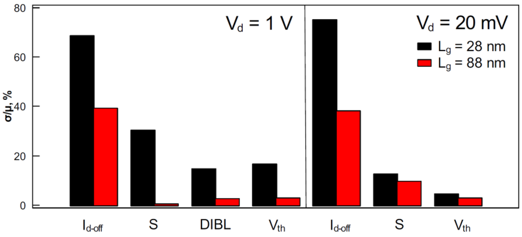
Figure 1.
The ratio of standard deviation over the mean value of the off-state drain current (Id-off), subthreshold slope (S), drain-induced barrier lowering (DIBL) and threshold voltage (Vth) extracted using the gm/Id method in devices with gate lengths of 28 and 88 nm.
Figure 1.
The ratio of standard deviation over the mean value of the off-state drain current (Id-off), subthreshold slope (S), drain-induced barrier lowering (DIBL) and threshold voltage (Vth) extracted using the gm/Id method in devices with gate lengths of 28 and 88 nm.

3.1. Off-State Gate Current
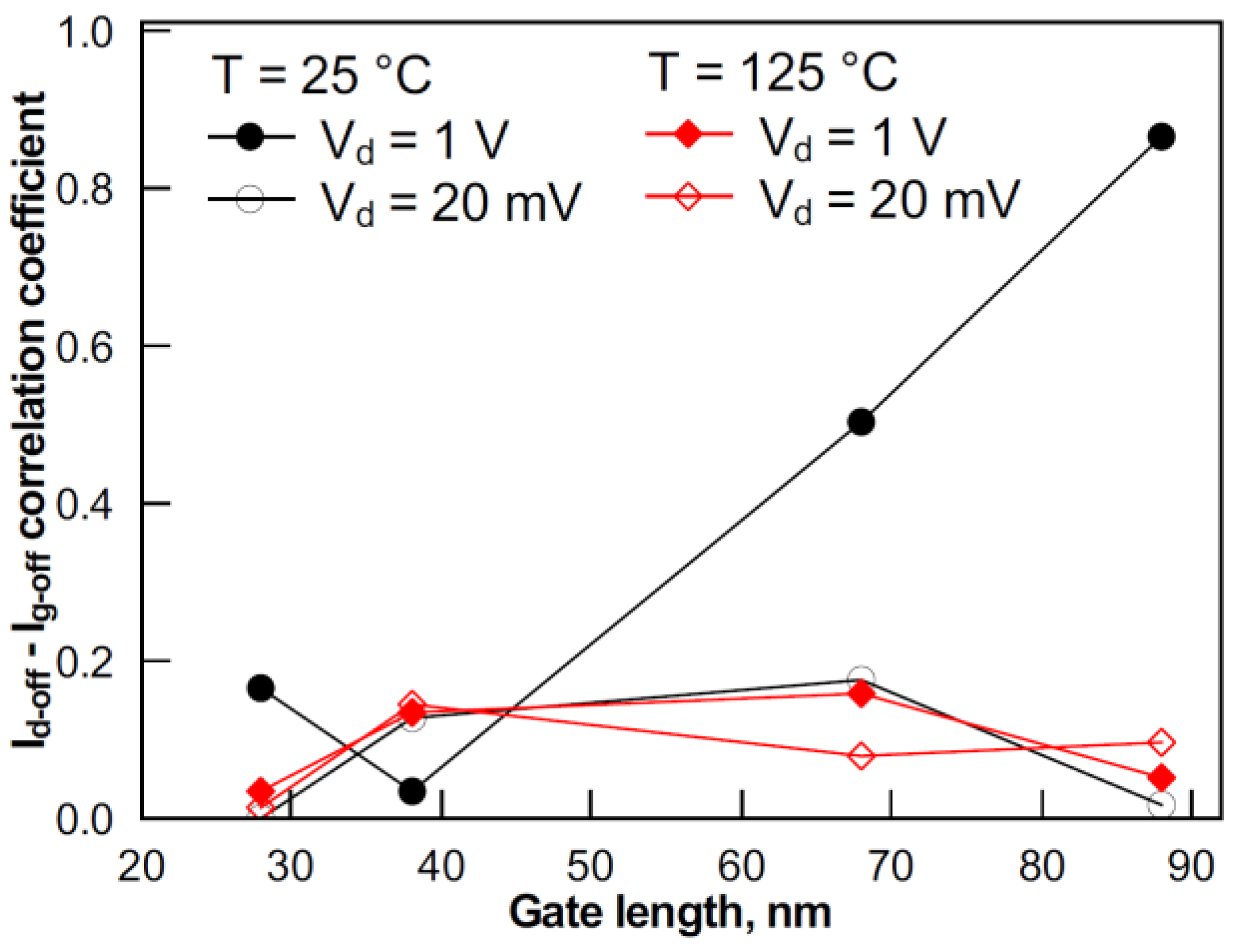
Figure 2 shows σId-off in devices with gate lengths from 28 nm to 88 nm in linear and saturation regimes. The higher variability of Id-off is observed in shorter devices. Different parameters, such as short channel effects, Ig and Vth, have an impact on Id in the off-state.
First, Ig-off is considered. The standard deviation of Ig-off is shown in Figure 2. An increase of σIg-off with Vd can be related to the amplified generation current, which is a function of Vd [13]. There is no pronounced dependence of Ig-off variability on the gate length. Furthermore, σIg-off remains small compared with σId-off, except for the longest devices at Vd of 1 V. Absolute values of Ig-off are also negligibly small compared with Id-off (except for devices with a gate length of 88 nm at Vd of 1 V). Therefore, the effect of Ig-off variability on Id-off is expected to be negligible. In order to confirm this, Figure 3 plots coefficients of correlation between Ig-off and Id-off for devices with various gate lengths at Vd of 1 V and 20 mV and at temperatures of 25 and 125 °C. Only in the case of Vd of 1 V and a temperature of 25 °C does the correlation become stronger with a gate length increase as the Ig-off component of Id-off increases. Ig-off is small at low Vd, as the gate-induced drain leakage (GIDL) is alleviated. This is confirmed by weak Ig-off and Id-off correlation at Vd of 20 mV for all gate lengths. With a temperature rise, due to Vth shift and S degradation, Id increases stronger than Ig. Thus, the effect of Ig on Id decreases, and the correlation between Id-off and Ig-off reduces (Figure 3). The above discussion suggests that the effect of Ig-off variability on Id-off variability should be accounted for only in relatively long devices at high Vd and room temperature, whereas in other cases, it can be neglected.
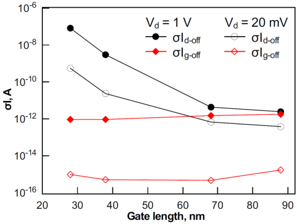
Figure 2.
σId-off and σIg-off variations with gate length at drain voltages (Vd) of 20 mV and 1 V.
Figure 2.
σId-off and σIg-off variations with gate length at drain voltages (Vd) of 20 mV and 1 V.
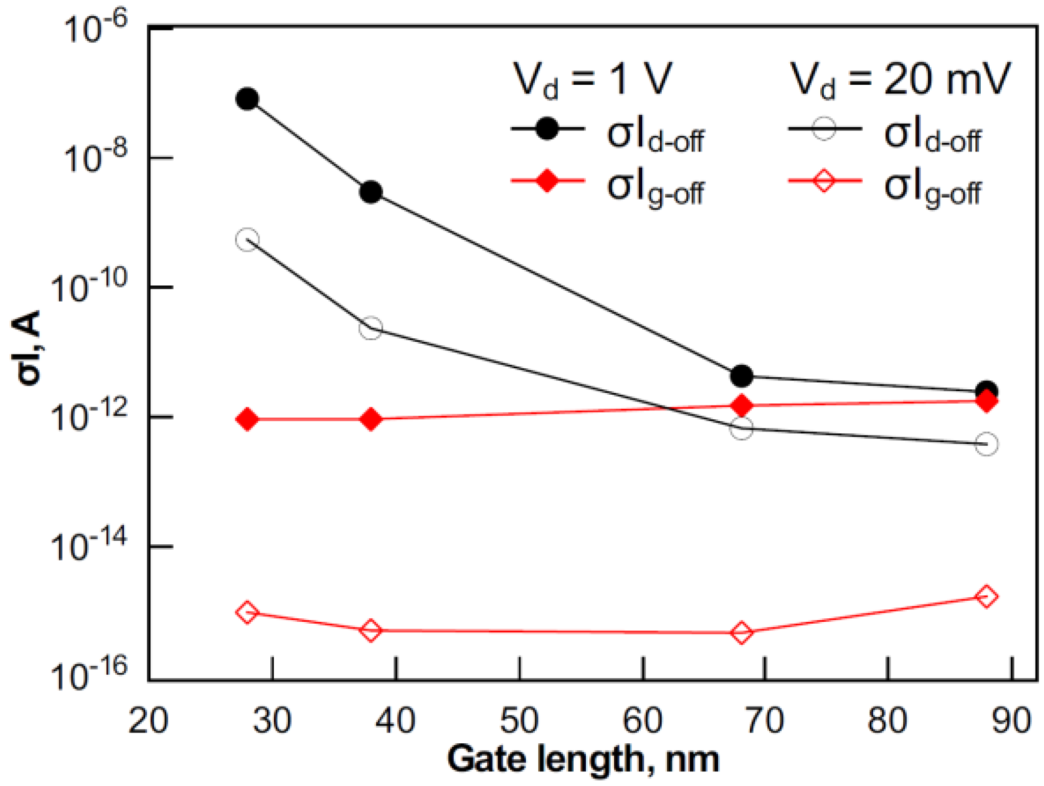

Figure 3.
The Id-off-Ig-off correlation in devices with various gate lengths at Vd of 20 mV and 1 V and temperatures of 25 °C and 125 °C.
Figure 3.
The Id-off-Ig-off correlation in devices with various gate lengths at Vd of 20 mV and 1 V and temperatures of 25 °C and 125 °C.
3.2. Threshold Voltage
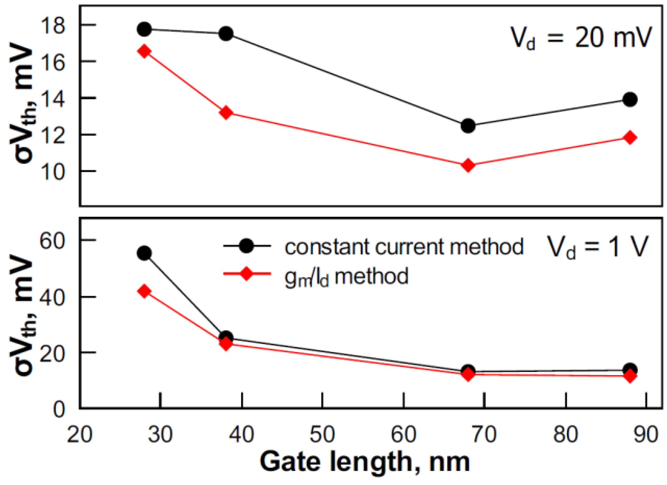
Secondly, the effect of Vth variability on σId-off is considered. Figure 4 shows σVth for devices with gate lengths from 28 to 88 nm at Vd of 20 mV and 1 V. The variability in shorter devices is obviously stronger than in long devices. At Vd of 1 V, σVth is larger than at Vd of 20 mV in short devices. However, in long devices, values of σVth are similar in both regimes of operation. At Vd of 1 V in the shortest devices, σVth is considerably different for two Vth extraction methods. The gm/Id method results in a lower Vth variability than the constant current method. This is due to Vth extraction from different parts of current-voltage characteristics and the smaller sensitivity of the gm/Id method to short channel effects (S, DIBL), as discussed in [9]. This difference vanishes in long devices.

Figure 4.
σVth obtained using the constant current and gm/Id methods at Vd of 20 mV (top); and Vd of 1 V (bottom).
Figure 4.
σVth obtained using the constant current and gm/Id methods at Vd of 20 mV (top); and Vd of 1 V (bottom).
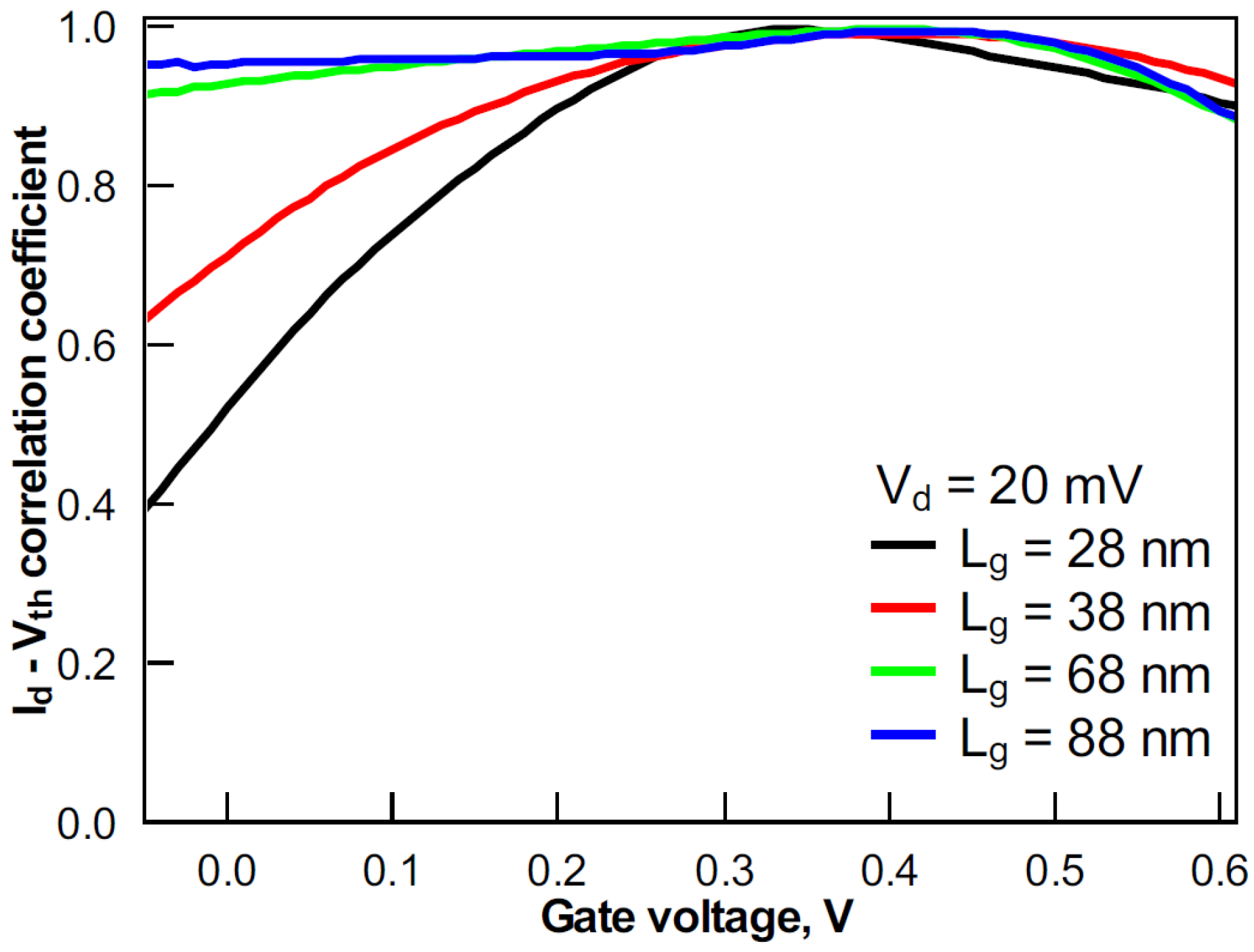
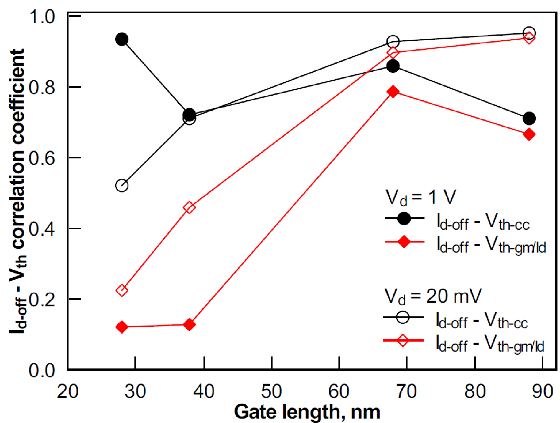
Since in the subthreshold regime, Id exponentially depends on Vth, it is generally assumed that σId in this region is dominated by σVth. This holds true for the relatively long devices studied in this work. Correlation between Id-off and Vth at Vd of 1 V is plotted in Figure 5 for 28 nm- and 100 nm-long devices. Vth was extracted using the constant current and gm/Id methods. To quantify the correlation, Figure 6 plots the coefficients of correlation between Id and Vth (extracted using the constant current method) as a function of Vg in devices with various gate lengths. In the subthreshold region, correlation is strong for 68 and 88 nm-long devices. In strong inversion, the correlation reduces due to the dominance of mobility and series resistance variability [13]. However, in shorter devices, the Id and Vth correlation significantly decreases, not only in strong inversion, but also in the subthreshold regime. This effect is also seen in Figure 7, where variation of the Id-off and Vth correlation coefficients with the gate length is plotted. Therefore, the variability of other parameters apart from Ig-off and Vth has to be taken into account.

Figure 5.
The variation of Id-off at Vd = 1.0 V with Vth extracted using the constant current and gm/Id methods at Vd = 1 V in devices with gate lengths of 28 nm and 88 nm.
Figure 5.
The variation of Id-off at Vd = 1.0 V with Vth extracted using the constant current and gm/Id methods at Vd = 1 V in devices with gate lengths of 28 nm and 88 nm.
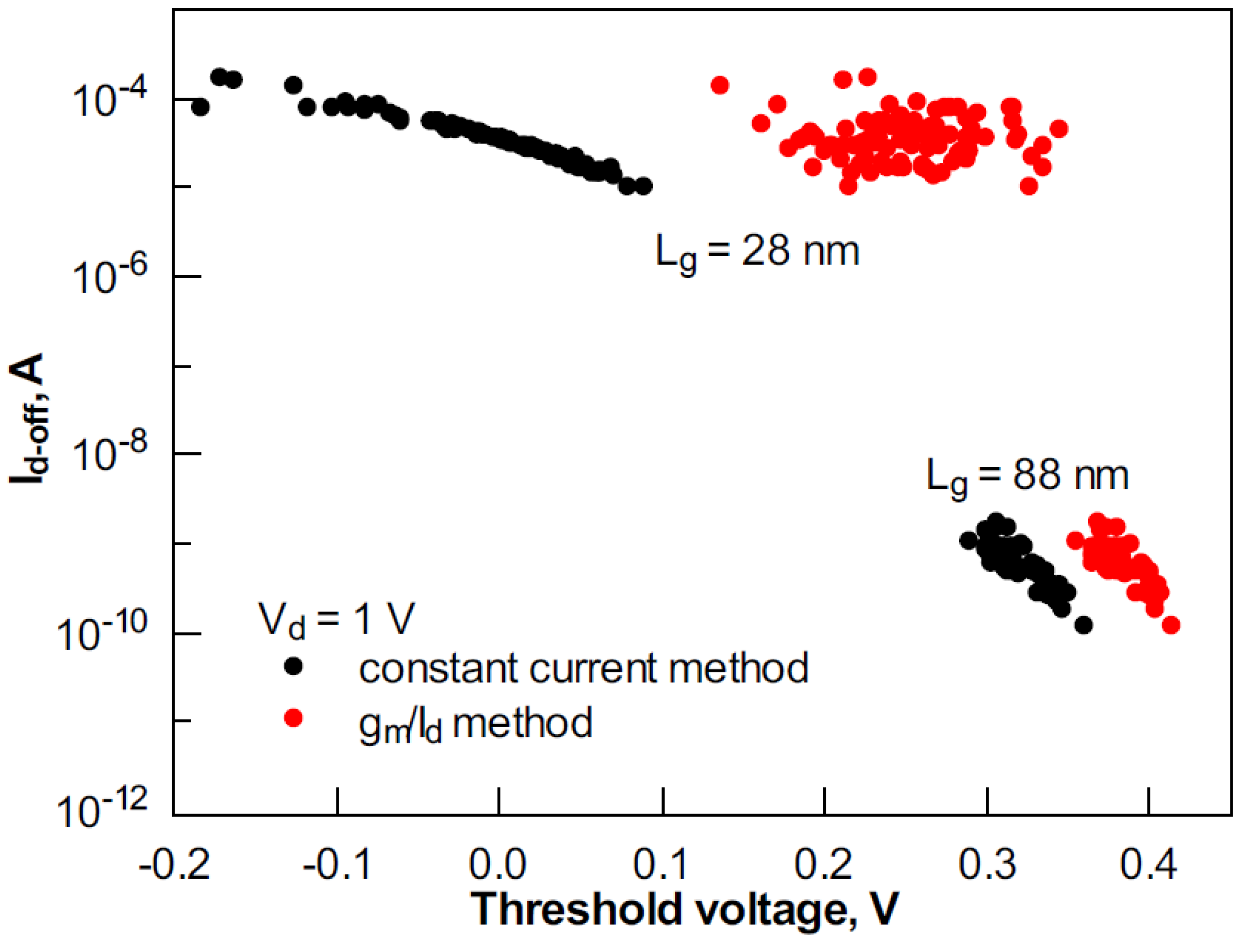

Figure 6.
The variation of the Id-Vth correlation coefficient with Vg in devices with various gate lengths. Vth was obtained using the constant current method.
Figure 6.
The variation of the Id-Vth correlation coefficient with Vg in devices with various gate lengths. Vth was obtained using the constant current method.
It is important to note the importance of the Vth extraction method in variability studies. In [9], it was shown that the gm/Id Vth extraction method is beneficial over other techniques from the short channel effects perspective. A similar property can be observed in Figure 7. The low correlation of Vth‑gm/Id and Id-off in short devices suggests the parasitic effect immunity of Vth extraction using the gm/Id technique [11,12] compared with the constant current method, as the latter is obviously sensitive to DIBL [9].

Figure 7.
The Vth-Id-off correlation coefficients in devices with various gate lengths. Vth was obtained using the constant current (cc) and gm/Id methods.
Figure 7.
The Vth-Id-off correlation coefficients in devices with various gate lengths. Vth was obtained using the constant current (cc) and gm/Id methods.
3.3. Short Channel Effects
Thirdly, an impact of short channel effect variability on subthreshold Id is considered. The data in Figure 8 show strong correlation between Id-off and DIBL in shorter devices. The correlation coefficient decreases to ~0.2 and even more for devices with gate lengths of 68 nm and 88 nm, where the average DIBL is below 60 mV/V. Correlation between Id-off and Vth (extracted at Vd of 20 mV) featured an opposite trend increasing with the gate length, as seen from Figure 7. Therefore, in devices with gate lengths of 68 and 88 nm, Id-off and Vth variability is caused by the same mechanisms, while the variability of DIBL and subthreshold slope dominates in short devices.

Figure 8.
The DIBL-Id-off correlation coefficients in devices with various gate lengths.
Figure 8.
The DIBL-Id-off correlation coefficients in devices with various gate lengths.
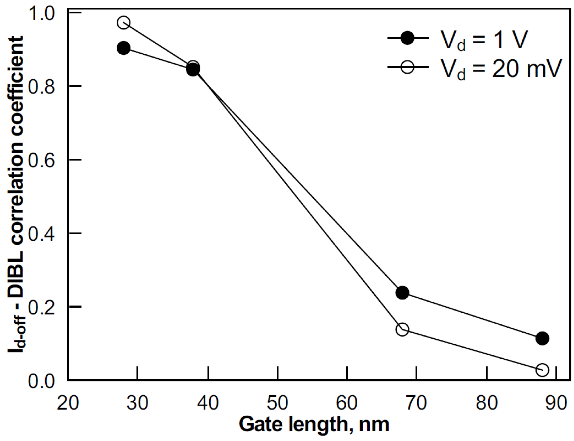
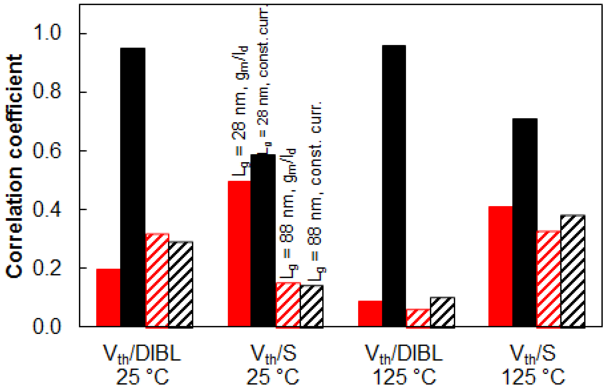
Figure 9 presents the variation of the subthreshold slope and Vth extracted using the constant current and the gm/Id methods, at high Vd in saturation. Scatter is much stronger in short devices than in longer ones, as expected. Furthermore, in short devices, the correlation of the subthreshold slope with Vth-cc is stronger than the correlation with Vth-gm/Id. This correlation is quantified in Figure 10. Figure 10 shows DIBL and Vth, as well as the S and Vth correlation in 28 nm- and 88 nm-long devices at 25 °C and 125 °C. Vth was extracted with the gm/Id and constant current methods. Vth extracted using the gm/Id technique shows little dependence on short channel effects, even at high temperatures. Vth obtained with the constant current method shows very strong correlation with DIBL at room and elevated temperatures. This comparison confirms that the gm/Id technique enables an evaluation of intrinsic Vth, only slightly affected by short channel effects. Evaluation of Vth free of short channel effects is of interest for device models that incorporate variability. If variability is imposed on each of the correlating parameters in a model, the total performance variability might be overestimated [9]. This can be avoided either by including correlation factors in the models or using independent (zero correlation) parameters.

Figure 9.
Variations of Vth obtained using the gm/Id and constant current methods as a function of the subthreshold slope.
Figure 9.
Variations of Vth obtained using the gm/Id and constant current methods as a function of the subthreshold slope.
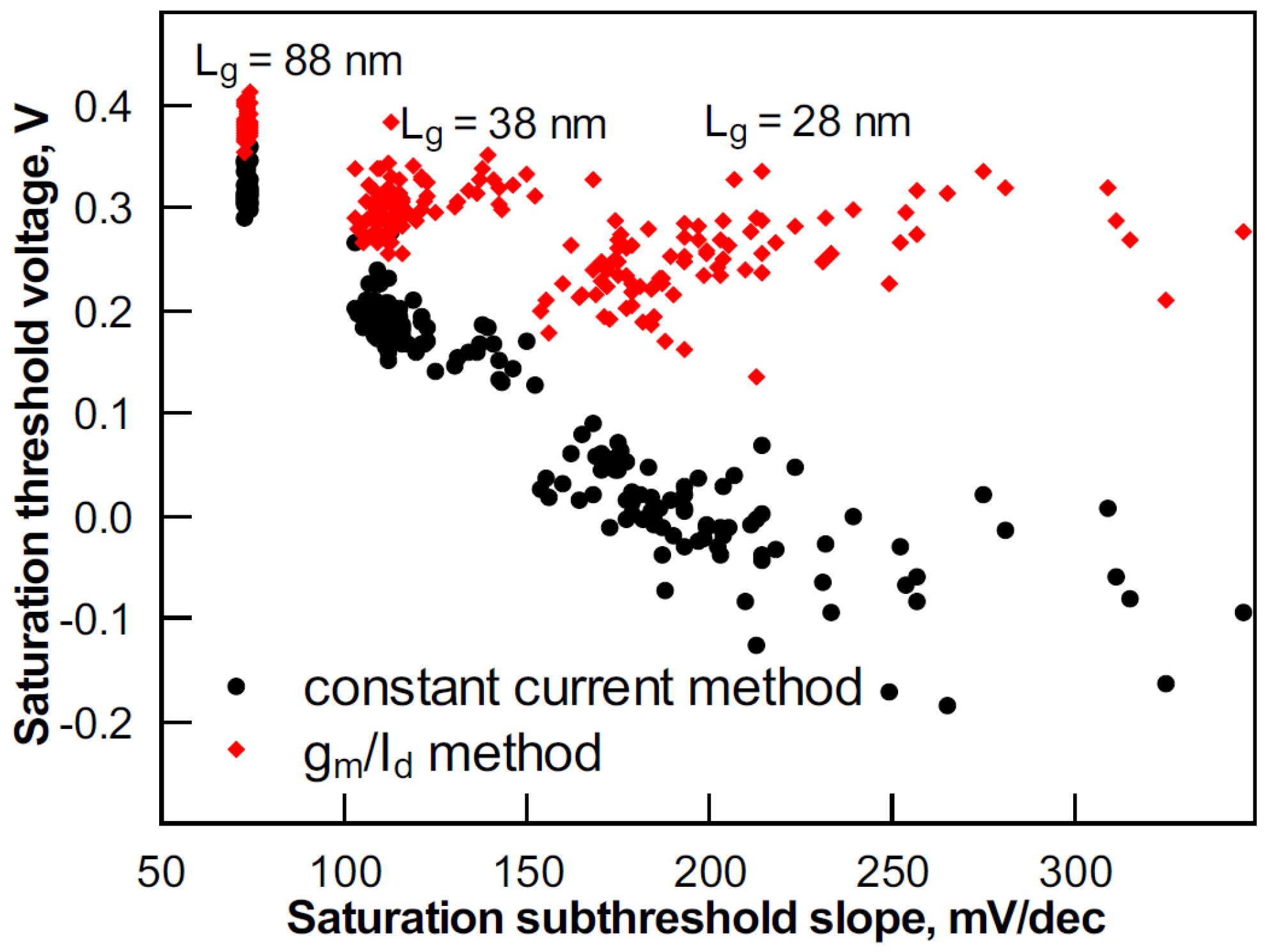

Figure 10.
The Vth-DIBL and Vth-S correlation coefficients in devices with gate lengths of 28 nm and 88 nm at 25 °C and 125 °C temperatures. Vth was obtained using the constant current and gm/Id methods.
Figure 10.
The Vth-DIBL and Vth-S correlation coefficients in devices with gate lengths of 28 nm and 88 nm at 25 °C and 125 °C temperatures. Vth was obtained using the constant current and gm/Id methods.
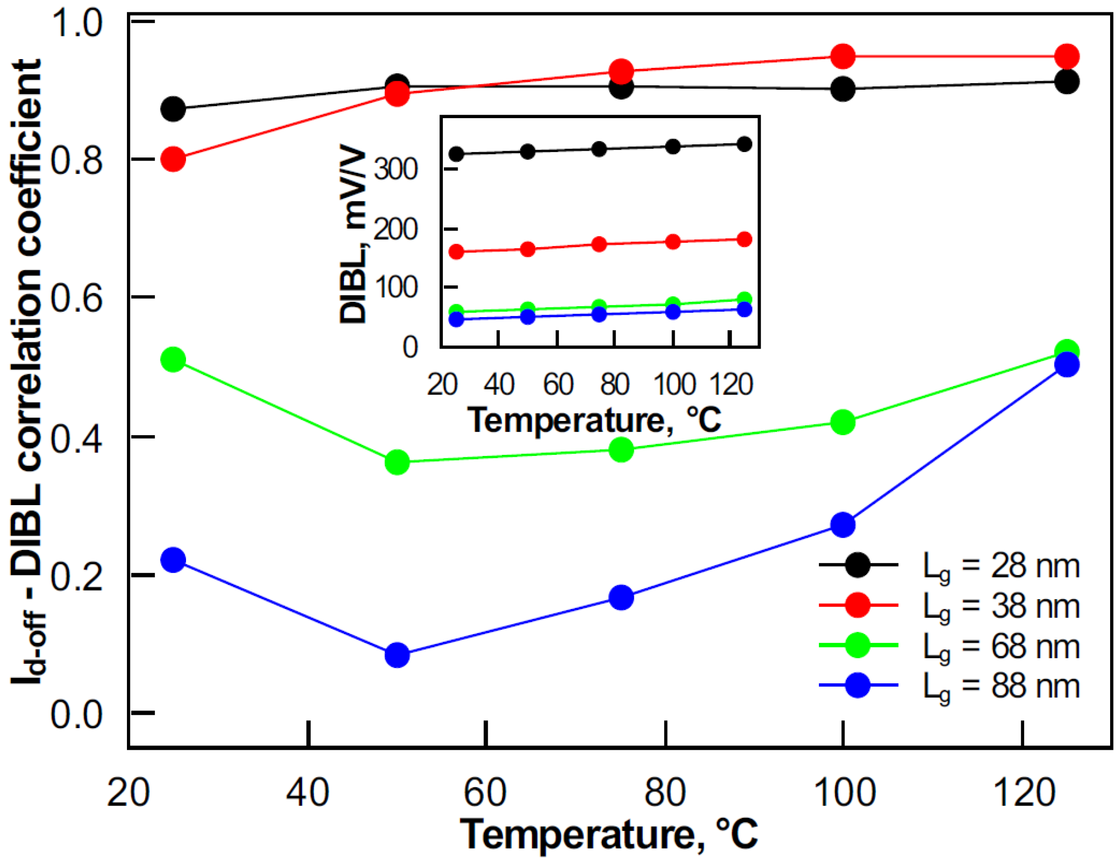
The temperature dependence of the Id-off and DIBL correlation is shown in Figure 11. In the case of short devices (gate lengths of 28 nm and 38 nm), the correlation factor being very strong shows nearly no dependence on temperature. However, in long devices (gate lengths of 68 nm and 88 nm), the correlation between Id-off and DIBL rises with temperature. This can be explained by the DIBL increase with temperature, as the inset in Figure 11 shows.
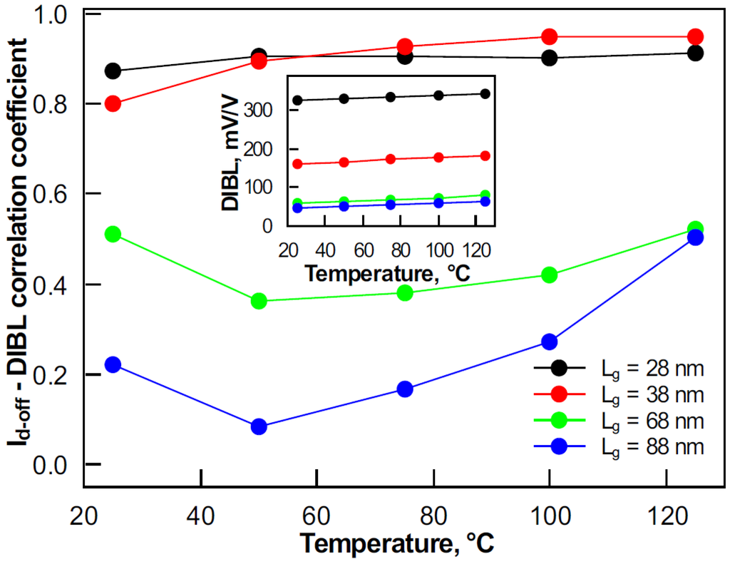
Figure 11.
The Id-off–DIBL correlation in devices with various gate lengths in the 25–125 °C temperature range at Vd of 1 V. The inset shows the DIBL temperature dependence.
Figure 11.
The Id-off–DIBL correlation in devices with various gate lengths in the 25–125 °C temperature range at Vd of 1 V. The inset shows the DIBL temperature dependence.
3.4. Drain Current Variability Modelling
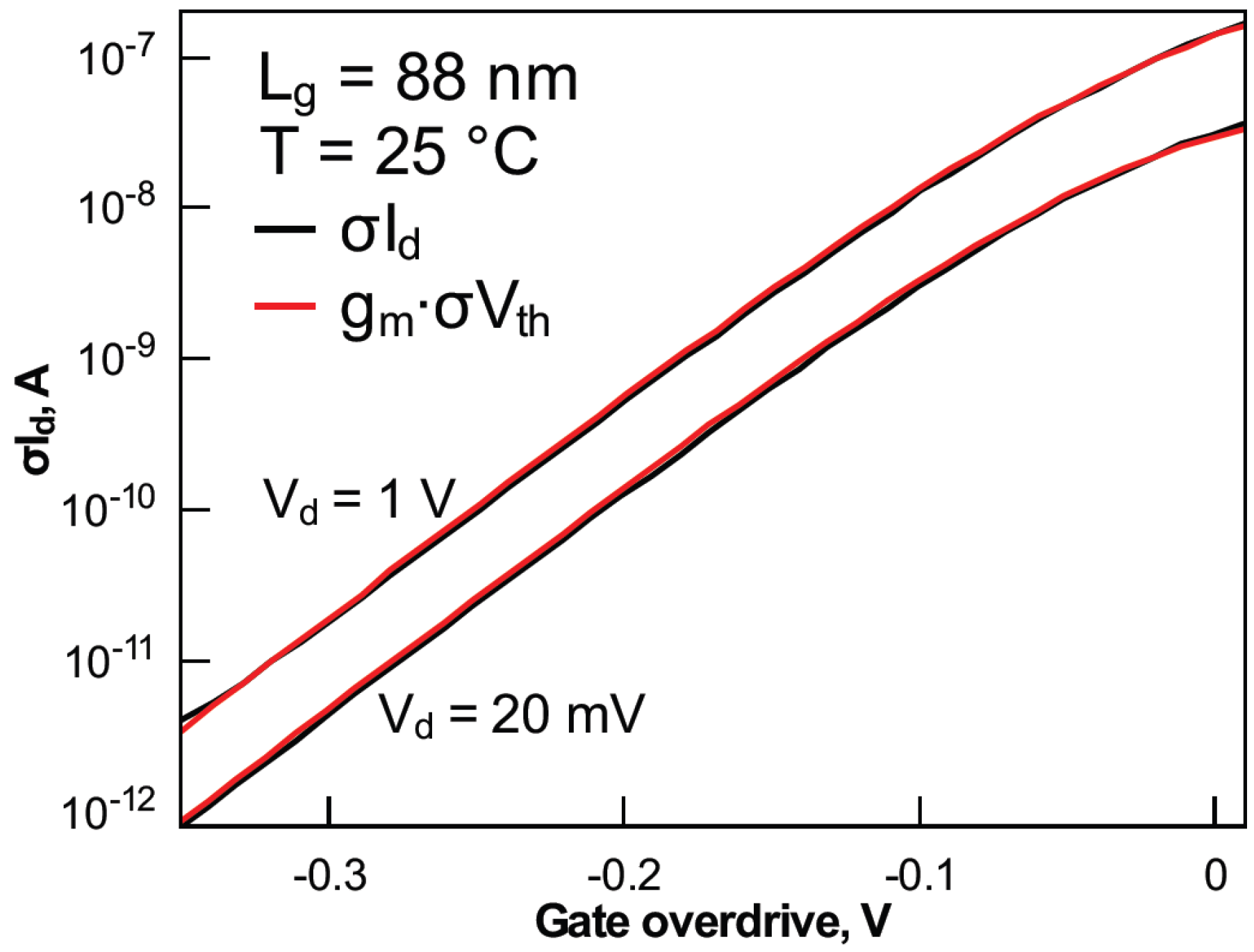
Following the above discussion, Figure 12 compares σId and gm·σVth dependences on Vg in devices with a gate length of 88 nm at Vd of 1 V and 20 mV. σId agrees well with gm·σVth in around-threshold and subthreshold regions, i.e., moderate and weak inversion. In order to ease the comparison of devices with different gate lengths and at various temperatures, the results are plotted as a function of the gate overdrive Vg–Vth.

Figure 12.
Variation of σId and its components with gate overdrive at Vd of 20 mV and 1 V at 25 °C in devices with a gate length of 88 nm. Vth was extracted using the gm/Id method.
Figure 12.
Variation of σId and its components with gate overdrive at Vd of 20 mV and 1 V at 25 °C in devices with a gate length of 88 nm. Vth was extracted using the gm/Id method.
The situation is different in short channel devices. As seen from Figure 13, σId can be described by gm·σVth only in a very narrow Vg range around Vth. In the subthreshold, the curves strongly deviate. In [14], it was suggested to consider the variability of the body factor in weak inversion in addition to Vth. The impact of the body factor dependences on Vg and temperature was emphasized and related to depletion width variation [14]. The UTBB devices studied here remain fully-depleted in the whole weak-to-moderate inversion range at any temperature. Furthermore, Si and oxide thickness fluctuations are not significant, due to the well-controlled fabrication process [2,9]. In [2], reflectometry was used to evaluate top silicon layer thickness variability and correlate it with electrically obtained data. Furthermore, in [9], it was found that global variability does not degrade with temperature through Si layer thickness variation, confirming that the process matches σId sufficiently well (Figure 12). As this is not the case in the shortest device (Figure 13), we consider the effective body factor n, which includes short channel effects. Thus, in our case, n dependence on Vg originates from the gate and the drain counteraction on electrostatics. In this work, n (Vg) is derived in the first approximation from S(Vg) according to
, where q is the elementary charge, k is the Boltzmann constant and T is the temperature. At Vd of 20 mV, the combined effect of σVth and σn can fit σId sufficiently well:
However at Vd of 1 V, Equation (1) does not allow one to fit σId. This is due to amplification of short channel effects at Vd of 1 V and, thus, their stronger impact on Vth. In order to fit σId, Vth and n, correlation coefficient ρ has to be accounted for:
This approach is shown to work sufficiently well at elevated temperature. In Figure 14, it is shown that σId at 125 °C is fitted well when the Vg-dependent effective body factor and its correlation with the Vth are considered (Equation (2)).
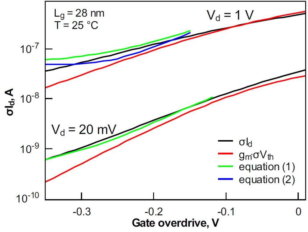
Figure 13.
Variation of σId and its components with gate overdrive at Vd of 20 mV and 1 V at 25 °C in devices with a gate length of 28 nm. Vth was extracted using the gm/Id method.
Figure 13.
Variation of σId and its components with gate overdrive at Vd of 20 mV and 1 V at 25 °C in devices with a gate length of 28 nm. Vth was extracted using the gm/Id method.

The results presented in Figure 12, Figure 13 and Figure 14 were obtained using the gm/Id Vth extraction technique. Figure 15 shows σId fitting in 28 nm-long devices at 25 °C with Vth obtained using the constant current method. The fitting is acceptable at Vd of 20 mV, as short channel effects are not strongly pronounced. However, at Vd of 1 V, the fitting works only in a very narrow Vg region close to Vth. This can be explained by the strong impact of short channel effects on the constant current extraction of Vth. This again confirms the advantages of the gm/Id Vth extraction method for variability assessment.
Further σId modelling improvement can be done by accounting for GIDL in the very low Vg region. In strong inversion, mobility and series resistance should be considered [13].

Figure 14.
Variation of σId and its components with gate overdrive at Vd of 20 mV and 1 V at 125 °C in devices with a gate length of 28 nm. Vth was extracted using the gm/Id method.
Figure 14.
Variation of σId and its components with gate overdrive at Vd of 20 mV and 1 V at 125 °C in devices with a gate length of 28 nm. Vth was extracted using the gm/Id method.
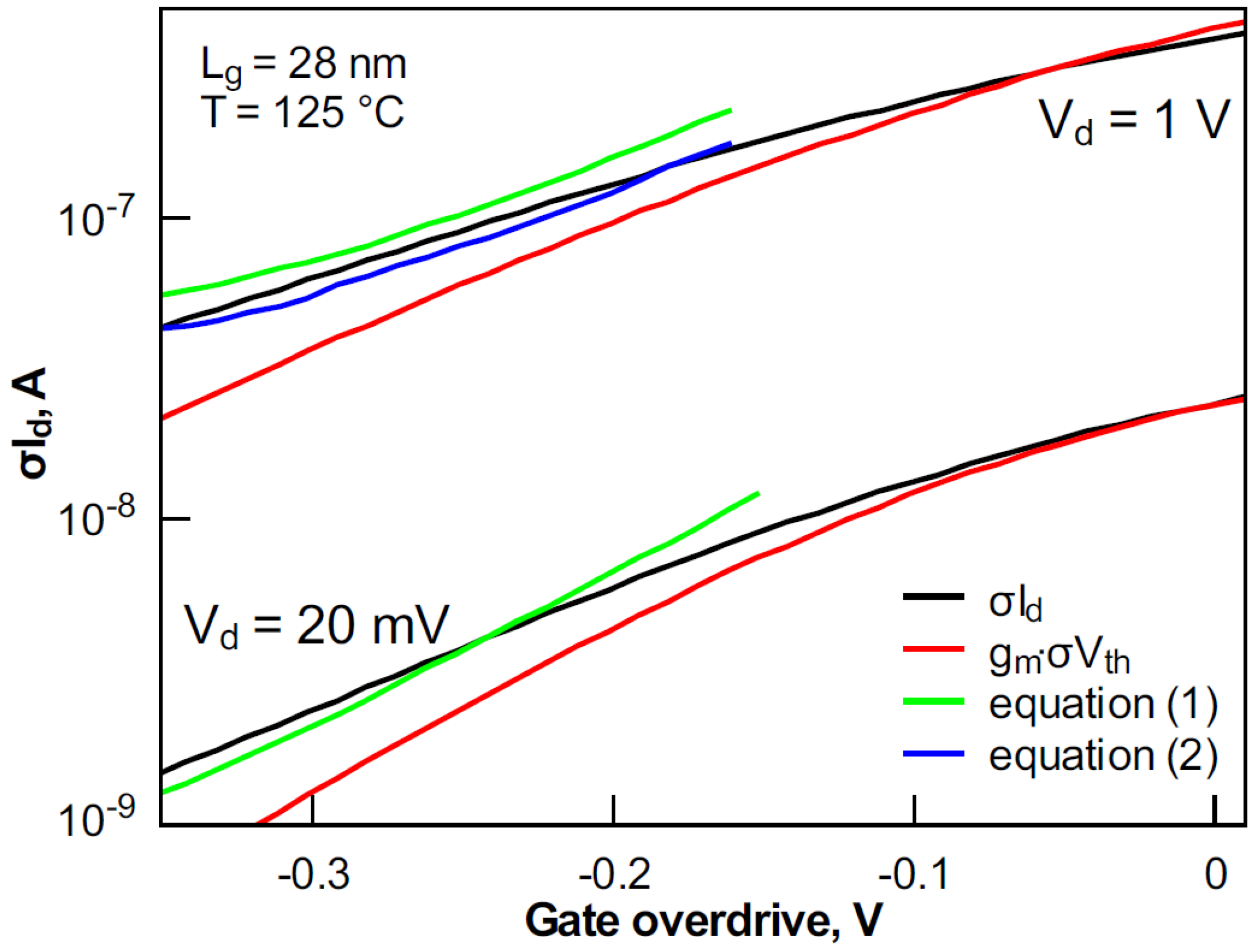
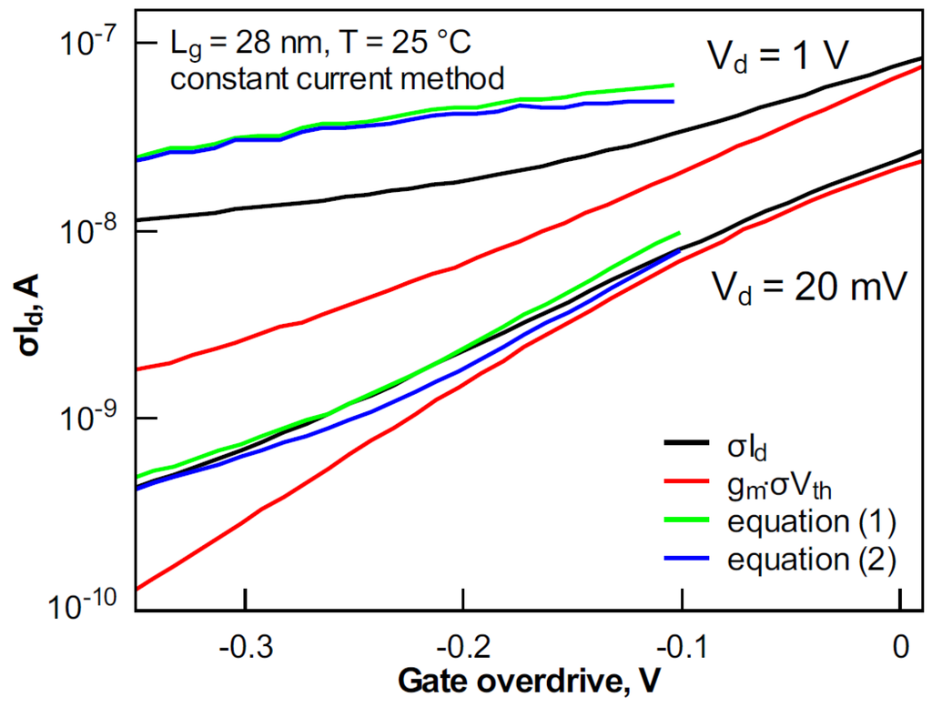
Figure 15.
Variation of σId and its components with gate overdrive at Vd of 20 mV and 1 V at 25 °C in devices with a gate length of 28 nm. Vth was extracted using the constant current method.
Figure 15.
Variation of σId and its components with gate overdrive at Vd of 20 mV and 1 V at 25 °C in devices with a gate length of 28 nm. Vth was extracted using the constant current method.

4. Conclusions
The global variability of UTBB devices in the subthreshold has been analyzed through Id-off, Ig-off, S, Vth, DIBL and their correlations. A generally used approach to model σId using σVth is shown to work well for long devices. For short channel devices, an improved procedure that accounts for the Vg-dependent effective body factor (incorporating short channel effects) was proposed and validated in the temperature range from 25 °C to 125 °C. This is important for power consumption considerations and compact model parameter extraction in the off-regime. It was shown that the gm/Id Vth extraction technique is beneficial for accurate variability assessment and modeling.
Acknowledgments
The research was partially funded by FNRS (Fonds National de la Recherche Scientifique), Belgium, Catrene “Reaching 22” and FP7 NoE “Nanofunction”.
Author Contributions
Sergej Makovejev, Jean-Pierre Raskin, Denis Flandre and Valeriya Kilchytska performed in-depth analysis and contributed to paper writing. Babak Kazemi Esfeh performed measurements and the initial results analysis. François Andrieu provided devices for this work.
Conflicts of Interest
The authors declare no conflict of interest.
References
- Liu, Q.; Yagishita, A.; Loubet, N.; Khakifirooz, A.; Kulkarni, P.; Yamamoto, T.; Cheng, K.; Fujiwara, M.; Cai, J.; Dorman, D. Ultra-Thin-Body and BOX (UTBB) Fully Depleted (FD) device integration for 22 nm node and beyond. Symp. VLSI Technol. 2010, 61–62. [Google Scholar] [CrossRef]
- Weber, O.; Faynot, O.; Andrieu, F.; Buj-Dufournet, C.; Allain, F.; Scheiblin, P.; Foucher, J.; Daval, N.; Lafond, D.; Tosti, L.; et al. High Immunity to Threshold Voltage Variability in Undoped Ultra-Thin FDSOI MOSFETS and Its Physical Understanding. In Proceedings of the International Electron Devices Meeting IEDM, San Francisco, CA, USA, 15–17 December 2008.
- Sugii, N.; Tsuchiya, R.; Ishigaki, T.; Morita, Y. Local Vth variability and scalability in silicon-on-thin-box (SOTB) CMOS With small random-dopant fluctuation. IEEE Trans. Electron. Devices 2010, 57, 835–845. [Google Scholar] [CrossRef]
- Khakifirooz, A.; Cheng, K.; Kulkarni, P.; Cai, J.; Ponoth, S.; Kuss, J.; Haran, B.S.; Kimball, A.; Edge, L.F.; Reznicek, A.; et al. Challenges and Opportunities of Extremely Thin SOI (ETSOI) CMOS Technology for Future Low Power and General Purpose System-on-Chip Applications. In Proceedings of the International Symposium on VLSI Technology, Systems and Applications, Hsin Chu, Taiwan, 26–28 April 2010; pp. 110–111.
- Mazurier, J.; Weber, O.; Andrieu, F.; Toffoli, A.; Rozeau, O.; Poiroux, T.; Allain, F.; Perreau, P.; Fenouillet-Beranger, C.; Thomas, O.; et al. On the variability in planar FDSOI technology: From MOSFETs to SRAM cells. IEEE Trans. Electron. Devices 2011, 58, 2326–2336. [Google Scholar] [CrossRef]
- Asenov, A.; Cheng, B. Modeling and simulation of statistical variability in nanometer CMOS technologies. In Analog Circuit Design; Casier, H., Steyaert, M., van Roermund, A.H.M., Eds.; Springer: Dordrecht, The Netherlands, 2011. [Google Scholar]
- Mazurier, J.; Weber, O.; Andrieu, F.; Allain, F.; Tosti, L.; Brévard, L.; Rozeau, O.; Jaud, M.-A.; Perreau, P.; Fenouillet-Beranger, C.; et al. Drain Current Variability and MOSFET Parameters Correlations in Planar FDSOI Technology. In Proceedings of the International Electron Devices Meeting IEDM, San Francisco, CA, USA, 15–17 December 2008; pp. 575–578.
- Makovejev, S.; Esfeh, B.K.; Andrieu, F.; Raskin, J.; Flandre, D.; Kilchytska, V. Global Variability of UTBB MOSFET in Subthreshold. In Proceedings of the IEEE SOI-3D-Subthreshold Microelectronics Technology Unified Conference, Monterey, CA, USA, 7 October 2013.
- Makovejev, S.; Kazemi Esfeh, B.; Raskin, J.-P.; Flandre, D.; Kilchytska, V. Threshold Voltage Extraction Techniques and Temperature Effect in Context of Global Variability in UTBB MOSFETs. In Proceedings of the European Solid-State Device Research Conference ESSDERC, Venice, Italy, 16–20 September 2013.
- Flandre, D.; Kilchytska, V.; Rudenko, T. gm/Id Method for threshold voltage extraction applicable in advanced MOSFETs with nonlinear behavior above threshold. IEEE Electron. Device Lett. 2010, 31, 930–932. [Google Scholar] [CrossRef]
- Rudenko, T.; Kilchytska, V.; Arshad, M.K.; Raskin, J.-P.; Nazarov, A.; Flandre, D. On the MOSFET threshold voltage extraction by transconductance and transconductance-to-current ratio change methods: Part I—Effect of gate-voltage-dependent mobility. IEEE Trans. Electron. Devices 2011, 58, 4172–4179. [Google Scholar] [CrossRef]
- Rudenko, T.; Kilchytska, V.; Arshad, M.K.; Raskin, J.-P.; Nazarov, A.; Flandre, D. On the MOSFET threshold voltage extraction by transconductance and transconductance-to-current ratio change methods: Part II—Effect of drain voltage. IEEE Trans. Electron. Devices 2011, 58, 4180–4188. [Google Scholar] [CrossRef]
- Croon, J.A.; Rosmeulen, M.; Decoutere, S.; Sansen, W.; Maes, H.E. An easy-to-use mismatch model for the MOS transistor. IEEE J. Solid-State Circuits 2002, 37, 1056–1064. [Google Scholar]
- Vancaillie, L.; Silveira, F.; Linares-Barranco, B.; Serrano-Gotarredona, T.; Flandre, D. MOSFET Mismatch in Weak/Moderate Inversion: Model Needs and Implications for Analog Design. In Proceedings of the European Solid-State Circuits Conference ESSCIRC, Estoril, Portugal, 16–18 September 2003.
© 2014 by the authors; licensee MDPI, Basel, Switzerland. This article is an open access article distributed under the terms and conditions of the Creative Commons Attribution license (http://creativecommons.org/licenses/by/3.0/).
