Article

The Impact of Process Scaling on Scratchpad Memory Energy Savings †

1
Department of Electrical & Computer Engineering, University of Utah, 1692 Warnock Engineering Bldg., 72 S. Central Campus Dr., Salt Lake City, UT 84112, USA
2
Division of Biology and Biological Engineering, California Institute of Technology, Mail Code 216-76, 1200 E, California Blvd., Pasadena, CA 91125, USA
3
Charleston Rd, Palo Alto, CA 94303, USA
*
Author to whom correspondence should be addressed.
The manuscript is an extended version of a conference paper titled “Scratchpad Memories in the Context of Process Scaling”, which was presented at the 2011 IEEE 54th International Midwest Symposium on Circuits and Systems (MWSCAS).
J. Low Power Electron. Appl. 2014, 4(3), 231-251; https://doi.org/10.3390/jlpea4030231
Submission received: 11 June 2014 / Revised: 22 August 2014 / Accepted: 1 September 2014 / Published: 9 September 2014

Abstract

:
Scratchpad memories have been shown to reduce power consumption, but the different characteristics of nanometer scale processes, such as increased leakage power, motivate an examination of how the benefits of these memories change with process scaling. Process and application characteristics affect the amount of energy saved by a scratchpad memory. Increases in leakage as a percentage of total power particularly impact applications that rarely access memory. This study examines how the benefits of scratchpad memories have changed in newer processes, based on the measured performance of the WIMS (Wireless Integrated MicroSystems) microcontroller implemented in 180- and 65-nm processes and upon simulations of this microcontroller implemented in a 32-nm process. The results demonstrate that scratchpad memories will continue to improve the power dissipation of many applications, given the leakage anticipated in the foreseeable future.

Graphical Abstract

1. Introduction

Modern microprocessors may use techniques, such as small low-power scratchpad memories or very small instruction caches, to reduce power consumption. Both of these types of memory reduce the average power of on-chip memory accesses by making the most-frequent accesses to these small memories. The scratchpad memory uses even less energy than a cache, because it does not have tag storage or comparison circuits. These techniques have been demonstrated to reduce power consumption in older technologies, but their benefits need to be reevaluated for new nanometer-scale processes. Higher leakage power in these processes could outweigh the energy savings gained by adding a scratchpad memory, so the assumptions made in previous analyses need to be reexamined.
This paper describes a model that quantifies the benefits of scratchpad memories using memory access rates, access energies and leakage power data. The model is used, along with data from CACTI (a cache and memory access time model) simulations, to show how both process technology and application characteristics impact the energy savings resulting from the inclusion of a scratchpad memory. The concepts demonstrated by this model put the importance of leakage power into perspective. In this expanded version of our earlier analysis [1], leakage trends are evaluated using Intel’s process technology reports to see whether scratchpad memories will be viable power-saving architectural features in the foreseeable future.
Measured data from the WIMS (Wireless Integrated MicroSystems) microcontroller [2] can be used to verify this conclusion, because this microcontroller has a scratchpad memory and has been implemented in both 180- and 65-nm processes. The energy profile of a 32-nm version of the microcontroller can be projected using reported Intel transistor data. Energy savings due to the incorporation of a scratchpad memory will be projected for several benchmark programs using the previously described model and measured data from the WIMS microcontroller.

2. Background

Scratchpad memories are small, low-power memories that can reduce power consumption by providing low-energy access to frequently used data or program fragments, such as loops. These memories are most effective for applications that are dominated by many small loops or that have small data blocks that are frequently accessed [3].
One precursor to the WIMS approach to scratchpad memories was the employment of a very small direct-mapped instruction cache, called a filter cache [4]. It reduced access energy, but was still subject to thrashing and conflicts. This filter cache was refined into a loop cache (LC) by using information from a profiler to allow the compiler to place instructions into the loop cache optimally. An instruction was added to inform the processor of which blocks should be placed into the loop cache [5]. Other approaches recognized the loop to be placed into the loop cache from a new “short backward branch” instruction, avoiding the need for profiling or tag comparison circuitry in the LC [6,7].
To overcome the burden of added hardware complexity in the loop cache, a scratchpad memory (a memory without a hardware controller) was developed. In this approach, the compiler chooses frequently used data, or code fragments [3], or virtual memory pages [8] to statically reside in the scratchpad memory. These objects are accessed by an absolute memory address and are software managed, which reduces hardware complexity by eliminating both the tag comparison circuitry and the LC controller. When the most frequently accessed objects are placed in the scratchpad memory, less energy is used by the system than would have been used with either the filter cache or LC approaches [9]. Profiling is used in this case.
The WIMS microcontroller compares two scratchpad memory approaches: a static approach, in which code or data blocks in the scratchpad memory remain constant for a compiled program; and a dynamic approach, in which the contents of the scratchpad memory change over the course of the execution of a program [10]. These approaches are explained in more detail in Section 6.3.

3. Motivation

Early research on scratchpad memories was conducted on pre-nanometer processes [4,5,6,7,9]. As semiconductor processes are scaled, feature size reduction and material changes affect power consumption and memory performance, which could affect the benefits of scratchpad memory. In particular, increased leakage power could outweigh the dynamic power savings of scratchpad memories. Researchers have anticipated [11] that as processes are scaled, leakage will become a greater problem.
Recent research on scratchpad memory has addressed the increasing importance of leakage power by finding ways to minimize leakage. Guangyu et al. [12] split the scratchpad memory into different banks and considered turning off one or more banks for some loop nests to minimize leakage energy. Each loop nest was analyzed using integer linear programming to determine the optimal number of scratchpad memory banks to use. Kandemir et al. [13] mapped data with similar temporal locality to the same scratchpad memory bank to maximize bank idleness and to increase the chances of that bank entering a drowsy state, thereby decreasing power. Huangfu et al. added compiler instructions, so that their compiler can activate and deactivate groups of words in the scratchpad memory to significantly reduce leakage without a significant performance penalty [14]. Takase et al. [15] used data on leakage trends from CACTI 5.0 [16] to consider how leakage trends impact scratchpad memories across two process transitions.
The study described in [1] added measured data from the WIMS microcontroller implemented in two process generations, another simulated process transition (for a total of three) and a model to assist in characterizing measured data from a fabricated processor. The present paper expands upon that study by examining more recent data on leakage trends from industry transistor reports from SoC processes, energy savings projections for the WIMS microcontroller based on the most recent transistor reports and information on the more effective dynamic scratchpad memory allocation algorithm, which was implemented for the WIMS microcontroller.

4. Conceptual Framework

4.1. Models

To clarify the relationship between energy savings, access rates (the percentage of total accesses that are directed to the scratchpad memory) and access energies, a simple mathematical model was developed. Dynamic energy savings ( E S ) are calculated from scratchpad access rates ( A R ), scratchpad fetch energy ( S F E ) and the main memory fetch energy ( M F E ):
1 - E S = ( A R · S F E + ( 1 - A R ) · M F E ) M F E
This model applies to both systems with on-chip and off-chip main memories. The denominator of the fraction on the right-hand side of (1) represents energy without a scratchpad memory, and the numerator represents energy usage with a scratchpad memory. Simulations presented in [10] for the 180-nm process assumed the model described by (1).
To account for leakage energy, (1) was updated to include the two new variables S L E (scratchpad leakage energy) and M L E (main memory leakage energy):
1 - E S = ( A R · S F E + ( 1 - A R ) · M F E ) + M L E + S L E M F E + M L E
S L E and M L E are defined to be the average leakage energy per memory access, due to the scratchpad memory and main memory, respectively. This equation assumes that the scratchpad and main memory latencies are equal, which is pessimistic for many systems, but accurate for the WIMS microcontroller, which has an on-chip main memory. This model predicts that energy savings will be positive any time the numerator on the right-hand side of the equation is smaller than the denominator. This condition, along with algebraic simplification, results in Equation (3), which indicates whether the scratchpad memory saves power:
S L E < A R · ( M F E - S F E )
These equations will be used with data generated by the CACTI 5.3 Pure RAM Interface [16] to demonstrate how to evaluate the benefits of the scratchpad memory and to show which scaling trends can be used to predict the future benefit of a scratchpad memory. The CACTI-generated SRAMs described by Figure 1, Figure 2 and Figure 3 have one bank, one read/write port and no other ports and read out 16 bits. These memories are optimized for low standby current. In Section 6, these equations will use measured data from the WIMS microcontroller to project energy savings for several benchmarks.
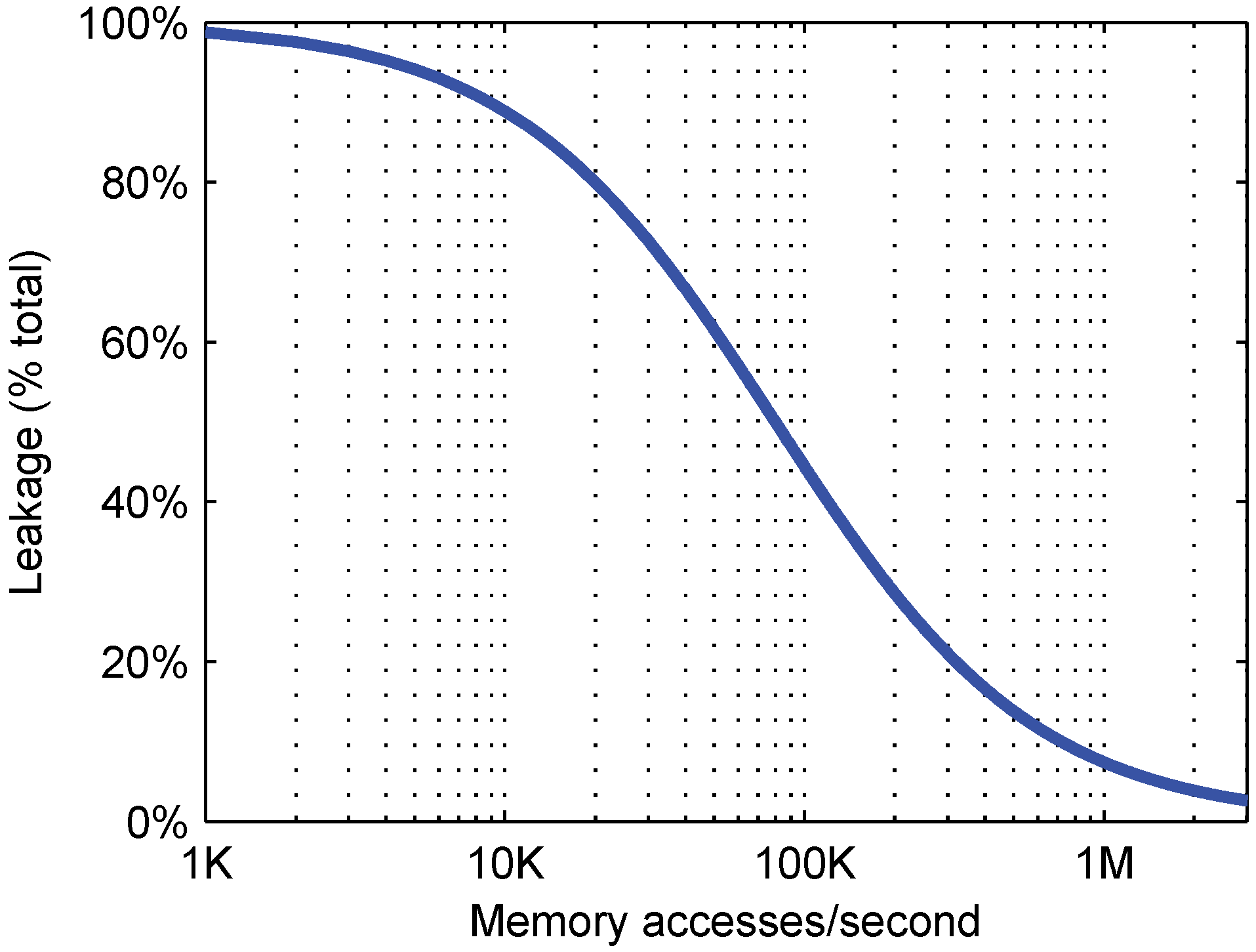
Figure 1. Leakage power divided by total memory power for different access rates. Data is generated using CACTI (a cache and memory access time model) 5.3 for 65-nm memories optimized for low standby current [16].
Jlpea 04 00231 g001
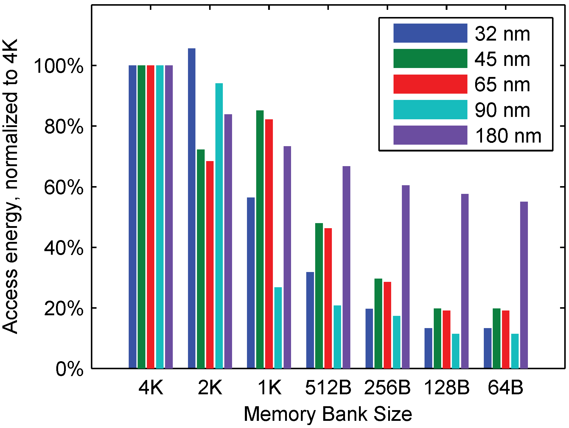
Figure 2. Access energies of low standby power memories of different sizes in different process technologies. Data is generated using CACTI and is based on ITRS (the International Technology Roadmap for Semiconductors) 2005 projections.
Jlpea 04 00231 g002
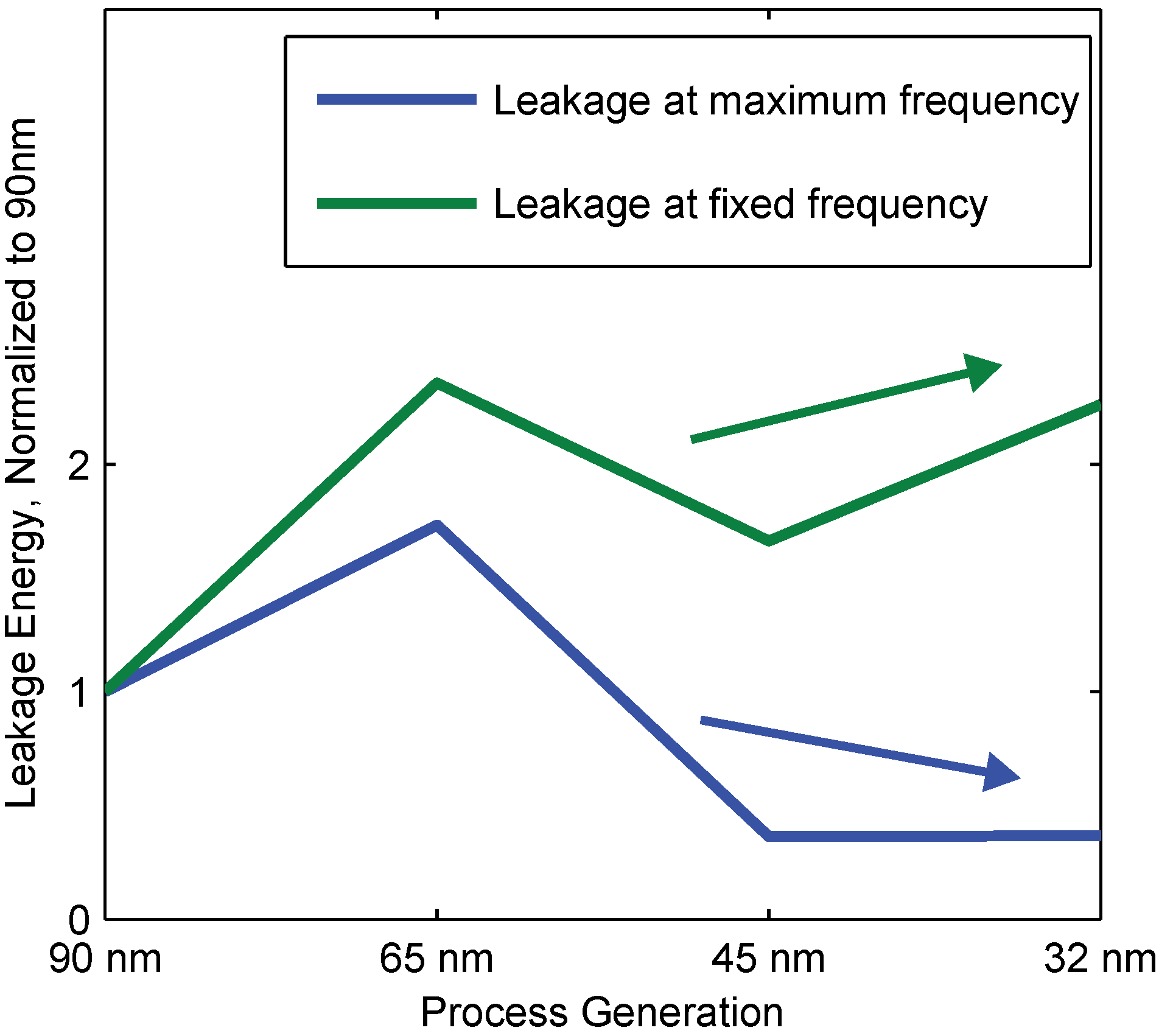
Figure 3. Leakage energy per access cycle for different processes with the maximum number of memory accesses for the process (blue) and a fixed number of memory accesses per second lower than the maximum frequency of any of the examined processes (green). Arrows indicate the general scaling trend of each type of application.
Jlpea 04 00231 g003

4.2. Relative Importance of Active and Leakage Energy

A small memory, such as a scratchpad memory, will usually have lower access energy than a large memory, like the main memory. On the other hand, the addition of a scratchpad memory will increase memory leakage power. If the scratchpad memory is used to reduce power, the reduction in access energy must outweigh the increase in leakage power. The scratchpad memory is usually very small compared to the main memory, so the increase in leakage power is generally very small, as well, but may be larger in future processes [11,17]. The relative importance of the access energy compared to the leakage energy depends on how frequently the memory is accessed in a given application. This concept is illustrated by Figure 1, which uses data from CACTI 5.3 to show leakage power as a percentage of total power for a given number of memory accesses per second. This figure demonstrates that for applications that rarely access the memory, leakage energy can dominate the memory’s energy consumption, and the additional leakage energy due to the scratchpad memory can be more significant than its access energy savings.

4.3. Access Energy and Memory Size

The benefit of the scratchpad memory, in terms of active energy reduction, is determined by the difference between S F E and M F E . Therefore, a key assumption of scratchpad memories is that small memories have lower access energies than large memories. To verify this assumption, access energy data was collected from CACTI cache simulations: an older version of CACTI [18] for 180 nm and CACTI 5.3 [16] for 90, 65, 45 and 32 nm. CACTI 5.3 uses technology information projected from the 2005 ITRS [16,17]. CACTI projections are based on a real physical layout, which includes detailed device and wire models. Even if device characteristics change over time, if the layout structures are similar, the trend of smaller memories consuming less power should be consistent. The data from CACTI 5.3 are more reliable than from the older version of CACTI, because its models are more closely derived from real physical structures. The normalized access energies of 64 B to 4 KB low standby power memories for these processes are shown in Figure 2. The simulated measurements show that access energy generally decreases with memory size in all of the simulated processes. There are a few exceptions to this rule, because CACTI simulates real layouts for memories that are primarily optimized for area and latency, rather than access energy. However, the general rule that access energy decreases with memory size is expected to hold, because larger memories will usually have longer wires and higher switching capacitance than small memories, so access energy is expected to decrease with memory size in all processes.

4.4. Leakage Energy and Process Scaling

An increase in total leakage current is the primary drawback of a scratchpad memory, so it is important to evaluate how scaling affects leakage energy to predict how beneficial scratchpad memories will be in future processes. The evaluation of leakage energy scaling trends depends on how often a memory will be accessed for a particular application. The higher frequencies enabled by newer processes help to decrease leakage energy per clock cycle, because the clock cycles are shorter, but if an application only requires a fixed number of memory accesses per second (lower than the maximum number of accesses), then the maximum speed of the memory is irrelevant. An application that accesses memory fewer times per second than the maximum possible frequency might be equivalently viewed as having a fixed memory access frequency lower than the maximum. The leakage trend for such an application running at a frequency fixed across process generations (and below the maximum of any of those processes) is contrasted to a memory running at maximum frequency of each process in Figure 3. The trend for an application with a frequency that is fixed across process generations does not improve as much with process scaling as an application that takes advantage of the maximum process frequency.
The purpose of Figure 3 is only to demonstrate the concept that leakage trends for fixed frequency applications are worse than trends for applications running at maximum frequencies if the newer processes target higher frequencies. Figure 3 is not intended to project specific leakage trends, because the 65-nm and later nodes had not yet been released when the source of its data, the 2005 ITRS, was published. A better description of recent leakage trends will be made in Section 5 using more recently published foundry process reports on transistor characteristics. The CACTI simulator used to generate Figure 3 has not yet been updated using the newest transistor data, so leakage trends must be projected using transistor data instead of simulations of memories.

5. Scaling Trends

Processes developed specifically for SoC applications have lower-power transistors and a larger variety of process options. Because embedded systems that are likely to benefit from a scratchpad memory are also likely to be built into these processes, these are the processes whose transistor characteristics should be examined.
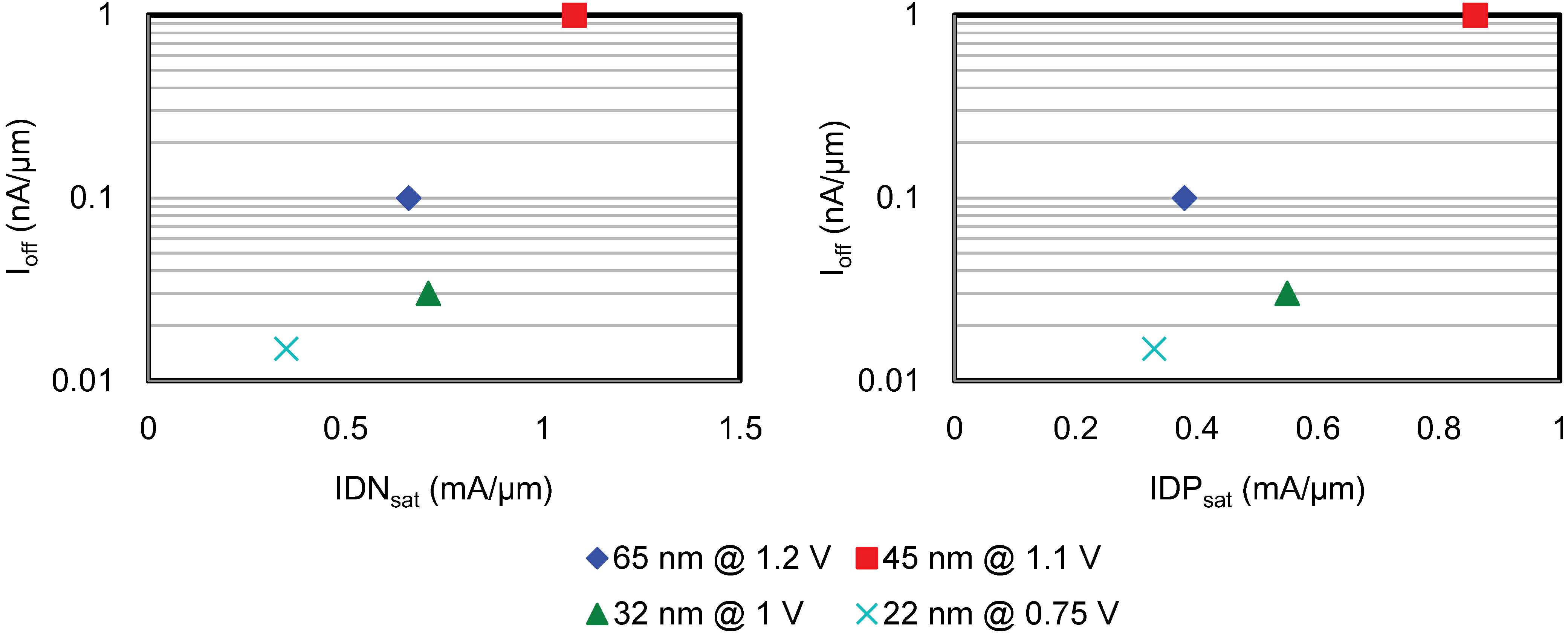
For simplicity, only Intel’s processes will be presented. Similar figures could be created for other foundries with low-power SoC processes, but the results would be similar. Figure 4 shows the reported achieved I D s a t and I o f f characteristics for the minimum channel length of the lowest available power type of both NMOS and PMOS transistors in Intel’s 65-, 45-, 32- and 22-nm low-power processes [19,20,21,22]. These are low-power SoC variants of high-performance processes. The 65-nm node was Intel’s first process node to introduce an SoC process. The I D s a t parameter reflects the drive strength of the transistor: larger I o n corresponds to a faster, higher-performance transistor in saturation; lower I o f f corresponds to a less leaky, more power-efficient transistor. The standard input voltages have decreased over time to decrease power consumption.
Figure 4. NMOS (left) and PMOS (right) reported drive currents and off-state leakages for minimum-length transistors of the lowest available power type available in each of Intel’s 65-, 45- and 32-nm SoC processes [19,20,21,22]. ID sat is the saturation drain current, or the current a transistor can provide when it is fully on. I off is the leakage current that is present when a transistor is turned off.
Jlpea 04 00231 g004
The overall trends illustrated in Figure 4 show that leakage has decreased over time. This decrease can be attributed to many process innovations, which will be examined in detail.

5.1. Process Innovations

Constant field scaling [23] has not been followed faithfully, but over recent process generations, voltages have been reduced. The last several process generations have employed a variety of innovative techniques to improve performance, while reducing leakage. An examination of the variety of process innovations that have driven improvement over the last several process generations indicates that future processes may also improve performance and reduce leakage through further innovations.
Contrary to constant field scaling rules, Intel’s 65-nm SoC process increased gate oxide thickness to decrease gate leakage. The good doping profile and source/drain spacers were optimized to prevent an increase in source-drain leakage, but this also increased the threshold voltage and decreased performance. The performance decrease was mitigated by uni-axial strained silicon [19].
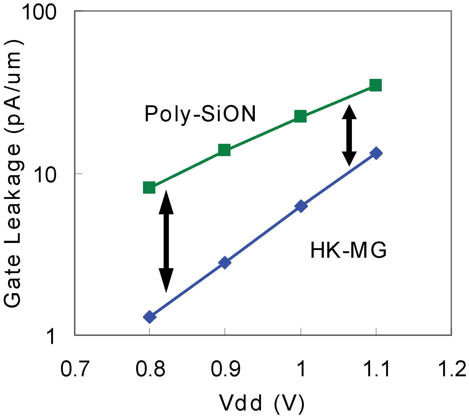
The 45-nm SoC process introduced a dramatic structural change: a Hafnium-based high-K metal gate (HKMG), which increased performance and decreased gate leakage by allowing for a physically thicker gate with the equivalent capacitance of a thin gate. Figure 5 shows how dramatically an HKMG can reduce gate leakage. However, gate leakage is still much less than source-drain leakage, and Figure 4 indicates that although the HKMG was introduced at the 45-nm node; total I o f f dropped much more significantly at the 32-nm node. The 32-nm node also utilized the HKMG and was the first Intel process node to use immersion lithography for the critical layer, allowing for resolution enhancement of that layer [20,21].
Figure 5. The addition of a high-K metal gate decreases leakage across all voltages in an IBM 32-nm process. Taken with permission from [24].
Jlpea 04 00231 g005
Intel’s 22-nm process introduced a significant advancement in process technology: a tri-gate transistor, also known as a FinFET. These transistors have a much steeper subthreshold slope than the planar 32-nm transistors [22]. This steeper subthreshold slope could be used to either significantly reduce leakage energy or to target a lower threshold voltage to increase performance. As with strained silicon and HKMG innovations, as the tri-gate transistor structure is refined, its impact will increase over time.
Research indicates that these transistor improvements are carrying over to SRAM improvements. For example, in the 22-nm technology, Intel created a low standby power SRAM with only 10-pA/cell standby leakages [22].
Other foundries have proposed other innovations for transistor structures that are targeted at reducing leakage energy, such as partially or fully-depleted SOI (silicon on insulator) or SuVolta’s deeply depleted channel (DDC) transistor [25]. In new process technologies, the improvements to energy savings and performance are now as much a result of structural redesign and innovation as they are of device dimension and voltage scaling.

5.2. SRAM Cell Design

Even if the process trends do not continue to reduce leakage power, as predicted in the previous section, SRAM cell design can be modified to reduce leakage. The traditional six-transistor (6T) bit cell suffers from low noise margins, so 8T-, 9T- and 10T-bit cells have been proposed to increase noise margins and enable lower supply voltages than are possible with the 6T cell. Because 8T- or 9T-bit cells can operate at lower voltages, the increased leakage energy due to higher transistor counts is offset by the decrease in leakage per transistor. Increased noise margins can enable higher threshold transistors to be used to reduce leakage [26]. 9T and 10T cells have achieved very low leakage levels at very low voltages [27,28]. The potential for implementing these design innovations further increases our confidence that leakage energy will not come to dominate power consumption to such an extent that the increased leakage of a scratchpad memory overwhelms its dynamic power savings for the foreseeable future.

6. WIMS Microcontroller

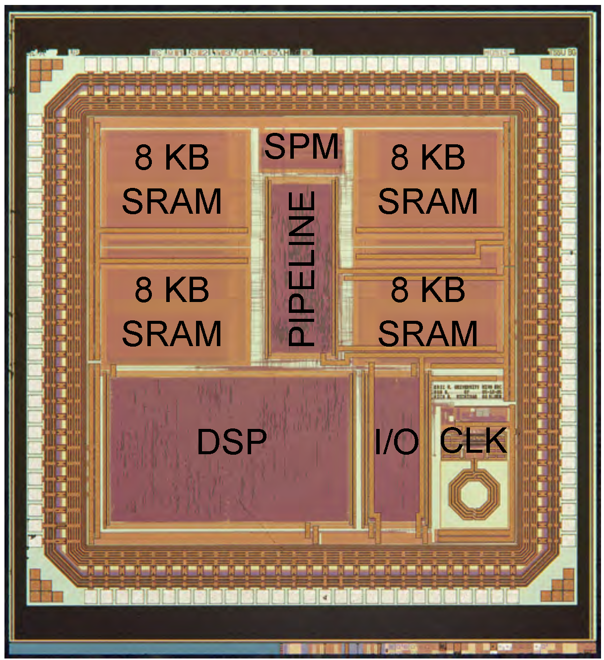
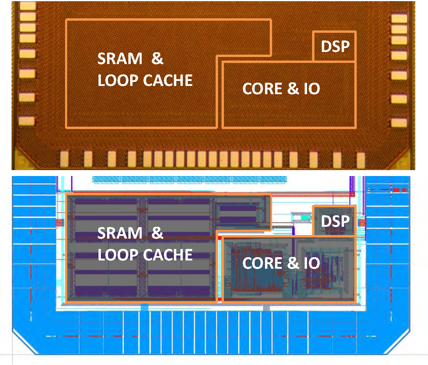
The WIMS microcontroller has been implemented in both 180- and 65-nm processes [2,29], as depicted in Figure 6 and Figure 7, with a small scratchpad memory to augment the on-chip main memory banks. Because it has had relatively few architectural changes between generations, it is a good test bed for evaluating the advantages of scratchpad memories as processes are scaled. Measured data from both implementations will be used to investigate the implications of process differences on the energy savings available from small scratchpad memories, and Intel’s transistor data will be used to project energy savings for a hypothetical 32-nm version of the microcontroller.
The WIMS microcontroller is designed for low-power embedded applications, such as environment and health monitoring. Its scratchpad memory is 1 KB. This memory is entirely software-controlled, but is managed in much the same way as a loop cache by the WIMS compiler. The microcontroller has a three-stage pipeline and runs at more than 200 MHz; the maximum frequency is unknown due to tester limitations. Its on-chip main memory is 32 KB, composed of four 8-KB banks.
Although the scratchpad memory in the WIMS microcontroller was originally referred to as a loop cache [10], it will be referred to as a scratchpad memory here to be consistent with conventional terminology [9], because it does not have a hardware controller or tag comparison circuitry. Unlike a typical cache or a hardware-controlled loop cache, the scratchpad is memory-mapped, so that it can be managed by the compiler.
Figure 6. A die photo of the 180-nm WIMS microcontroller.
Jlpea 04 00231 g006
Figure 7. The layout of the third-generation WIMS microcontroller. The die photo on top shows metallization with block outlines added. The lower image is a screenshot of the digital logic layout.
Jlpea 04 00231 g007

6.1. Measured Data

Measurements from the 65-nm WIMS microcontroller were recorded at the University of Utah using the Verigy 93000 PS400 SOC tester. The memories are in a separate power domain, so that their power consumption could be easily separated from that of the core. To estimate energy savings, three variables were measured: main memory fetch energy ( M F E ), scratchpad fetch energy ( S F E ) and leakage energy ( L E ). Scratchpad leakage energy ( S L E ) was estimated by using memory compiler reports for a commercial 65-nm memory compiler. The memory compiler reports estimate the leakage power of the memory and showed that S L E is approximately 3% of L E , while the main memory leakage energy ( M L E ) is 97% of L E . This result is intuitive, because the scratchpad memory is approximately 3% of the system memory. To measure M F E and S F E , a loop of code was executed from main memory and subsequently from scratchpad memory, and memory power was measured while running at various frequencies and voltages. The static memory power draw was also measured for each voltage. The power draw was divided by the clock cycle to find the energy consumed per clock cycle. M F E and S F E were found by subtracting L E from the energy measured during execution from the main memory and scratchpad memory, respectively.
Energy savings were then calculated using (2), but simplified by setting A R to one, because the entire program was placed in the scratchpad memory:
1 - E S = S F E + M L E + S L E M F E + M L E
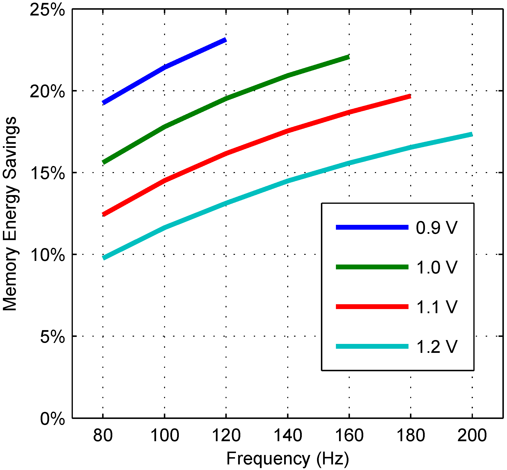
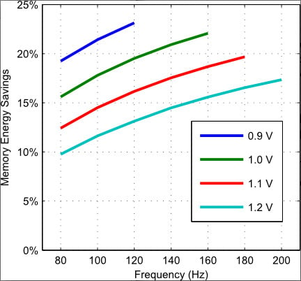
The percentage of energy saved using the scratchpad memory versus main memory in the 65-nm WIMS microcontroller implementation is depicted in Figure 8 for voltages between 0.9 and 1.2 V and frequencies between 80 and 200 MHz. As explained above, the total energy includes leakage energy. The scratchpad memory saves 10%–25% of total energy across all measurements, with the maximum savings achieved at the lowest voltages. These large total energy savings justify the use of a scratchpad memory in any application that has frequently used code or data and where dynamic power is a major contributor to total power.
Figure 8. Measured memory energy savings from executing code from the scratchpad memory instead of the main memory on the 65-nm WIMS microcontroller.
Jlpea 04 00231 g008
Even in efficient operating regimes, using the lowest possible supply voltage for a given clock frequency, leakage is responsible for approximately 45% of the total energy for the 65-nm WIMS microcontroller. This relatively high leakage ratio limits the total energy savings, because the scratchpad memory can only reduce dynamic energy consumption.

6.2. 32-nm Projections

To investigate whether recent scaling trends are advantageous or detrimental to scratchpad memories, the energy savings of a hypothetical 32-nm version of the WIMS microcontroller are projected. The 32-nm process was selected instead of the 22-nm process, because the 32-nm process is planar, so the assumptions necessary for the projection are more justifiable. To project the values of S F E , M F E , S L E and M L E that would likely be attained by a 32-nm version of the WIMS microcontroller, the energy measurements from the 65-nm version are scaled according to the transistor trends depicted in Figure 4. First, transistor parameters must be related to the energy variables in (4). Leakage energy per clock period ( L E ) is proportional to the supply voltage (V) multiplied by the leakage current ( I l e a k ) and the clock period ( t f ):
L E V · I l e a k · t f
Leakage current can be further broken down into leakage per micron of gate width ( I l e a k / µm) multiplied by the average gate width ( G W ):
L E V · I l e a k µm · G W · t f
Because the scratchpad memory primarily saves active energy, at the expense of a small increase in leakage energy, projected results are conservative if the decrease in leakage is underestimated and the decrease in active energy is overestimated. Based on the data presented in Figure 4, I l e a k / µm in 32 nm is 30% of its value in the 65-nm process, while the voltage is reduced from 1.2 V to 1.0 V. To keep results conservative, no reduction in clock period was assumed. Therefore, in a 32-nm process, L E / G W , relative to the 65-nm process, is approximately:
L E 32 / G W 32 L E 65 / G W 65 = I l e a k 32 / µm I l e a k 65 / µm · V 32 V 65 = 0.3 · 1.0 V 1.2 V = 0.25
where the “32” and “65” subscripts indicate whether the parameters are for 32 nm or 65 nm, respectively. To estimate G W 32 / G W 65 , it is assumed that the reduction in gate area ( A 32 / A 65 ) is approximately the same as the reduction in bit cell area. For the lowest power option, minimum G L is 55 nm in Intel’s 65-nm technology and 46 nm in Intel’s 32-nm technology. The bit cell area decreased from 0.68 µm2 in 65 nm to 0.171 µm2 in 32 nm (to 25% of its original value) [19,21]. Therefore,
G W 32 G W 65 = A 32 A 65 · G L 65 G L 32 = 0.171 µm 2 0.68 µm 2 · 55 nm 46 nm = 0.3
In sum, L E in 32 nm, relative to 65 nm, is estimated to be:
L E 32 L E 65 = L E 32 / G W 32 L E 65 / G W 65 · G W 32 G W 65 = 0.25 · 0.3 = 0.075
Now that the leakage scaling ratio has been found, the fetch energy scaling ratio will be considered. The fetch energy ( F E ) is assumed to be proportional to dynamic switching energy, which is proportional to the switching capacitance of the wires and transistors (C) times the supply voltage (V) squared:
F E C · V 2 = ( C t + C w ) · V 2
where C t represents capacitance due to transistors and C w represents the capacitance due to wires. First, the division between wire capacitance and transistor capacitance should be estimated for our SRAM. This division was studied for wires of different lengths in a 130-nm process [30]. This study can be used to indicate the division between C w and C t if the WIMS microcontroller SRAM’s wire lengths can be estimated and then converted to the 130-nm equivalent. The 65-nm WIMS SRAM uses 8-KB banks, each of which are 320 µm × 170 µm . Its wires are therefore up to 320 µm, and these lengths should be doubled to up to 640 µm to be equivalent to a 130-nm process. Magen et al. [30] indicates that for wires up to 640 µm long, C w is approximately 40% of total C.
C t can be estimated by assuming that C t is roughly proportional to the gate area of the transistor and that the decrease in the gate area of the transistor is proportional to the decrease in the area of one SRAM bit cell. This last assumption was also made by (8). The decrease in the SRAM bit cell area is from 0.68 µm2 in 65 nm to 0.171 µm2 in 32 nm. Therefore,
C t 32 C t 65 = 0.171 µm 2 0.68 µm 2 = 0.25
To estimate C w 32 / C w 65 , the predictive technology model was used to find the wire capacitance in the 65-nm process [31], and 2011 ITRS parameters were used to estimate the wire capacitance in the 32-nm process [32]. Using the typical wire dimensions suggested by the predictive technology model, a typical wire in 65-nm has about 1.46 pF/cm of capacitance. Table INTC2 in the Interconnect section of the 2011 ITRS lists intermediate wires having 1.8 pF/cm of capacitance in 2011, the year the 32-nm node was introduced. This is a slight increase, but the length of each wire is halved, so the total change in C w is:
C w 32 C w 65 = 0.5 · 1 . 8 pF cm 1 . 46 pF cm = 0.62
Although the scaling of the wire capacitance is worse than transistor capacitance scaling, this poor scaling actually makes scratchpad memories more attractive, because it increases dynamic power (which scratchpad memories reduce) relative to leakage power. Now, it is possible to find the overall capacitance scaling:
C 32 C 65 = C t 32 + C w 32 C 65 = C t 32 C 65 + C w 32 C 65 = C t 65 C 65 · C t 32 C t 65 + C w 65 C 65 · C w 32 C w 65 = 0.6 · 0.25 + 0.4 · 0.62 = 0.398
F E 32 / F E 65 can be calculated using (10):
F E 32 F E 65 = C 32 C 65 · V 32 V 65 2 = 0.398 · 1.0 V 1.2 V 2 = 0.276
Using these scaling figures for L E and F E , the energy savings of the WIMS scratchpad memory will be projected for 32 nm, based on the 65-nm measured data.

6.3. WIMS Scratchpad Memory Approach

The WIMS scratchpad memory is compiler-controlled. When use of the scratchpad memory was analyzed [10], two compiler management methods were implemented: “static” and “dynamic.” The static method identifies the most frequently used loops and data objects and places as many as fit into the scratchpad memory for the duration of the program execution. The dynamic method uses a trace-selection algorithm to determine whether the energy savings of having a certain program loop in the scratchpad memory is worth the energy of copying it into the scratchpad. Copy instructions are then inserted in the program to ensure that the selected loop or data is copied to the scratchpad memory before it is executed or accessed.
The example program depicted in Figure 9 will be used to illustrate the differences between the static and dynamic methods, after each algorithm is summarized. The compiler routine for the static allocation algorithm can be summarized as follows:
  • Identify the most executed blocks of code.
  • Assign these blocks of code, in the order of the most used first, to the scratchpad memory, until it is full.
  • Redirect instruction fetch (when entering code block), subroutine calls and references to these blocks to the new locations in the scratchpad memory.
Figure 9. An example program in which each numbered block represents a piece of code and an arrow represents a possible execution path. The boxes shaded the darkest are the most frequently executed. The static allocation method will hold Blocks 4 and 5 in the scratchpad memory for the duration of the execution of the program, whereas the dynamic allocation method will replace those blocks with Blocks 10 and 11 prior to their execution.
Jlpea 04 00231 g009
In the example program in Figure 9, the loop consisting of Blocks 4 and 5 is the most frequently executed code in the program, followed by the loop consisting of Blocks 10 and 11. If only two blocks can fit in the scratchpad memory, then the static method will place Blocks 4 and 5 in the scratchpad memory for the duration of the execution of the program.
In the dynamic method, the compiler uses profiling to determine how much energy would be saved by moving a block to the scratchpad memory. If the compiler determines that the energy saved by running a block from the scratchpad memory is worth the energy of copying the code to the scratchpad memory, then it will assign those code blocks to addresses in the scratchpad memory. The dynamic allocation algorithm can be summarized as:
  • Identify blocks of code, such that the energy to copy the code to the scratchpad memory is less than the energy saved by executing the code from the scratchpad memory.
  • Assign these blocks of code addresses in the scratchpad memory and redirect references to them to their new addresses.
  • Insert copy instructions immediately prior to each of these blocks, so that the block will be in the scratchpad memory prior to its execution or prior to its being called if it is a subroutine.
  • Consolidate copy instructions to avoid unnecessary copying.
In the example program in Figure 9, if the compiler determines that the energy savings of running Blocks 4, 5, 10 and 11 is worth copying them to the scratchpad memory, then each block will be placed in the scratchpad memory and instructions will be inserted to copy each block to the scratchpad memory prior to its execution. Assuming two blocks can fit in the scratchpad memory, the copy instructions for Blocks 4 and 5 will be consolidated, as well as the copy instructions for Blocks 10 and 11.
The compiler uses execution profile information and an energy benefit heuristic to determine which blocks to move to the scratchpad memory. Details of the compilation procedures used in the static and dynamic allocation methods are beyond the scope of this paper, but are available in [10].
The energy savings of the dynamic and static methods will be presented for the 180- and 65-nm processes based on measured data, and the energy savings of a hypothetical 32-nm process will be projected.

6.4. Static Benchmarks

The benchmarks used to compare the scratchpad memory energy savings in the 180-, 65- and 32-nm processes are the same as those used to compare the static and dynamic allocation methods in [10]. Those benchmarks are a subset of the MediaBench [33] and MiBench [34] benchmarks, oriented towards embedded systems. This selection of benchmarks is convenient, because scratchpad memory access rates for each of these benchmarks have already been published in [10] for the WIMS microcontroller, using the static allocation method. This data can be used to project the energy savings ( E S ) of the microcontroller using the model represented by (2), repeated here with a slight modification for convenience:
1 - E S = A R · S F E + ( 1 - A R ) · M F E + L E M F E + M L E
Leakage energy ( L E ) has replaced M L E + S L E for brevity ( L E = M L E + S L E ). The access rates ( A R ) are found in [10]. S F E , M F E and L E were measured for 0.9 V and 120 MHz, as described in Section 6.1, and M L E = 0.97 · L E , as noted in the same section. The frequency of 120 MHz was selected, because it was the highest operational frequency for the microcontroller with a 0.9-V supply voltage. Projected energy savings are presented in Figure 10 for a 256 B scratchpad memory. The 65-nm WIMS microcontroller has a larger 1 KB scratchpad memory, but scratchpad access rates were not available for all benchmarks for that larger size, so the results presented are conservative. The 32-nm projections of each of these variables were made using the method described in Section 6.2.
Figure 10. Comparison of energy savings from a scratchpad memory in 180-, 65- and 32-nm technologies, using the static allocation method.
Jlpea 04 00231 g010
The scratchpad memory is limited to saving dynamic power, which is only ~55% of the WIMS microcontroller’s total memory power. The remaining ~45% is due to leakage. Thus, despite savings as high as 40% in terms of dynamic energy consumption, Figure 10 shows lower total energy savings because of the high leakage power.

6.5. Dynamic Benchmarks

To use the measured data to project energy savings from using the dynamic allocation scheme, two new variables are added to the model:
1 - E S = A R · S F E + ( 1 - A R ) · M F E + C O · ( M F E + S W E ) + L E M F E + M L E
C O (copy overhead ratio) represents the impact of the additional instructions necessary to copy code from the main memory to the scratchpad memory during execution, per memory access. Because a copy involves a read from main memory and a write to scratchpad memory, C O is proportional to M F E and S W E (scratchpad write energy). For the 180-nm processor, all of these variables are reported for each benchmark except for C O , which was solved for using Equation (16).
For the 65-nm processor and 32-nm projection, the copy overhead ratio C O is the same as it is in the 180-nm processor, because the memory sizes and ISA (instruction set architecture) are the same, so the number of copy instructions executed to fill the scratchpad during execution will be the same. S F E was substituted for S W E , because the available S F E data were more reliable. Tests on the 180-nm processor indicated that the read and write energies are similar; specifically, the read and write energies of a 512 B memory were virtually identical, and the read and write energies of a 1 KB memory (the size of the scratchpad on the WIMS microcontroller) were within 20% of each other. E S was then calculated for the 65-nm processor using (16). The 32-nm projections were again made using the method described in Section 6.2.
The results depicted in Figure 10 and Figure 11 reveal that: (1) the dynamic allocation method generally increases the energy savings achieved by the scratchpad memory; (2) the scratchpad memory saves substantial energy in every examined process; and (3) that energy savings expected in a 32-nm version of the microcontroller should be even greater than observed in the 65-nm version.
Figure 11. Comparison of energy savings from a scratchpad memory in 180-, 65- and 32-nm technologies, using the dynamic allocation method.
Jlpea 04 00231 g011

7. Conclusions

Despite the high leakage ratio at the 65-nm process node, this study has shown that the energy saved by using scratchpad memories continues to merit their consideration. In nodes with lower leakage ratios, such as the 45- or 32-nm nodes, or with memories that are optimized to minimize leakage power, scratchpad memories are even more attractive. In particular, the largest gains were found for frequent memory accesses and minimal memory supply voltage. Although this study focused on using scratchpad memories for instruction storage, we believe these conclusions will hold if the scratchpad memories are used for data storage, as well. Applications with low memory-access frequency or that use processes with high leakage-to-dynamic power ratios will see limited savings from scratchpad memories. These conclusions were supported by data measured from the WIMS microcontroller implemented in both 180- and 65-nm processes. CACTI simulations were used to demonstrate how process characteristics impact SRAM energy consumption and scratchpad memory energy savings. Intel process technology reports indicate that process innovations will continue to decrease leakage energy. These data can guide the design process at multiple levels from software to architecture to process selection. In many applications, scratchpad memories will provide significant savings in dynamic power consumption at little cost in leakage power, even in advanced semiconductor processes. This power savings is likely to continue for the process nodes of the foreseeable future.

Acknowledgments

This work was supported by the Engineering Research Center Program of the National Science Foundation under Award No. EEC-9986866. This work made use of University of Utah Shared Facilities supported, in part, by the MRSEC (Materials Research Science and Engineering Centers) Program of the NSF under Award No. DMR-1121252. Chip testing was enabled by the use of VTRAN (a vector translation program) from the kind support of Source III. Chip fabrication was made possible by MOSIS (Metal Oxide Semiconductor Implementation Service, an organization that provides multi-project wafers). Toren Monson assisted in the testing of the 65-nm WIMS microcontroller.

Author Contributions

Bennion Redd wrote the first drafts of the text and incorporated the other authors’ feedback, as well as led the testing of the 65-nm WIMS microcontroller on the Verigy 93000. Spencer Kellis and Nathaniel Gaskin led the tape-out process to prepare the chip design for fabrication at MOSIS, and Richard Brown supported and directed work on the WIMS microcontroller, consulted on design decisions, suggested research ideas and offered valuable feedback on revisions of the paper.

Conflicts of Interest

The authors declare no conflict of interest.

References

  1. Redd, B.; Kellis, S.; Gaskin, N.; Brown, R. Scratchpad Memories in the Context of Process Scaling. In Proceedings of the IEEE 54th International Midwest Symposium on the Circuits and Systems (MWSCAS), Seoul, Korea, 7–10 August 2011.
  2. Kellis, S.; Gaskin, N.; Redd, B.; Campbell, J.; Brown, R. Energy Profile of a Microcontroller for Neural Prosthetic Application. In Proceedings of the IEEE International Symposium on Circuits and Systems, Paris, France, 30 May–2 June 2010; pp. 3841–3844.
  3. Steinke, S.; Wehmeyer, L.; Bo-Sik, L.; Marwedel, P. Assigning Program and Data Objects to Scratchpad for Energy reduction. In Proceedings of the Design, Automation and Test in Europe Conference and Exhibition, Paris, France, 4–8 March 2002; pp. 409–415.
  4. Kin, J.; Gupta, M.; Mangione-Smith, W.H. The Filter Cache: An Energy Efficient Memory Structure. In Proceedings of the 30th Annual ACM/IEEE International Symposium Microarchitecture, Washington, DC, USA, 1–3 December 1997; pp. 184–193.
  5. Bellas, N.; Hajj, I.; Polychronopoulos, C.; Stamoulis, G. Energy and Performance Improvements in Microprocessor Design Using a Loop Cache. In Proceedings of the International Conference on Computer Design (ICCD ’99), Austin, TX, USA, 10–13 October 1999; pp. 378–383.
  6. Lea Hwang, L.; Moyer, B.; Arends, J. Instruction Fetch Energy Reduction Using Loop Caches for Embedded Applications with Small Tight Loops. In Proceedings of the Low Power Electronics and Design, San Diego, CA, USA, 17 August 1999; pp. 267–269.
  7. Gordon-Ross, A.; Cotterell, S.; Vahid, F. Exploiting fixed programs in embedded systems: A loop cache example. IEEE Comp. Archit. Lett. 2002, 1, 2. [Google Scholar] [CrossRef]
  8. Egger, B.; Lee, J.; Shin, H. Scratchpad Memory Management for Portable Systems with a Memory Management Unit. In Proceedings of the 6th ACM & IEEE International Conference on Embedded Software (EMSOFT ’06), Seoul, Korea, 22–25 October 2006; ACM: New York, NY, USA, 2006; pp. 321–330. [Google Scholar]
  9. Verma, M.; Wehmeyer, L.; Marwedel, P. Cache-Aware Scratchpad Allocation Algorithm. In Proceedings of the Design, Automation and Test in Europe Conference and Exhibition, Washington, DC, USA, 16–20 February 2004; pp. 1264–1269.
  10. Ravindran, R.A.; Nagarkar, P.D.; Dasika, G.S.; Marsman, E.D.; Senger, R.M.; Mahlke, S.A.; Brown, R.B. Compiler Managed Dynamic Instruction Placement in a Low-Power Code cache. In Proceedings of the International Symposium on Code Generation and Optimization (CGO), Washington, DC, USA, 20–23 March 2005; pp. 179–190.
  11. Borkar, S. Design challenges of technology scaling. Micro IEEE 1999, 19, 23–29. [Google Scholar] [CrossRef]
  12. Guangyu, C.; Feihui, L.; Ozturk, O.; Guilin, C.; Kandemir, M.; Kolcu, I. Leakage-Aware SPM Management. In Proceedings of the IEEE Computer Society Annual Symposium on Emerging VLSI Technologies and Architectures, Karlsruhe, Germany, 2–3 March 2006.
  13. Kandemir, M.; Irwin, M.J.; Chen, G.; Kolcu, I. Compiler-guided leakage optimization for banked scratch-pad memories. IEEE Trans. Larg. Scale Integr. (VLSI) Syst. 2005, 13, 1136–1146. [Google Scholar] [CrossRef]
  14. Huangfu, Y.; Zhang, W. Compiler-based approach to reducing leakage energy of instruction scratch-pad memories. In Proceedings of the 2013 IEEE 31st International Conference on Computer Design (ICCD), Asheville, NC, USA, 6–9 October 2013; pp. 439–442.
  15. Takase, H.; Tomiyama, H.; Zeng, G.; Takada, H. Energy efficiency of scratch-pad memory in deep submicron domains: An empirical study. IEICE Electron. Express 2008, 5, 1010–1016. [Google Scholar] [CrossRef]
  16. Thoziyoor, S.; Muralimanohar, N.; Ahn, J.; Jouppi, N. CACTI 5.1. Available online: http://www.hpl.hp.com/techreports/2008/HPL-2008-20.html (accessed on 5 June 2014).
  17. 2005 International Technology Roadmap for Semiconductors. Available online: http://www.itrs.net/reports.html (accessed on 5 June 2014).
  18. Wilton, S.; Jouppi, N. CACTI: An enhanced cache access and cycle time model. IEEE J. Solid-State Circuits 1996, 31, 677–688. [Google Scholar] [CrossRef]
  19. Jan, C.H.; Bai, P.; Choi, J.; Curello, G.; Jacobs, S.; Jeong, J.; Johnson, K.; Jones, D.; Klopcic, S.; Lin, J.; et al. A 65 nm Ultra Low Power Logic Platform Technology Using Uni-Axially Strained-Silicon Transistors. In Proceedings of the 2005 IEEE International Electron Devices Meeting (IEDM) Technical Digest, Washington, DC, USA, 5 December 2005; pp. 60–63.
  20. Jan, C.H.; Bai, P.; Biswas, S.; Buehler, M.; Chen, Z.P.; Curello, G.; Gannavaram, S.; Hafez, W.; He, J.; Hicks, J.; et al. A 45 nm Low Power System-on-Chip Technology with Dual Gate (Logic and I/O) High-k/Metal Gate Strained Silicon Transistors. In Proceedings of the 2008 IEEE International Electron Devices Meeting (IEDM 2008), San Francisco, CA, USA, 15–17 December 2008.
  21. Jan, C.H.; Agostinelli, M.; Buehler, M.; Chen, Z.P.; Choi, S.J.; Curello, G.; Deshpande, H.; Gannavaram, S.; Hafez, W.; Jalan, U.; et al. A 32 nm SoC Platform Technology with 2nd Generation High-k/Metal Gate Transistors Optimized for Ultra Low Power, High Performance, and High Density Product Applications. In Proceedings of the 2009 IEEE International Electron Devices Meeting (IEDM), Baltimore, MD, USA, 7–9 December 2009.
  22. Jan, C.H.; Bhattacharya, U.; Brain, R.; Choi, S.J.; Curello, G.; Gupta, G.; Hafez, W.; Jang, M.; Kang, M.; Komeyli, K.; et al. A 22 nm SoC Platform Technology Featuring 3-D Tri-gate and High-k/metal gate, optimized for ultra low power, high performance and high density SoC applications. In Proceedings of the 2012 IEEE International Electron Devices Meeting (IEDM), San Francisco, CA, USA, 10–13 December 2012; pp. 3.1.1–3.1.4.
  23. Dennard, R.; Gaensslen, F.; Rideout, V.; Bassous, E.; LeBlanc, A. Design of ion-implanted MOSFET’s with very small physical dimensions. Solid-State Circuits IEEE J. 1974, 9, 256–268. [Google Scholar] [CrossRef]
  24. Yang, H.S.; Wong, R.; Hasumi, R.; Gao, Y.; Kim, N.S.; Lee, D.H.; Badrudduza, S.; Nair, D.; Ostermayr, M.; Kang, H.; et al. Scaling of 32 nm Low Power SRAM with High-K Metal Gate. In Proceedings of the 2008 IEEE International Electron Devices Meeting (IEDM), San Francisco, CA, USA, 15–17 December 2008.
  25. Fujita, K.; Torii, Y.; Hori, M.; Oh, J.; Shifren, L.; Ranade, P.; Nakagawa, M.; Okabe, K.; Miyake, T.; Ohkoshi, K.; et al. Advanced Channel Engineering Achieving Aggressive Reduction of VT Variation for Ultra-Low-Power Applications. In Proceedings of the 2011 IEEE International Electron Devices Meeting (IEDM), Washington, DC, USA, 5–7 December 2011; pp. 32.3.1–32.3.4.
  26. Athe, P.; Dasgupta, S. A Comparative Study of 6T, 8T and 9T Decanano SRAM Cell. In Proceedings of the 2009 IEEE International Symposium on Industrial Electronics Applications (ISIEA 2009), Kuala Lumpur, Malaysia, 4–6 October 2009; Volume 2, pp. 889–894.
  27. Calhoun, B.H.; Chandrakasan, A. A 256kb Sub-threshold SRAM in 65 nm CMOS. In Proceedings of the 2006 IEEE International Solid-State Circuits Conference Digest of Technical Papers (ISSCC 2006), San Francisco, CA, USA, 6–9 February 2006; pp. 2592–2601.
  28. Lin, S.; Kim, Y.B.; Lombardi, F. A Low Leakage 9T Sram Cell for Ultra-Low Power Operation. In Proceedings of the 18th ACM Great Lakes Symposium on VLSI, Orlando, FL, USA, 4–6 May 2008; ACM Press: New York, NY, USA, 2008; pp. 123–126. [Google Scholar]
  29. Marsman, E.; Senger, R.; McCorquodale, M. A 16-bit Low-Power Microcontroller with Monolithic MEMS-LC Clocking. In Proceedings of the 2005 IEEE International Symposium on Circuits and Systems (ISCAS 2005), Kobe, Japan; 2005; pp. 624–627. [Google Scholar]
  30. Magen, N.; Kolodny, A.; Weiser, U.; Shamir, N. Interconnect-Power Dissipation in a Microprocessor. In Proceedings of the 2004 International Workshop on System Level Interconnect Prediction (SLIP ’04), Paris, France, 14–15 February 2004; ACM: New York, NY, USA, 2004; pp. 7–13. [Google Scholar]
  31. Predictive Technology Model. Available online: http://ptm.asu.edu/interconnect.html (accessed on 5 June 2014).
  32. 2011 International Technology Roadmap for Semiconductors. Available online: http://www.itrs.net/reports.html (accessed on 5 June 2014).
  33. Lee, C.; Potkonjak, M.; Mangione-Smith, W. MediaBench: A Tool for Evaluating and Synthesizing Multimedia and Communications Systems. In Proceedings of the 30th Annual IEEE/ACM International Symposium on Microarchitecture, Research Triangle Park, NC, USA, 1–3 December 1997; pp. 330–335.
  34. Guthaus, M.; Ringenberg, J.; Ernst, D.; Austin, T.; Mudge, T.; Brown, R. MiBench: A Free, Commercially Representative Embedded Benchmark Suite. In Proceedings of the 2001 IEEE International Workshop on Workload Characterization (WWC-4 2001), Washington, DC, USA, 2 December 2001; pp. 3–14.