1. Introduction
Since 2007, our society has used more energy for browsing the Internet than for air travel [
1]. It is also predicted that the energy (and environmental) footprint of computation and data traffic will steadily increase in the near future: Data centres will grow and so will the network infrastructure together with the number of terminal nodes of the global information network such as computers, phones, gadgets and other connected cyber-physical devices (so called Internet of Things) [
1]. Energy-efficiency of components at all levels of the computation hierarchy is thus becoming a major concern for the microelectronics industry. A serious factor impeding the progress in addressing this concern is a wide gap between the ways of how energy efficiency is approached by hardware and software engineers, and this gap is emphasised by the lack of common understanding between the two communities.
In this paper we discuss an approach to bridging this gap by developing a shared design criterion, called
power-proportionality, on the basis of which both electronics and programming solutions can be judged. A computing system, for it to be considered power-proportional, has to keep power consumption and computation load proportional to each other. That is, an idle system would ideally consume no power, whereas given a small energy budget the system would adapt itself by reducing its computation flow and lowering the delivered Quality-of-Service (QoS), and still remain functional; see
Section 2 for a detailed discussion. The state-of-the-art systems have generally poor power-proportionality; for example, the servers used in data centres typically consume 50%–60% of peak power under 10% of peak load [
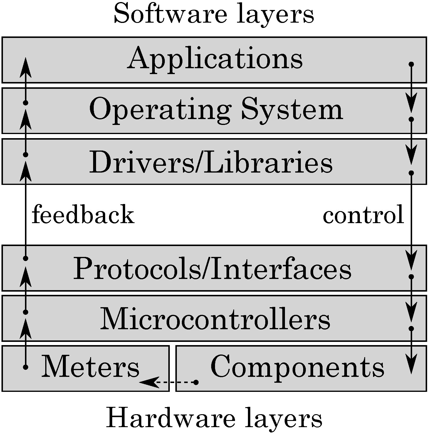
2]. We hypothesise that modern systems exhibit poor power proportionality because they are designed to operate in a narrow scope of conditions, typically optimised for either high performance or low power consumption. This approach is inherently flawed because all the design effort is focused on one particular operation mode disregarding others. Another issue that makes it difficult to handle unpredictable environmental conditions is the absence of a cross-layer feedback-control loop between energy supply components (in hardware) and an operating system or an active application (in software), see
Figure 1: software is unable to steer the computation with the aim of maximising QoS by prioritising tasks, trading accuracy for energy, and, in general, by strategic planning of energy resource utilisation.
Figure 1.
Cross-layer power proportionality.
Figure 1.
Cross-layer power proportionality.
In this paper we discuss cross-layer hardware-software mechanisms for online energy monitoring and reconfiguration. The particular focus is on methodology for design and implementation of power-proportional microprocessors, capable of adapting to varying operating conditions (such as low or even unstable voltage level) and application requirements in runtime. We use a popular Intel 8051 microprocessor as our running example to demonstrate the soundness of the approach. The obtained reconfigurable implementation compares favourably to existing specialised (non-reconfigurable) Intel 8051 designs. Our approach is different from conventional power optimisation techniques, such as [
3], because we extend the microarchitecture of the processor and allow its runtime reconfiguration, thereby facilitating the cross-layer feedback-control loop shown in
Figure 1.
The paper is organised as follows.
Section 2 discusses the challenges in design of reconfigurable processors and introduces the concept of power-proportional computing.
Section 3 gives a brief background on the Conditional Partial Order Graph (CPOG) model which we use for the specification and synthesis of processor microarchitectures. We then focus specifically on design of reconfigurable microarchitectures in
Section 4. This is followed by a case study on design and implementation of a reconfigurable and power-proportional version of the Intel 8051 core in
Section 5.
2. Reconfigurability and Power Proportionality
How can one build a reconfigurable and adaptable processor? The first thought could be to implement it in the
field-programmable gate array (FPGA) technology allowing static and, sometimes, dynamic reconfiguration. Such a processor would be capable of adjusting its internal structure or behaviour by rewiring interconnections between its components or even by changing functionality at the level of individual gates. This technology can provide a very fine-grain control over a system at runtime, however, the associated overheads are extremely high. In particular, in terms of energy consumption, FPGAs are typically 10–15 times more expensive than
application-specific integrated circuits (ASICs); see a collection of recent FGPA
vs. ASIC interviews with industrial experts in [
4].
Since the fine-grain reconfigurability offered by FPGAs is overly costly in the context of energy-constrained systems, one shall consider the coarse-grain reconfigurable architectures in the ASIC realm. They significantly lower the overheads by dropping reconfigurability in datapath components and utilising their custom designed versions instead. The control logic and interconnect fabric, however, retain the capability to reconfiguration. In this setting, the key design and implementation challenge is to formally describe and synthesise the controller whose task is to coordinate hard system resources (the datapath components and interconnects) according to the runtime information on availability of soft system resources (energy and time); the latter can also include information on hardware faults in a system, thereby allowing the controller to bypass faulty components whenever possible.
Figure 2 illustrates the concept of
power-proportionality and its duality. On the leftmost chart one can see dependency of power consumption on service demand. Ideally, the former should grow proportionally to the latter: when there is no service demand, the system should consume (near) zero power, while any increase in service demand should cause a proportional increase in power consumption until the point of saturation, when the system can no longer serve all the incoming requests. Our design goal is to reduce the interval of wasted energy as much as possible. On the right hand side of
Figure 2 one can see the dual chart illustrating dependency of service provision on power supply. Indeed, an ideal computation system should provide service proportionally to the inflow of energy. From this perspective, our design goal is to build computation systems that can start delivering certain level of QoS on as low power supply as possible, thus minimising the interval of unutilised energy.
Figure 2.
Power proportionality: power supply/consumption vs. service demand/provision.
Figure 2.
Power proportionality: power supply/consumption vs. service demand/provision.
The duality of power-proportionality creates a four dimensional space of power-service interplay: a computation system can be considered a black box which has two inputs (service demand and power supply) and two outputs (service provision and power consumption) as illustrated in the centre of
Figure 2. The combined design goal is therefore to achieve proportionality between the inputs and outputs of the system. In this paper we show how to design a processor microarchitecture with this goal in mind.
3. Conditional Partial Order Graphs
The conventional approach to control logic specification and synthesis is to employ
Finite State Machines (FSMs) [
5,
6] or interpreted
Petri Nets (PNs) [
7] as an underlying modelling formalism. Within this approach the designer explicitly describes the controller’s behaviour for each combination of available resources and operating conditions. The number of such combinations and corresponding behaviours grows extremely fast with the size and degree of adaptability of the system. This leads not only to the
state space explosion problem, but also to explosion of the specification size [
8], thus slowing down the synthesis tools, reducing productivity, and increasing the overall cost of ASIC development.
Our approach is based on the crucial observation that the controller’s behaviours are strongly related to each other in different operating conditions. Indeed, when a system configuration is changed incrementally, e.g., a datapath component goes offline and another one is used in its place, the overall behaviour of the controller is affected in the same incremental manner, therefore one would want to have a joint behaviour specification for these two configurations.
It has been demonstrated that the FSM and PN formalisms are not well-suited to describing families of many related behaviours [
8] and the design methodologies based on them have poor scalability in the context of reconfigurable systems. As an appropriate alternative, the
Conditional Partial Order Graph model was introduced by Mokhov
et al. [
8,
9]. The model was devised to allow implicit description of families of related behaviours in a compact form as will be demonstrated in
Section 3 and
Section 4. The preliminary investigations have shown that the model provides a scalable specification and synthesis framework, capable of producing reconfigurable circuits with only 20% of overheads in terms of latency and power in comparison to their non-reconfigurable counterparts. In this paper we further develop the approach and apply it to a more sophisticated real-life example, namely, the Intel 8051 microprocessor, a popular benchmark for power optimisation methods and new microarchitectural solutions, e.g., [
3,
10].
Formally, a Conditional Partial Order Graph [
8] (further referred to as CPOG or
graph for short) is a quintuple
where:
V is a set of vertices which correspond to events (or atomic actions) in a modelled system;
is a set of arcs representing dependencies between the events;
Operational vector X is a set of Boolean variables. An opcode is an assignment of these variables. An opcode selects a particular partial order from those contained in the graph;
is a restriction function, where is the set of all Boolean functions over variables in X. ρ defines the operational domain of the graph: X can be assigned only those opcodes which satisfy the restriction function, i.e., ;
Function assigns a Boolean condition to every vertex and arc in the graph. Let us also define for for convenience.
CPOGs are represented graphically by drawing a labelled circle ◯ for every vertex and drawing a labelled arrow → for every arc. The label of a vertex
v consists of the vertex name, a colon and the vertex condition
, while every arc
e is labelled with the corresponding arc condition
. The restriction function
ρ is depicted in a box next to the graph; operational variables
X can therefore be observed as parameters of
ρ.
Figure 3a shows an example of a CPOG with
vertices and
arcs. There is a single operational variable
x; the restriction function is
, hence both opcodes
and
are allowed. Vertices
have constant
conditions and are called
unconditional, while vertices
are
conditional and have conditions
and
respectively. Arcs also fall into two classes:
unconditional (arc
) and
conditional (all the rest). As CPOGs tend to have many unconditional vertices and arcs we use a simplified notation in which conditions equal to 1 are not depicted in the graph, see
Figure 3b.
Figure 3.
Graphical representation of Conditional Partial Order Graphs (CPOGs): (a) Full notation; (b) Simplified notation.
Figure 3.
Graphical representation of Conditional Partial Order Graphs (CPOGs): (a) Full notation; (b) Simplified notation.
The purpose of conditions
is to “switch off” some vertices and/or arcs in a CPOG according to a given opcode, thereby producing different
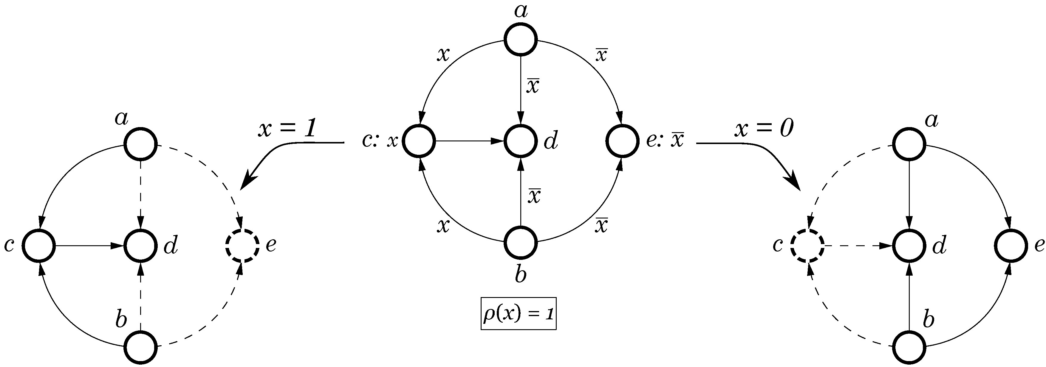
CPOG projections. An example of a graph and its two projections is presented in
Figure 4. The leftmost projection is obtained by keeping in the graph only those vertices and arcs whose conditions evaluate to 1 after substitution of variable
x with 1 (such projections are conventionally denoted by
). Hence, vertex
e disappears (shown as a dashed circle
), because its condition evaluates to 0:
. Arcs
disappear for the same reason; they are shown as dashed arrows
. The rightmost projection is obtained in the same way with the only difference that variable
x is set to 0; it is denoted by
, respectively. Note that although the condition of arc
evaluates to 1 (in fact it is constant 1) the arc is still excluded from the resultant graph because one of the vertices it connects, viz. vertex
c, is excluded and naturally an arc cannot appear in a graph without one of its vertices. Each of the obtained projections can be regarded as specification of a particular behavioural scenario of the modelled system, e.g., as specification of a processor instruction. Potentially, a CPOG
can specify an exponential number of different instructions (each composed from atomic actions in
V) according to one of
different possible opcodes. We can now establish a formal correspondence between CPOGs and instruction sets.
Figure 4.
CPOG projections: (left) and (right).
Figure 4.
CPOG projections: (left) and (right).
An
instruction is a pair
, where
ψ is the
instruction opcode (a vector of Boolean values), and
P is a partial order that specifies the
instruction behaviour or
microprogram [
11].
An instruction set, denoted by , is a set of instructions with unique opcodes, that is, for any , such that , all opcodes must be different.
Given a CPOG
there is a natural correspondence between its projections and instructions: an opcode
induces a partial order
, and paired together they form an instruction
according to the above definition. This leads to the following formal link between CPOGs and instruction sets. A CPOG
is a
specification of an instruction set
defined as a union of instructions
which are allowed by the restriction function
ρ:
Note that this definition automatically guarantees that no two instructions have the same opcode.
4. Design of Reconfigurable Microarchitectures
In this section we demonstrate how to use the CPOG model to build large instruction sets from basic building elements, how to introduce reconfigurability, and finally how to automatically derive an implementation for the specified microarchitecture.
4.1. Building Instruction Sets
CPOGs can be deconstructed by means of projections (
Section 3). The opposite operation, that is constructing a CPOG out of parts, is called
composition. This operation is essential for building large instruction sets from smaller ones, thus enabling modularisation, reuse, and incremental development.
Let instruction sets
and
be specified with graphs
and
, respectively, as in Equation (
1). Then their
composition has the CPOG specification
, where the vertex/arc conditions
are defined as
We call
H the
CPOG composition of
and
and denote this operation as
. Composition is defined only if
, as otherwise
and
contain instructions with the same opcode making the result ambiguous. It is possible to formally prove that ∪ is a commutative and associative operation and that
using the algebraic methods presented in [
8], which leads to the following important result:
.
Once an instruction set is built, it usually undergoes a set of transformations and optimisations which include modification of the set of computational units, changing opcodes of instructions or groups of instructions, modifying the instruction pipeline,
etc. Most of these transformations are outside the scope of this work and are defined in [
9]. In the following subsections we introduce two new transformaitons.
4.2. Mode-Specific Components
There are many ways in which we can implement a particular datapath component (e.g., a multiplier) and they all differ in their performance and energy-efficiency characteristics. If the energy budget of the system varies in runtime it may be beneficial to include more than one implementation in the processor: in this way, it would be possible to choose the most appropriate one in runtime according to the availability of energy and current application requirements. The CPOG model provides a convenient way of introducing such mode-specific component implementations into the processor microarchitecture.
Let
be the specification of an instruction set and
correspond to a datapath component whose implementation we would like to make mode-specific. This can be achieved by the CPOG transformation called
vertex splitting. The operation transforms
H in the following way:
Vertex v is replaced by two vertices and , corresponding to two mode-specific implementations of the component. In other words, vertex v is split into two new ones ;
Arcs are replaced with two arcs and and, similarly, arcs are replaced with two arcs and . Arc conditions are preserved;
Set of variables
X is extended with a new
mode variable m that is used to determine which of the two implementations is active. Mode variables are changeable in runtime from software, thus facilitating the cross-layer feedback control illustrated in
Figure 1;
Function ρ is unchanged, thus instruction opcodes are not affected by this transformation and the new microarchitecture has no penalties in terms of compactness of the instruction encoding;
The new vertices get conditions and , where is the condition that was assigned to the removed vertex v.
The vertex splitting transformation is illustrated in
Figure 5. This transformation increases area and leakage current, but the latter can be mitigated by power gating using the mode variable
m to disconnect inactive components from the power supply. As a side benefit, vertex splitting improves the system’s fault tolerance: if one of the two components fails, we can disable it and use the other component regardless of the current performance
vs. energy-efficiency strategy. In this way the system will be able to maintain the correct functionality but the degree of power-proportionality will be decreased.
Figure 5.
Vertex splitting.
Figure 5.
Vertex splitting.
Note that this transformation can also be defined in terms of CPOG composition of two mode-specific instruction sets: where (resp., ) corresponds to CPOG H with vertex v replaced with vertex (respectively, ). The resulting CPOG specifies the same instruction set but can be derived in a simpler and more compositional manner.
4.3. Concurrency Management
It is often the case that an instruction can be executed with different degrees of concurrency. For example, we can typically perform an ALU operation either concurrently with fetching the next instruction opcode or in sequence with it.
Consider two actions a and b. If they have no mutual dependencies in terms of functionality then they can seemingly be executed concurrently. However, they both consume a certain amount of power and this fact should not be ignored when designing power-aware systems. If concurrent execution of a and b exceeds the available power budget, the supply voltage may drop significantly which can potentially lead to the failure of the whole system. On the other hand, executing a and b only in sequence may be too conservative and will result in a slower system. How can we deal with this situation?
We propose to provide support for both execution scenarios in the microarchitecture and choose the most appropriate one according to the current power budget in runtime. Using the CPOG specification model this can be achieved by making the arc between vertices a and b conditional: . Now if the mode variable m is equal to 0 then components a and b will be executed concurrently (the arc disappears when ); otherwise, when execution of a and b will be scheduled in sequence, hence limiting the peak power consumption.
4.4. Synthesis of Microcontroller
As soon as all the intended manipulations with the instruction set are performed, we can proceed to the stage of mapping the resultant CPOG into Boolean equations to produce a physical implementation of the specified microcontroller. In order to descend from the abstract level of atomic actions to the physical level of digital circuits the following signal-level refinements are necessary.
To interface with an asynchronous datapath component
a it is possible to use the standard request-acknowledgement handshake
, as shown in
Figure 6. In case of a synchronous component
b the request signal is used to start the computation but, as there is no completion detection, the acknowledgement signal has to be generated using a matched delay [
12]. Also, there are cases when a matched delay has to be replaced with a counter connected to the
clock signal to provide an accurate multi-cycle delay—see the interface of component
c in the same figure. Note that we do not explicitly show synchronisers [
13] in the diagram; it is assumed that components
b and
c are equipped with the necessary synchronisation mechanisms to accept asynchronous requests from the microcontroller.
Figure 6.
Datapath interface architecture.
Figure 6.
Datapath interface architecture.
To explicitly specify handshake signals it is possible to perform a graph transformation explained in
Figure 7. Every atomic action
is split into a pair of events
and
standing for rising transitions of the corresponding handshake signals. If there are two occurrences of an atomic action, e.g.,
and
, then both vertices are split (we use superscripts to distinguish different occurrences of the same event), etc. Semantically, when an atomic action
is ready for execution, the controller should issue the request signal
to component
a; then the high value of the acknowledgement signal
will indicate completion of
a.
Notice that the microcontroller does not reset handshakes until all of them are complete. This leads to a potential problem: a component cannot be released until the instruction execution is finished. To deal with this we decouple the microcontroller from the component, see box “decouple" in
Figure 6 and its gate-level implementation in
Figure 8a. Also, when a component
b is used twice in an instruction we combine two handshakes
into one using the merge controller, see
Figure 8b. Merge controllers can only be used if the requests are mutually exclusive. If this is not the case, as e.g., for concurrent actions
and
, then we have to set an arbiter guarding access to the component. Its implementation consists of the merge controller and the mutual exclusion (ME) element [
13], see
Figure 8c.
Figure 7.
Signal-level refinement.
Figure 7.
Signal-level refinement.
Figure 8.
Handshake controllers: (a) Decouple; (b) Merge and (c) Arbiter.
Figure 8.
Handshake controllers: (a) Decouple; (b) Merge and (c) Arbiter.
Finally, the refined graph can be mapped into Boolean equations. An event associated with vertex
is enabled to fire (
is excited) when all the preceding events
have already fired (
have been received) [
8]:
where
stands for Boolean implication indicating “b if a” relation. Mapping is a simple structural operation, however the obtained equations may be suboptimal and should undergo the conventional logic minimisation [
8,
11] and technology mapping [
7] procedures.
It is interesting to note that the size of the microcontroller does not depend on the number of instructions directly. There are conditions in all the resultant equations; the average size of these conditions is difficult to estimate, but in practice we found that the overall size of the microcontroller never grows beyond .
5. Reconfigurable 8051 Microcontroller
In this section we describe our power-proportional implementation of the Intel 8051 microprocessor with reconfigurable microarchitecture designed using the CPOG model.
The instruction set of Intel 8051 contains 255 instructions and our implementation supports all of them. We generally follow the standard 8051 architecture with two on-chip RAMs; the program is stored in a reprogrammable off-chip ROM. However several important changes were made:
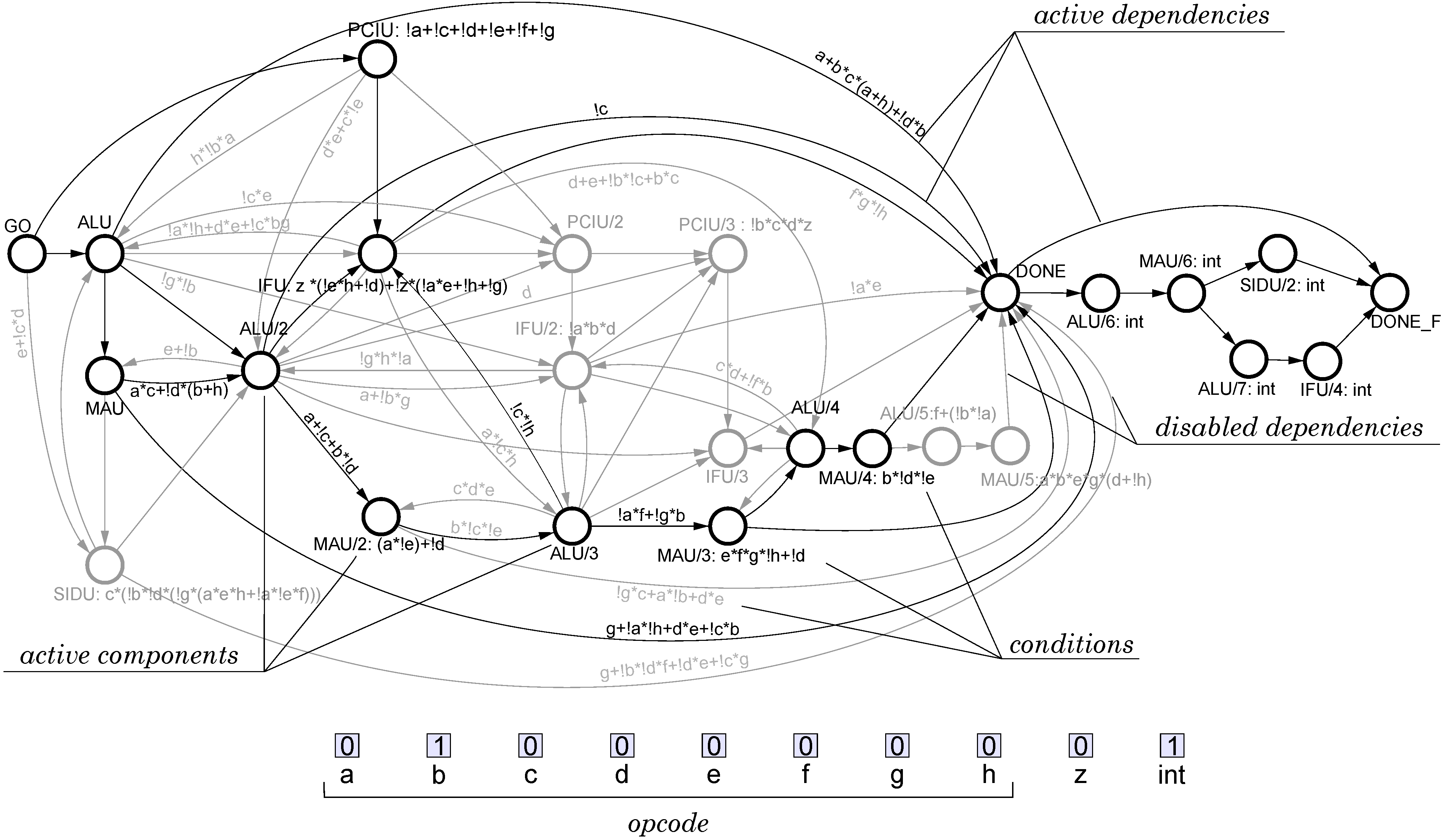
Figure 9 shows the top-level view of the microprocessor architecture. The shaded block corresponds to the central control unit (the main design objective), the rest of the blocks correspond to datapath units. The top-level CPOG specification of the microprocessor is shown in
Figure 10. Note that the main datapath block, the Arithmetic Logic Unit (ALU), is a complicated subsystem with its own control unit and multi-mode operation; its microarchitecture was designed similarly to the top-level one.
Figure 9.
Architecture of the designed microprocessor (dashed lines represent a 1 bit wide control signal line, the bit-width of other connections is shown in brackets).
Figure 9.
Architecture of the designed microprocessor (dashed lines represent a 1 bit wide control signal line, the bit-width of other connections is shown in brackets).
Figure 10.
CPOG model of Intel 8051 control logic.
Figure 10.
CPOG model of Intel 8051 control logic.
5.1. Design Flow
The first stage in microprocessor design is the specification of instructions. Each instruction corresponds to a schedule of primitive computation steps such as data transfer, arithmetic operation, memory access, etc., performed by datapath components. Overall, the proposed microprocessor design flow consists of the following steps:
Extraction of datapath components. We refine the architecture to the level of computational units and behavioural scenarios. There are several ways in which this can be done: (i) direct refinement from software; (ii) specification with Architecture Description Languages [
14,
15] and (iii) formalisation of existing instruction specifications (e.g., ISA manual). In our case we had a complete description of the microprocessor, its instruction set, and architecture details [
16], therefore the last option was the most suitable.
Table 1 describes five computational units extracted from the 8051 instruction set.
Partial order specification of instructions. The behaviour of each instruction is captured by a partial order (PO) in which the required computation units need to be activated. Different instructions often have the same PO representations; we grouped all 8051 instructions into 37 classes according to their POs, with the largest class containing 60 instructions.
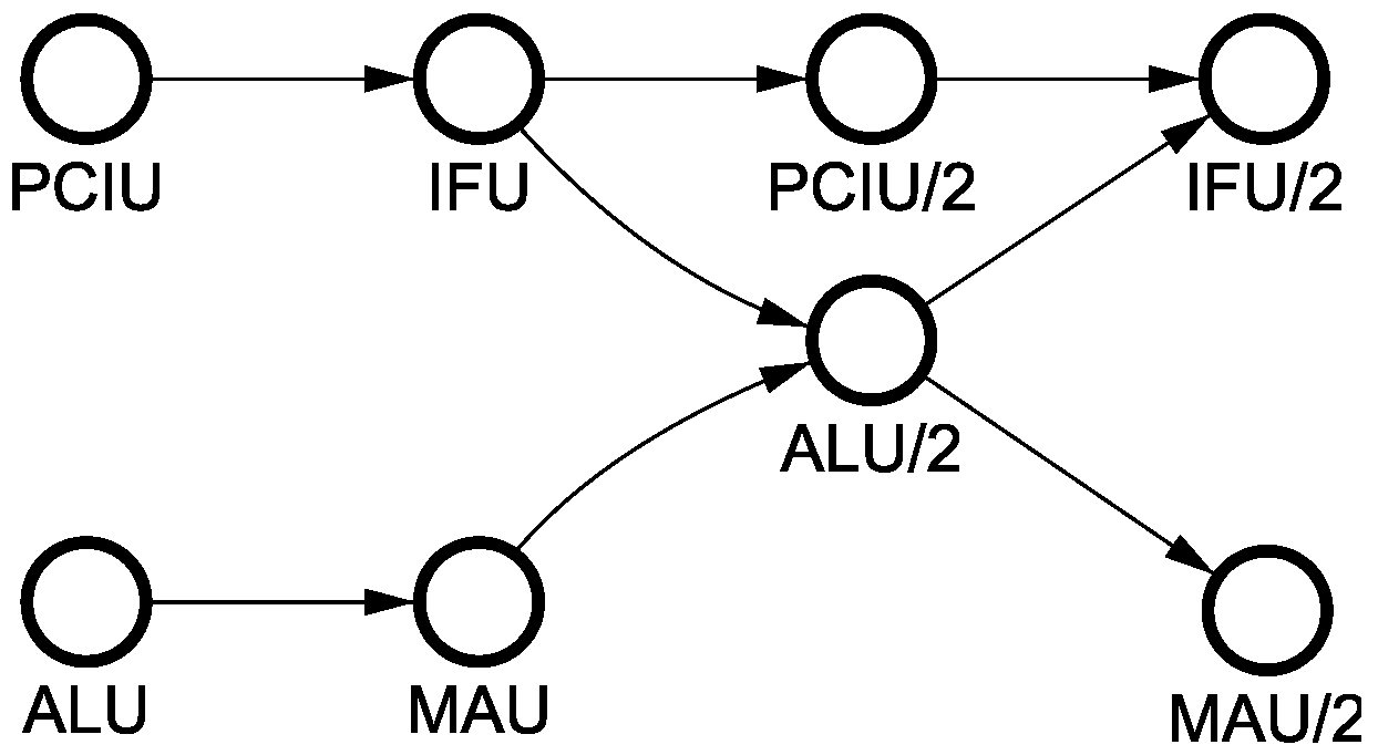
Figure 11 shows the PO representation of one of the classes, which corresponds to a group of 17 instructions such as, for example,
ADD A, immediate that performs addition of the accumulator and an immediate constant. We first read data from the accumulator (ALU followed by MAU) while concurrently fetching an immediate constant (PCIU followed by IFU). Then we perform addition (ALU/2) concurrently with another increment of PC, and finally write the result back into accumulator (MAU) and fetch the next instruction (IFU/2). Many other instructions have the same behaviour:
ADDC A, immediate;
SUBB A, immediate;
ORL A, immediate;
ANL A, immediate, etc.
Table 1.
List of datapath units.
Table 1.
List of datapath units.
| Name | Description |
|---|
| PCIU | Program Counter Increment Unit is responsible for incrementing the Program Counter—a special register pointing to the address of the next instruction in the program memory. |
| IFU | Instruction Fetch Unit loads the operational code of the current instruction from the program memory using the address stored in Program Counter. |
| MAU | Given an address pointer and data, the Memory Access Unit can access the internal and external RAM. |
| ALU | Arithmetic Logic Unit is the main computation unit responsible for performing arithmetic and logic operations in the microprocessor. To make it adjustable towards a wide range of operating conditions and application requirements, we designed two sets of ALU datapath components, each optimised to work in a specific mode: one optimised for performance and the other one for energy efficiency. |
| SIDU | Stack pointer Increment/Decrement Unit, as the name suggests, is in charge of incrementing and decrementing the stack pointer. |
Figure 11.
Partial order (PO) for ADD instruction.
Figure 11.
Partial order (PO) for ADD instruction.
Encoding of partial orders. In order to distinguish between the POs, we need to encode them. The codes can either be assigned arbitrarily or can be provided as part of system specification. Importantly, the size and latency of the final microcontroller circuit depends significantly on the chosen encoding of the scenarios. There are several types of encoding that can be used, such as one hot, matrix, balanced, and Huffman encoding [
17]. A new technique for optimal encoding was recently introduced in [
18], but it was unable to process our set of POs due to high complexity of the optimal encoding algorithm, hence we used Huffman encoding in our design.
CPOG synthesis. Once all instructions are represented as POs and encoded, we can synthesise a CPOG containing all of them as described in
Section 4. We used the Workcraft framework [
19] which automates the specification and synthesis stages. The resulting CPOG is shown in
Figure 10.
Mapping. The final stage is mapping of the CPOG representation into a set of logic gates to produce a physical implementation (a gate-level netlist) of the specified microcontroller. Finally, we can translate the obtained Boolean equations into VHDL, Verilog or other HDL language to use in standard EDA flow.
5.2. Adaptability Features
To enable power-proportionality in a wide range of power supply and service demand conditions, we designed two sets of computation units: one optimised for performance and the other one optimised for energy efficiency. Depending on whether there is a shortage of energy or on any other restrictions imposed by an active application, we can choose the most appropriate datapath unit to be used during an instruction execution. The decision can be made at different levels of system control: software level, sensors, external signals, etc.
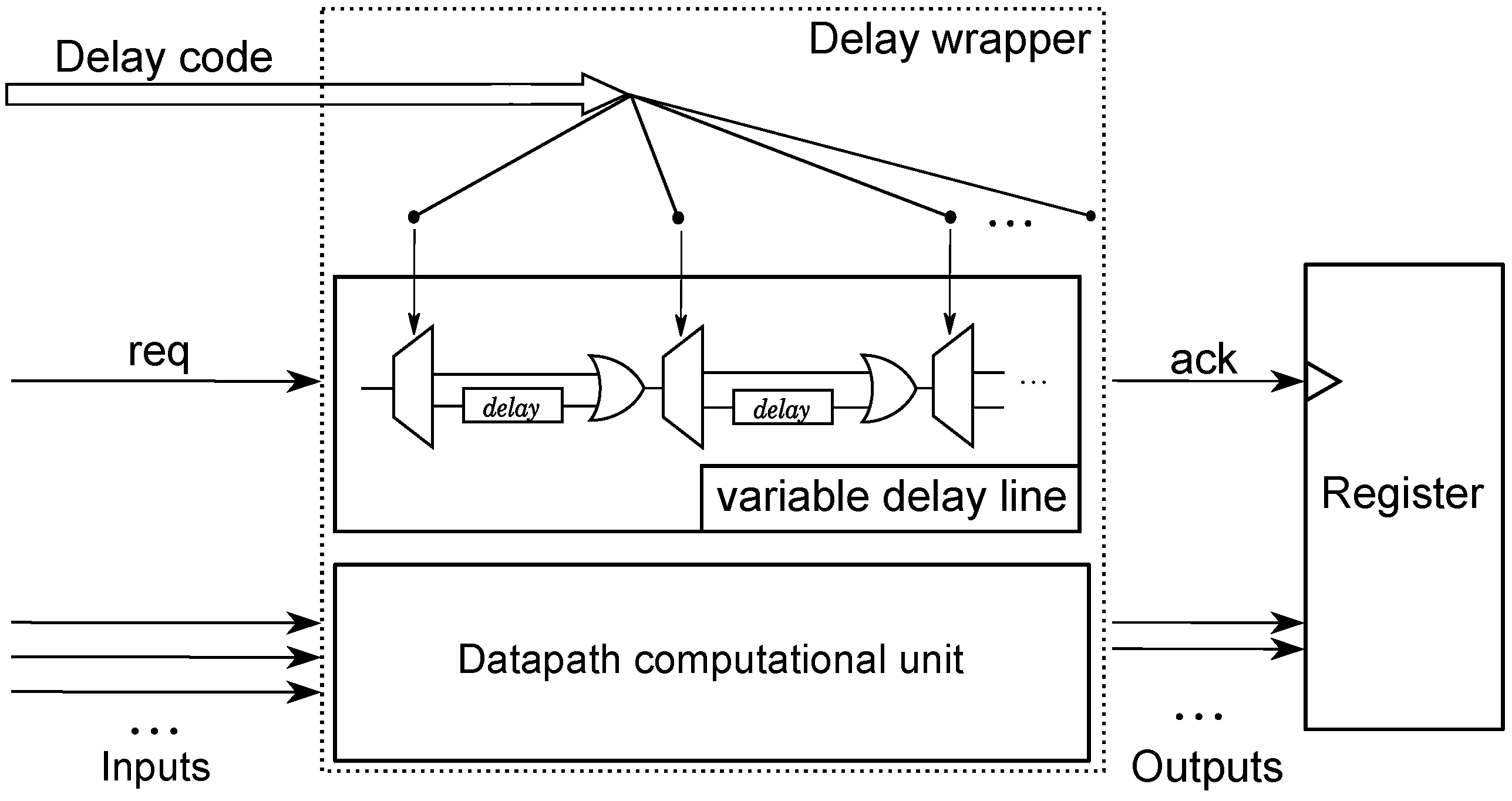
Our implementation of self-timed datapath components is based on bundled-data approach, where each component is accompanied with a matching delay line to signal completion of its computation. In order to correctly function in a wide range of operating conditions (e.g., supply voltage or temperature), a component needs to adjust the latency of its completion signal. We addressed this issue by use of
adjustable delay lines, whose latency is selectable by the
delay code at runtime, as shown in
Figure 12.
Figure 12.
Adjustable delay lines.
Figure 12.
Adjustable delay lines.
5.3. Experiments
We implemented the microprocessor in STMicroelectronics 130nm CMOS technology process and conducted experiments to evaluate the level of adaptability we can achieve using the presented approach. In this section we report results of our measurements. The nominal supply voltage of the chip is 1.2 V; we varied the supply voltage in the range from 0.22 V to 1.5 V and observed the following:
0.89 V to 1.5 V: the chip works in full capability mode;
0.74 V to 0.89 V: at 0.89 V the RAM starts to fail; the chip operates using internal registers only;
0.22 V to 0.74 V: at 0.74 V the Program Counter unit starts to fail, so the chip gets stuck at executing the same instruction forever. The control logic synthesised using the CPOG model continues to operate correctly down to 0.22 V.
It should be noted that within the above-indicated range of 0.22–0.74 V, somewhere below 0.5 V, most of the microprocessor’s hardware is subjected to work in the near-threshold and even sub-threshold regime. Our implementation was based on standard STM cells, therefore we were not surprised by the fact that some registers like the Program Counter began to fail in this range. However, the important knowledge that we gleaned from testing our processor was that that the control circuitry, even though built of standard cells, was still operational in the sub-threshold regime. This shed light on how we can build future reconfigurable and power-proportional systems that would be able to operate in parts under different supply voltage levels.
We can conclude that our chip can work in dual-memory mode in the voltage range from 0.89 V to 1.5 V. This mode is to be used for applications requiring high-performance and large memory. The single-memory mode available in the voltage range from 0.74 V to 0.89 V can be used for low-power and scratchpad memory applications.
In terms of performance, we measured the range from 67 millions of instructions per second at the nominal voltage of 1.2 V down to 2700 instructions per second at 0.25 V. Note that since the Program Counter fails below 0.74 V the processor starts executing the same instruction forever.
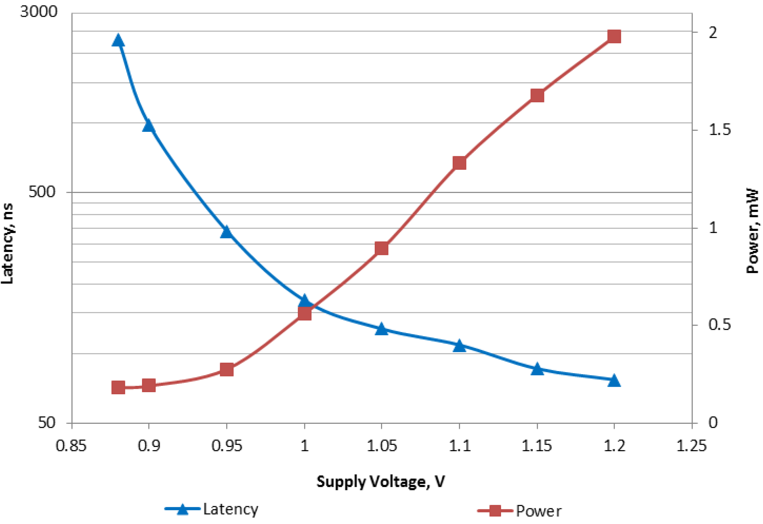
Figure 13 shows measurements of latency and power consumption of the ADD instruction run in the voltage range from 0.88 V to 1.2 V. In our expertiments other instructions exhibited similar latency/power characteristics.
Figure 13.
Measurements for ADD instruction.
Figure 13.
Measurements for ADD instruction.
To compare our implementation with existing Intel 8051 designs we run the Dhrystone V2.1 testbenches [
20], see the summary of obtained results in
Table 2. Sync 80C51, H8051 and DS89C420 are synchronous designs; the first two employ non-pipeline architectures and the last one has a pipelined architecture. Async 80C51 is an asynchronous counterpart of the Sync 80C51 design. Lutonium is another asynchronous implementation which utilises a highly parallel processing with a deep pipeline architecture; it has high MIPS rate and power consumption. Nanyang A8051 is a self-timed, ultra low power (and hence low performance) implementation. After normalising the results with respect to the technology difference, our implementation is clearly placed between ultra low power design (runs twice as fast) and the highly parallel version (consumes 20 times less power).
Table 2.
Performance comparison with other 8051 versions.
Table 2.
Performance comparison with other 8051 versions.
| Processor | Technology | 11 cm MIPS | Average power, mW | MIPS per W | Energy, pJ per instruction |
|---|
| Sync 80C51 [21] | 3.3 V, 350 nm | 4 | 40 | 100 | 10000 |
| Async0C51 [21] | 3.3 V, 350 nm | 4 | 9 | 44 | 2250 |
| H8051 [22] | 3.3 V, 350 nm | 4 | 44.7 | 89.5 | 11175 |
| Lutonium [23] | 1.8 V, 180 nm | 200 | 100 | 1800 | 500 |
| DS89C420 [24] | 1.1 V, 350 nm | 11 | 18.52 | 600 | 1684 |
| Nanyang A8051 [25] | 1.1 V, 350 nm | 0.6 | 0.07 | 8000 | 130 |
| Lutonium [23] | 1.1 V, 180 nm | 100 | 20.7 | 4830 | 207 |
| Proposed 8051 | 1.2 V, 130 nm | 1.5 | 0.74 | 2027 | 493 |
