Abstract
A threshold voltage (Vth) controllable multigate FinFET on a 10-nm-thick ultrathin BOX (UTB) SOI substrate have been investigated. It is revealed that the Vth of the FinFET on the UTB SOI substrate is effectively modulated thanks to the improved coupling between the Si channel and the back gate. We have also carried out analysis of the Vth controllability in terms of the size dependence such as the gate length (LG) and the fin width (TFin).
1. Introduction
Recently, complementary metal oxide semiconductor (CMOS) device technology has faced several difficulties. Short channel effects (SCEs) such as threshold voltage roll-off and sub-threshold slope (s-slope) degradation caused by the reduced drivability of the gate electrode cause significant increase in power consumption and become a limiting factor in MOS devices [1,2]. In addition, variability of the CMOS device increases and reduces the yield of the CMOS circuit [3]. Fortunately, fin-type MOS field effect transistors (FinFETs) provide a potential solution for the nano-scale CMOS technology thanks to their high drive current while maintaining a low sub-threshold (s-) slope [4,5]. However, for FinFETs, adjustment of the threshold voltage (Vth) is still a tough issue. One way of controlling the Vth of the MG MOSFET is to tune the work function of the gate electrode [6]. However, selection of the metal with the appropriate work function is difficult. A doped silicon channel is effective for Vth tuning; however, it cause severe variability due to the random dopant fluctuation [7,8].
The other way of controlling the Vth of the FinFET is by using the substrate back bias using the SOI substrate [9,10]. In fact, Vth control by the substrate back bias has been investigated for the planar devices [11,12,13,14]. However, effectiveness of the back gate bias on the Vth of the FinFET is different due to the narrow channel. Recently, we have demonstrated a flexible Vth tuning for the FinFET by controlling the back bias using a 10-nm-thick ultra-thin (UT) buried oxide (BOX) silicon on insulator (SOI) substrate to demonstrate effectiveness of UTBOX for the vth control of the FinFET [15,16]. Moreover, we have flexibly controlled the Vth by adding the second gate of the independent-double-gate FinFET [17]. In this study, we have extended the analysis of Vth flexibility in terms of the LG and the TFin dependence of the Vth controllability using the 10 nm-thick UTBOX SOI substrate.
2. Experimental
2.1. MOS Capacitor
Prior to the device fabrication, we have evaluated the quality of the UTBOX by comparing the characteristics with thermal SiO2. The test structure used in this study is illustrated in Figure 1. The thermal SiO2 grown at 850 °C is covered with the chemical-vapor-deposited 50-nm-thick poly-Si. Ion implantation was carried out into the top Si layer to fabricate the gate electrode. The thermally grown SiO2 with the polycrystalline-Si electrode is used as a reference sample.
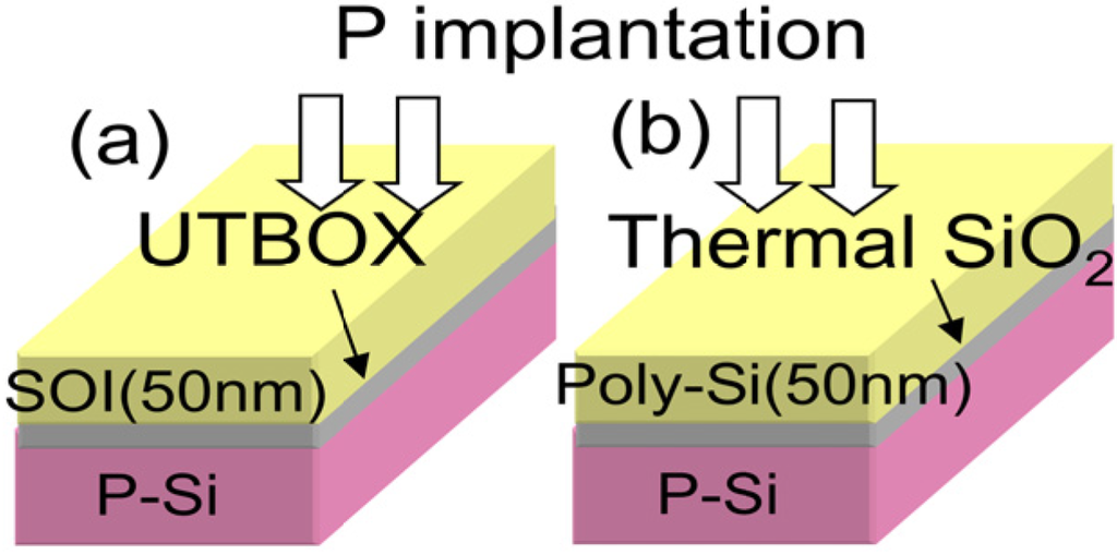
Figure 1.
The MOS capacitor test structure. (a) Ultrathin (UT) buried oxide (BOX) silicon on insulator (SOI) substrate; (b) Thermal SiO2 test structure.
2.2. Device Fabrication
In this study, we have used 200-mm UTBOX SOI wafers as an initial material and have fabricated the FinFET devices on a UTBOX SOI substrate. The ellipsometrically measured thickness of the UTBOX was 10 nm. We have also fabricated the FinFET on the 120-nm-thick BOX for comparison. The fabrication process flow is summarized in Figure 2. A 50-nm-thick non-doped silicate glass (NSG) layer and the electron beam (EB) resist masks were formed to make hard masks on the wafer. To fabricate vertical Si-fins, the SOI layer was etched by a conventional reactive ion etching (RIE) using a Cl2 inductively coupled plasma (ICP) as schematically shown in Figure 2. After the Si-fin etching, a 2.5-nm-thick gate-oxide was formed at 850 °C followed by the TiN and n+ polycrystalline-Si (poly-Si) gate formation using EB lithography and the RIE. After the gate electrode was formed, a shallow implantation into the extension of the source/drain (S/D) was performed. To distribute impurity atoms uniformly into the vertical channel, 60-degree tilted implantation was carried out at an acceleration energy of 5 keV and a dose of 2 × 1014 cm−2 in each side [18]. S/D implantation was performed at an acceleration energy of 10 keV and a dose of 1.5 × 1015 cm−2 after a 50-nm-thick gate-sidewall was formed by using CVD grown SiO2. The acceleration energy was set to 10 keV to preserve the seed-crystal layer for the recrystalline annealing. Figure 3 shows the cross sectional transmission electron microscope (TEM) image of the fabricated FinFET and the plane scanning electron microscope (SEM) image of the SRAM cell. The FinFET on the UTBOX SOI is successfully fabricated. The fin height was measured as 30 nm.
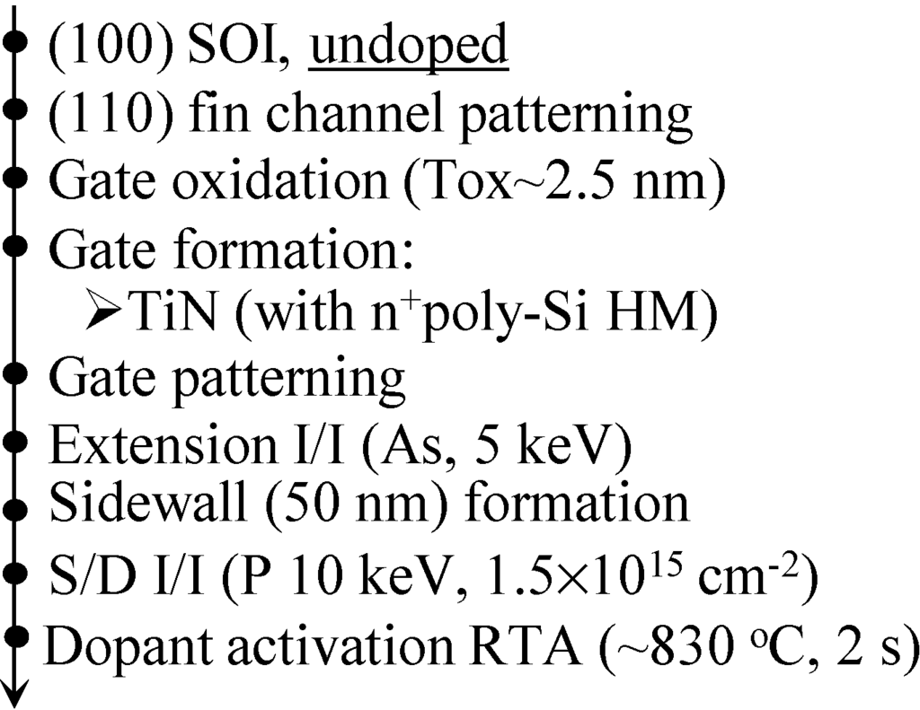
Figure 2.
Schematic process flow for the fabrication of fin-type MOS field effect transistors (FinFETs).
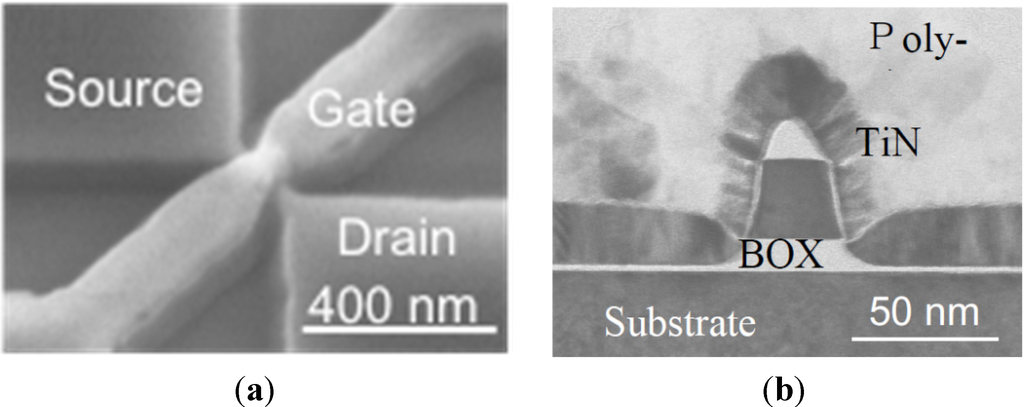
Figure 3.
(a) SEM image of the fabricated FinFET, (b) Cross-sectional TEM image of the fabricated FinFET.
3. Results and Discussion
Figure 4 compares capacitance-voltage (C-V) characteristics of the UTBOX layer and the thermal SiO2. It is found that the C-V characteristics of the UTBOX layer are similar to that of the thermal SiO2. The capacitance equivalent thickness (CET) of the UTBOX is measured as 11.5 nm and the uniformity of the UTBOX thickness is as good as that of the thermal SiO2. Figure 5 compares the current-voltage (I-V) characteristics of the MOS capacitor using the UTBOX and the thermal SiO2. The I-V characteristics of the MOS capacitor with the same dielectric thickness are also the same. Figure 6 shows the gate voltage of the MOS capacitor where the leakage current exceeds 10−7 A/cm2 as a function of the oxide thickness. The gate voltage of the UTBOX completely follows the trend of the thermal SiO2. These results strongly indicate that quality of the UTBOX and its interface is as good as that of the thermal SiO2.
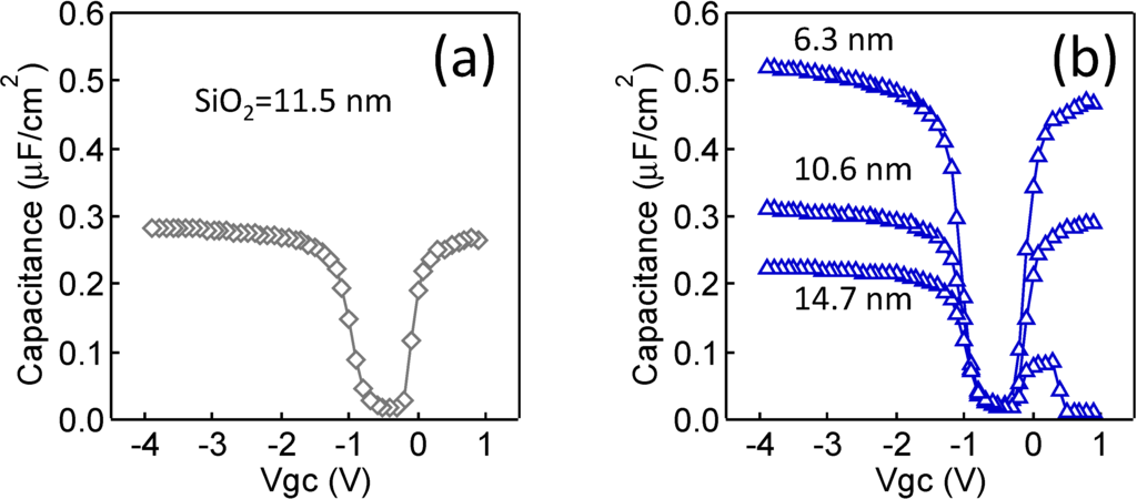
Figure 4.
C-V characteristics of the MOS capacitor: (a) UTBOX; (b) thermal SiO2.
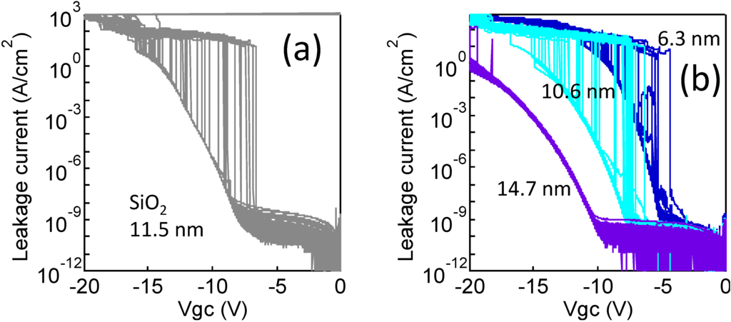
Figure 5.
I-V characteristics of the MOS capacitor: (a) UTBOX; (b) Thermal SiO2. The glitches in the figure indicate the fluctuation of the breakdown in different MOS capacitors.
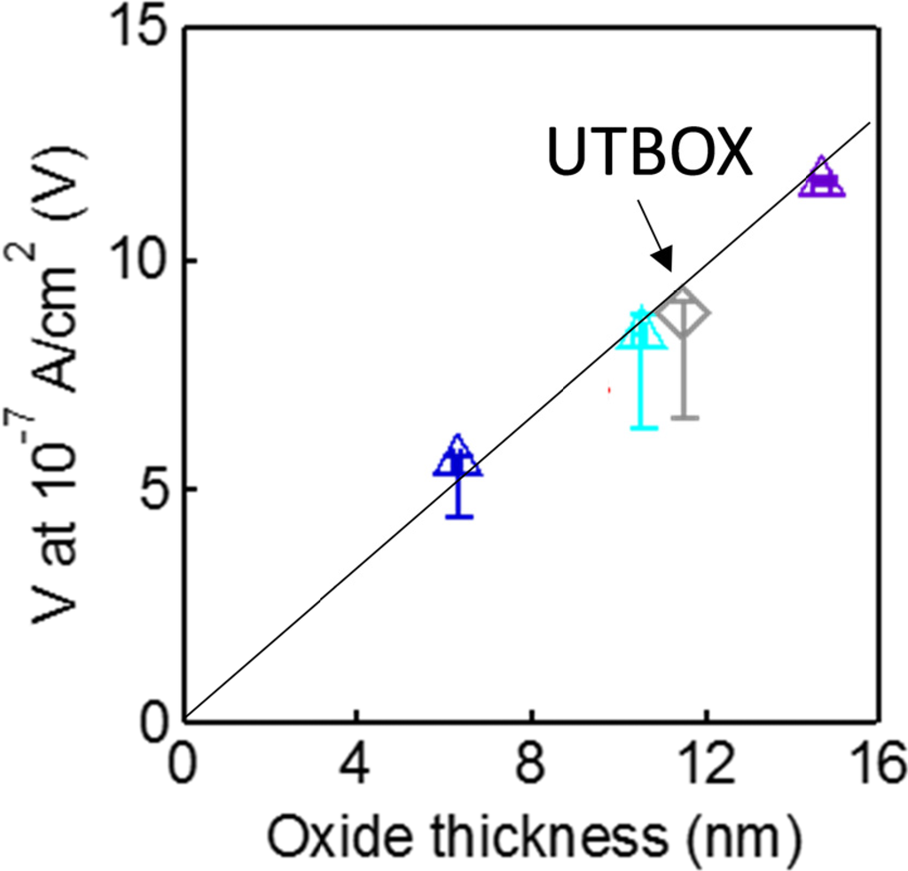
Figure 6.
The gate voltage of the MOS capacitor where the leakage current exceeds 10−7 A/cm2 as a function of the oxide thickness.
Figure 7 shows the ID-VG characteristics of the FinFET with the UTBOX SOI and the conventional thick BOX SOI. We revealed that the ID-VG characteristics the FinFET on the UTBOX SOI could be flexibly modified by applying the substrate bias voltage. We also found that the FinFET with the thick TFin was effective for the Vth modulation. Figure 8 shows the Vth as a function of the Vsub. The Vth is taken by the constant current method. The ID-VG characteristics are fixed and thus the Vth is fixed with the conventional thick BOX substrate. Also, the effectiveness of the thick TFin for the Vth modulation is clearly shown. This is caused by the increased coupling between the Si body and the back gate.

Figure 7.
ID-VG characteristics of the FinFETs with the UTBOX and the conventional thick BOX SOI. The substrate bias voltages are ranging from −1 V to 1 V with a 0.5 V step: (a) TFin= 50 nm, LG= 40nm, BOX 10 nm; (b) TFin= 70 nm, LG= 40nm, BOX 10 nm; (c) TFin= 50 nm, LG= 40nm, BOX 120 nm.
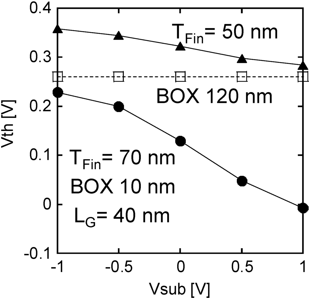
Figure 8.
The Vth of the FinFET as a function for the substrate bias.
Figure 9 summarizes the size dependence of the body factor γ determined by the ΔVth/ΔVsub. The γ is increased by increasing the TFin supporting the effectiveness of the thick TFin for the Vth modulation. In contrast to the TFin dependence, the opposite trend with the LG is shown and the γ is increased by reducing the LG. Moreover, the γ exceeded more than 0.1 with the 70-nm-thick fin thanks to the 10-nm-thick UTB SOI. To understand this LG dependence, the short channel effect represented by the Vth roll-off is evaluated as shown in Figure 10. We found that the Vth roll-off is more sever for the FinFET with the positive Vsub, small LG, and the thick TFin. Thus, the γ becomes higher for the FinFET with the small LG and the thick TFin due to the Vth roll-off. This result is consistent with the previous report on the nanowire FET with the 20-nm-thick BOX SOI [19].
Figure 11 shows the s-slope of the FinFET as a function of the LG. The increase of the s-slope by reducing the LG due to the short channel effect is clearly shown. It is noteworthy that the s-slope of the FinFET with the negative Vsub is smaller than that of the positive Vsub. Thus, the body bias is also effective for suppressing the short channel effects.
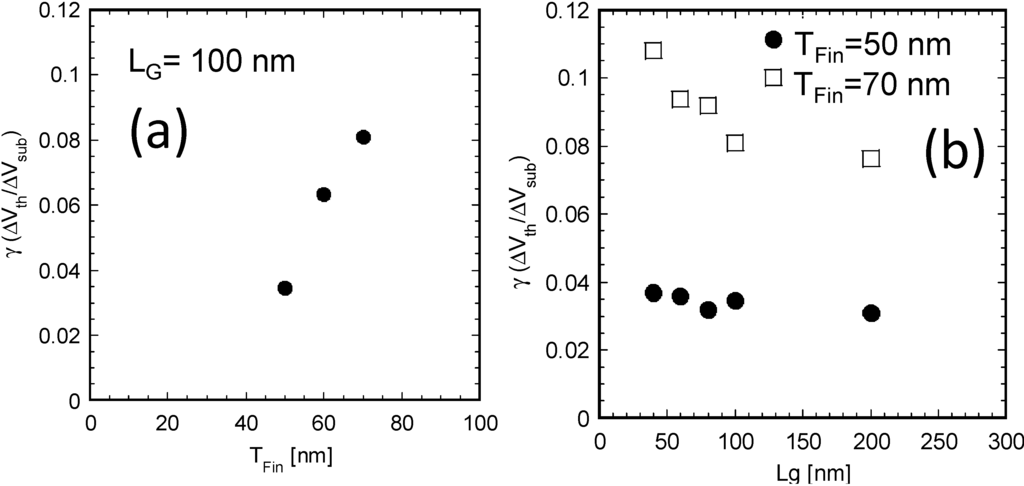
Figure 9.
The size dependence of the body factor γ determined by the ΔVth/ΔVsub, (a) TFin dependence; (b) LG dependence.
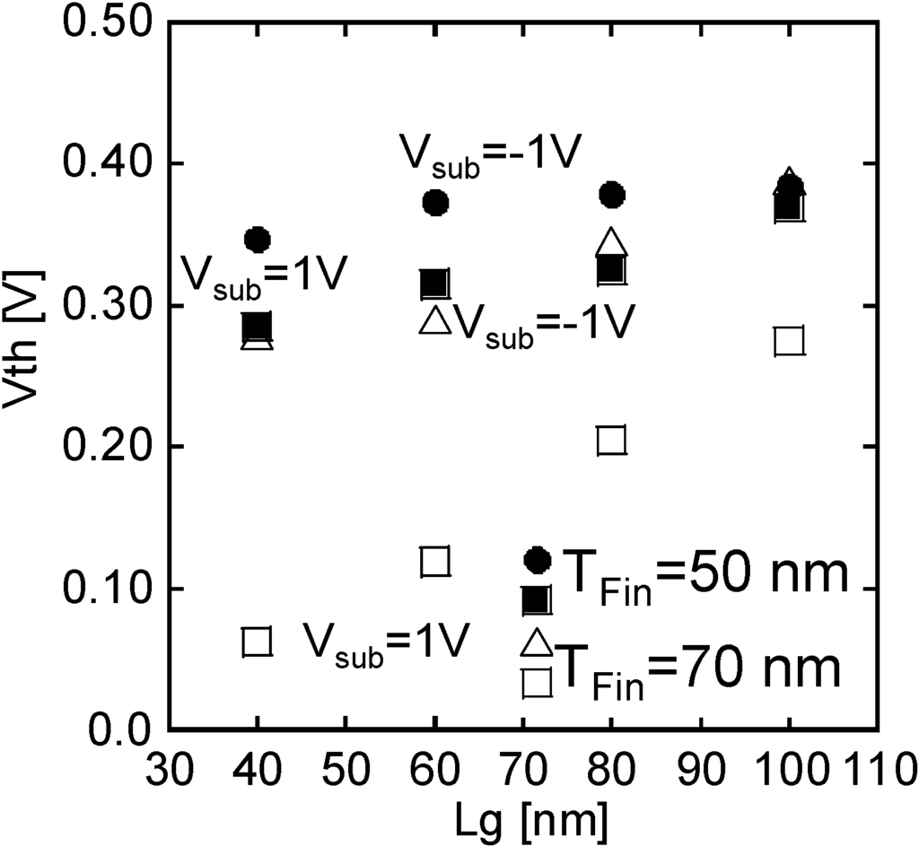
Figure 10.
Vth roll-off characteristics for the FinFET with the different TFin.
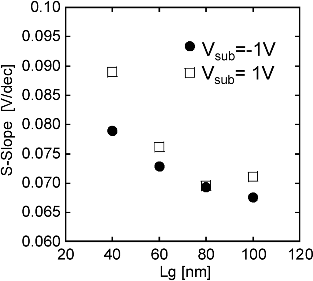
Figure 11.
The s-slope of the FinFET as a function of the LG.
4. Conclusions
The Vth controllable FinFETs using the 10-nm-thick UTB SOI substrate have been successfully fabricated and controllability of the Vth is analyzed in terms of the size dependence. It is shown that the body factor is increased by increasing the TFin and reducing the LG and it exceeded above 0.1 thanks to the 10-nm-thick UTBOX SOI. The back gate bias is also effective for the reduction of the s-slope. Thus, the UTBOX SOI is promising for the modulation of the Vth and improvement of the short channel effects for the scaled FinFET.
Author Contributions
Kazuhiko Endo fabricated the devices and coordinated the overall research. Shinji Migita fabricated the MOS capacitor and investigated quality of the BOX layer. Yuki Ishikawa, Takashi Matsukawa, Shin-ichi O’uchi, Junji Tsukada fabricated the devices. Hitomi Yamauchi observed TEM images. Wataru Mizubayashi, Yukinori Morita, Hiroyuki Ota, and Meishoku Masahara designed the fabrication process and discussed the results.
Conflicts of Interest
The authors declare no conflict of interest.
References
- Yan, R.-H.; Ourmazd, A.; Lee, K. Scaling the Si MOSFET: From Bulk to SOI to Bulk. IEEE Trans. Electron Devices 1992, 39, 1704–1710. [Google Scholar] [CrossRef]
- Yong, K. Short-Channel Effect in Fully Depleted SOI MOSFET’s. IEEE Trans. Electron Devices 1989, 36, 399–402. [Google Scholar] [CrossRef]
- Mizuno, T.; Okamura, J.; Toriumi, A. Experimental study of threshold voltage fluctuations using an 8K MOSFET array. In Proceedings of the 1993 Symposium on VLSI Technology, Kyoto, Japan, 17–19 May 1993; pp. 41–42.
- Sekigawa, T.; Hayashi, Y. Calculated threshold-voltage characteristics of an XMOS transistor having an additional bottom gate. Solid State Electron 1984, 27, 827–828. [Google Scholar] [CrossRef]
- Hisamoto, D.; Lee, W.-C.; Kedzierski, J.; Takeuchi, H.; Asano, K.; Kuo, C.; Anderson, E.; King, T.-J.; Bokor, J.; Hu, C. FinFET-a self-aligned double-gate MOSFET scalable to 20-nm. IEEE Trans. Electron Devices 2000, 47, 2320–2325. [Google Scholar] [CrossRef]
- Matsukawa, T.; Endo, K.; Liu, Y.X.; O’uchi, S.; Ishikawa, Y.; Yamauchi, H.; Tsukada, J.; Ishii, K.; Sakamoto, K.; Suzuki, E.; et al. Dual Metal Gate FinFET Integration by Ta/Mo Diffusion Technology for Vt Reduction and Multi-Vt CMOS Application. Solid-State Electron. 2009, 53, 701–705. [Google Scholar] [CrossRef]
- Xiong, S.; Bokor, J. Sensitivity of Double-Gate and FinFET Devices to Process Variations. IEEE Trans. Electron Devices 2003, 50, 2255–2261. [Google Scholar] [CrossRef]
- Chian, M.H.; Lin, J.-N.; Kim, K.; Chuang, C.-T. Random Dopant Fluctuation in Limited-Width FinFET Technologies. IEEE Trans. Electron Devices 2007, 54, 2055–2059. [Google Scholar] [CrossRef]
- Nagumo, T.; Hiramoto, T. Design Guideline of Multi-Gate MOSFET with Substrate-Bias Control. IEEE Trans. Electron Devices 2006, 53, 3025–3031. [Google Scholar] [CrossRef]
- Park, S.J.; Jeon, D.-Y.; Montès, L.; Barraud, S.; Kim, G.-T.; Ghibaudo, G. Impact of channel width on back biasing effect in tri-gate MOSFET. Microelectron. Eng. 2014, 114, 91–97. [Google Scholar] [CrossRef]
- Ohtou, T.; Hiramoto, T.; Saraya, T. Variable-Body-Factor SOI MOSFET with Ultrathin Buried Oxide for Adaptive Threshold Voltage and Leakage Control. IEEE Trans. Electron. Devices 2008, 55, 40–47. [Google Scholar] [CrossRef]
- Ohtou, T.; Nagumo, T.; Hiramoto, T. Variable Body Effect Factor Fully Depleted Silicon-On-Insulator Metal Oxide Semiconductor Field Effect Transistor for Ultra Low-Power Variable-Threshold-Voltage Complementary Metal Oxide Semiconductor Applications. Jpn. J. Appl. Phys. Part 1 2004, 43, 3311–3314. [Google Scholar] [CrossRef]
- Tsuchiya, R.; Horiuchi, M.; Kimura, S.; Yamaoka, M.; Kawahara, T.; Maegawa, S.; Ipposhi, T.; Ohji, Y.; Matsuoka, H. Silicon on thin BOX: A new paradigm of the CMOSFET for low-power high-performance application featuring wide-range back-bias control. In Proceedings of the IEEE International Electron Devices Meeting, San Francisco, CA, USA, 13–15 December 2004; pp. 631–634.
- Majumdar, A.; Ren, Z.; Koester, S.J.; Haensch, W. Undoped-Body Extremely Thin SOI MOSFETs with Back Gates. IEEE Trans. Electron. Devices 2009, 56, 2270–2276. [Google Scholar] [CrossRef]
- Endo, K.; Migita, S.; Ishikawa, Y.; Liu, Y.; Matsukawa, T.; O’uchi, S.; Tsukada, J.; Mizubayashi, W.; Morita, Y.; Ota, H.; et al. Flexible Vth FinFETs with 9-nm-Thick Extremely-Thin BOX. In Proceedings of the IEEE SOI Conference, Napa, CA, USA, 1–4 October 2012.
- Endo, K.; Ishikawa, Y.; Liu, Y.; Matsukawa, T.; O’uchi, S.; Tsukada, J.; Migita, S.; Mizubayashi, W.; Morita, Y.; Ota, H.; et al. Analysis of Vth Flexibility in Ultrathin-BOX SOI FinFETs. In Proceedings of the IEEE S3S Conference, Monterey, CA, USA, 7–10 October 2013.
- Liu, Y.; Masahara, M.; Ishii, K.; Sekigawa, T.; Takashima, H.; Yamauchi, H.; Suzuki, E. A highly Vth-controllable 4T FinFET with an 8.5-nm-thick Si-fin channel. IEEE Electron Device Lett. 2004, 25, 510–512. [Google Scholar] [CrossRef]
- Endo, K.; Masahara, M.; Liu, Y.X.; Ishii, T.M.K.; Sugimata, E.; Takashima, H.; Yamauchi, H.; Suzuki, E. Investigation of N-Channel Triple-Gate Metal-Oxide-Semiconductor Field-Effect Transistors on (100) Silicon On Insulator Substrate. Jpn. J. Appl. Phys. 2006, 45, 3097–3100. [Google Scholar] [CrossRef]
- Ota, K.; Saitoh, M.; Tanaka, C.; Numata, T. Systematic Study of Back-Gate Bias Effects in Ultrathin-BOX Tri-gate (UTBT) Transistor with 10nm-Diameter Nanowire Channel. In Proceedings of the Solid State Device and Materials, Kyoto, Japan, 25–27 September 2012.
© 2014 by the authors; licensee MDPI, Basel, Switzerland. This article is an open access article distributed under the terms and conditions of the Creative Commons Attribution license (http://creativecommons.org/licenses/by/3.0/).