Article

Two-Layer Error Control Codes Combining Rectangular and Hamming Product Codes for Cache Error
1
Department of Electrical and Computer Engineering, University of Rochester, Rochester, NY 14627, USA
2
Department of Electrical Engineering & Computer Science, Massachusetts Institute of Technology, Cambridge, MA 02139, USA
*
Author to whom correspondence should be addressed.
J. Low Power Electron. Appl. 2014, 4(1), 44-62; https://doi.org/10.3390/jlpea4010044
Submission received: 12 November 2013 / Revised: 20 January 2014 / Accepted: 10 February 2014 / Published: 27 February 2014

Abstract

:
We propose a novel two-layer error control code, combining error detection capability of rectangular codes and error correction capability of Hamming product codes in an efficient way, in order to increase cache error resilience for many core systems, while maintaining low power, area and latency overhead. Based on the fact of low latency and overhead of rectangular codes and high error control capability of Hamming product codes, two-layer error control codes employ simple rectangular codes for each cache line to detect cache errors, while loading the extra Hamming product code checks bits in the case of error detection; thus enabling reliable large-scale cache operations. Analysis and experiments are conducted to evaluate the cache fault-tolerant capability of various existing solutions and the proposed approach. The results show that the proposed approach can significantly increase Mean-Error-To-Failure (METF) and Mean-Time-To-failure (MTTF) up to 2.8×, reduce storage overhead by over 57%, and increase instruction per-cycle (IPC) up to 7%, compared to complex four-way 4EC5ED; and it increases METF and MTTF up to 133×, reduces storage overhead by over 11%, and achieves a similar IPC compared to simple eight-way single-error correcting double-error detecting (SECDED). The cost of the proposed approach is no more than 4% external memory access overhead.

1. Introduction

Reliability is a main concern in future multi-core and many-core designs. On the one hand, technology scaling makes it possible to integrate ever-increasing numbers of transistors on a single chip, enabling a many-core system design; on the other hand, scaling has brought about an increase in various error sources, such as process, voltage and temperature (PVT) variation, electromagnetic radiation and device aging. Meanwhile, as the speed gap between processor and external memory increases, large volume and high density caches are required, exacerbating the reliability issue furthermore. Consequentially, it is necessary to provide fault tolerance for cache to improve system reliability in future many-core systems.
We can classify cache errors as hard or soft errors [1,2]. Hard errors, which are permanent and unrecoverable, may be caused by chip manufacturing defects, threshold voltage variations, or runtime effect, such as device aging and electrostatic discharge, and soft errors, which occur transiently and can be recoverable, are introduced by external particle strikes or other random noises. Traditionally, most soft errors manifest as single cell upset. However, as we approach the nanometer era, the probability of multi-bit upset increases significantly because a single particle strike can cause more cache cell upset. For example, [3] shows that 55% of soft errors are multi-bit fails, and error clusters up to 20 failed bits were found in static random-access memory (SRAM).
An ever-increasing cache error rate, especially multi-bit upset (burst error), requires high fault-tolerant mechanisms for cache to improve system reliability. Meanwhile, it is critical that latency, area and power overhead introduced by these fault-tolerant mechanisms must be minimized to meet the strict constraints of power and latency budget for future many-core systems. Similar to [4], we employ two-layer error control codes (ECC) for cache. Based on the low latency and power overhead of rectangular codes, and the high error correction capability of Hamming product codes, we propose a novel two-layer ECCs, combining the error detection capability of rectangular codes and the error correction capability of Hamming product codes in an efficient way, to improve system reliability while maintaining low area, power, and latency overhead [4]. The proposed approach is based on the following observations and facts:
  • The cache error rate increases for large volume and high density cache in many-core systems, and can compromise overall system reliability if not well-protected. Meanwhile, future many-core systems place a strict budget on fault-tolerant mechanisms in terms of latency, power and area overhead. Therefore, high reliability but low cost fault-tolerant mechanisms are required;
  • The encoding and decoding of rectangular codes, which simply consists of several exclusive or (XOR) gates, can be very fast compared to other error control code, such as Hamming and BCH codes. In contrast, Hamming product codes can provide high error correction capability at the cost of extra check bits overhead;
  • Much of cache lines in systems are clean, which means there is another copy in next-level memory. Therefore, it is enough to detect error in clean cache lines, and only correct error in dirty cache lines [5].
The remainder of this paper is organized as follows: Section 2 reviews various fault-tolerant mechanisms for cache design. In Section 3, the proposed two-layer error control codes combining rectangular codes and Hamming product codes is described; Section 4 provides experimental results about cache reliability, storage overhead, system performance, memory access overhead of the proposed approach and other alternative solutions existing in current literature; Conclusion and future work are presented in Section 5.

2. Related Works

In this section, we review various cache fault-tolerant methods existing in current literature. Our focus is on architectural level solutions, to which the proposed approach belongs. We also briefly explain circuit and device level techniques handling with cache error to provide background information.

2.1. Soft Error Management Techniques

To address cache soft errors, various error control codes (ECC) have been investigated and employed. For example, IBM Power 6 applies parity codes to L1 cache and single-error correcting double-error detecting (SECDED) codes to L2 cache [6]. For low soft error rate (SER) and low volume cache, these approaches can provide enough reliability with low area, power and latency cost. However, as SER and cache size increases, these simple ECC codes fail to protect the whole system. Chishti et al. employ four-bit segmented orthogonal Latin square codes (OLSC) to correct faulty cells [7]. The low-complexity OLSC codes can provide a low-latency encoding/decoding process but at the cost of too much redundancy. Half or a quarter of the cache is sacrificed to store ECC check bits, which degrade system performance significantly. Wilkerson et al. propose strong BCH codes, such as five-error correcting six-error detecting (5EC6ED) codes to address reliability issues in the case of high cache error rate [8]. However, simple ECCs are ineffective in handling increasing burst errors in aggressively scaled technologies; unfortunately, complex ECCs introduce large power, area and latency overhead.
One general solution to burst errors is interleaving [9,10]. Generally, two types of interleaving, inter-cacheline interleaving and intra-cacheline interleaving, have been proposed. Inter-cache line interleaving distributes burst errors into different cache lines and applies ECC to each cache line. However, this leads to unnecessary cache line access because we need to read/write multiple cache lines even if only one is required. The power overhead introduced by unnecessary cache line access can be expensive, especially considering the increasing bit line length of the large volume cache adopted by many-core systems. The intra-cache line divides one single cache line into several sub-blocks and applies ECC to each sub-block. These inter-cacheline and intra-cacheline interleaving approaches can improve random error control mechanisms by making burst errors look like random errors. However, in some cases, it will also make random errors look like burst errors and introduce extra latency or power consumption overhead.
Kim et al. propose a two-dimensional ECC to deal with multi-bit clustered errors [11]. In the proposed scheme, the combination of a single error detection parity code and intra-cacheline interleaving is applied in the horizontal direction for each cache line; meanwhile, for all cells in one column, similar error control mechanisms are employed in the vertical direction. The proposed method can effectively address burst errors in both horizontal and vertical directions. However, it fails to address random errors and becomes ineffective as the soft error rate (SER) increases with technology scaling. Meanwhile, the proposed two-dimensional error control coding introduces a large area overhead (25%) and requires an extra cache read-modify-write operation of vertical check bits for every cache write access, worsening system energy efficiency.
Yoon et al. propose a so-called memory-mapping ECC, addressing soft errors while reducing storage overhead [5]. The proposed approach applies simple ECCs to all cache lines and stores complex ECCs into next-level memory. Specifically, the paper uses single-error detecting parity codes with eight-way intra-cacheline interleaving to detect burst errors and to store the interleaved SECDED codes in next-level memory to correct soft errors once they have been detected. In the normal case, only parity decoding will be performed to detect errors. In the case of error detection, extra SECDED check bits will be loaded to correct the error. The actual error correction capability of the proposed memory-mapping ECC is equal to eight-way intra-cacheline interleaving SECDED codes while achieving similar area overhead with eight-way parity codes. Memory-mapping ECC can effectively increase burst and random error control capability, while reducing area overhead. However, the error correction capability of memory-mapping ECC is still not big enough in the case of high SER.
Argyrides et al. propose a so-called matric code to improve the reliability and yield rate of memory chips in the presence of large numbers of defects and multi-bit upset (MBU) [12]. The proposed scheme employs Hamming Codes in the horizontal direction and parity codes in the vertical direction. The matrix code can effectively address high numbers of errors in the memory chips and introduces limited overhead for short word length, such as the 32-bit data word as shown in the paper. However, for typical cache line sizes, such as 512-bit or 1024-bit, the extra storage overhead of the matrix code can be too expensive to afford considering strict area, power and cost overhead.
Several specific solutions to certain parts of cache have also been proposed. Wang et al. propose duplicating most recently used tag entries in a small buffer to protect tag entries from cache errors by exploiting memory address locality [13]. Kim et al. propose to exploit same adjacent tag bits to increase their resilience to soft error [14]. The proposed scheme checks whether a new tag entry has the same tag bits with its adjacent tags or not and stores this information. Based on this similarity, an error can inherently be detected in the tag entry. Wang investigates the error masking and detection effects based on the Instruction Set Architecture [15]. For example, in the Alpha ISA, certain parts of the instruction should always be zero. This information can be used to mask errors in instruction cache.

2.2. Hard Error Management Techniques

Traditional approaches addressing hard error introduce spare SRAM rows/columns [16,17]. These redundant rows/columns replace those faulty ones in the case of hard errors detected statically by memory test procedures. The spare rows/columns method introduces too much area and power overhead in the case of high faulty cell rate brought by technology scaling, although it is effective at a low cell failure rate.
Agarwal et al. propose a process-tolerant cache architecture using a cache line disabling technique, which statically detects and deletes cache lines with faulty cells [18]. In their scheme, the number of faulty cells and their locations are obtained and stored in a configurator by performing a conventional built-in self-test (BIST). Based on this information, the configurator will disable cache lines with faulty cells. Cache line disabling can be effective when the cell failure probability is low. However, as the number of faulty cells increases at lower supply voltage, cache capacity and system performance shrink rapidly.
Other cache disabling methods include cache way disabling, cache set disabling, and sub-block disabling [19,20]. For the cache way disabling technique, full cache ways will be disabled whenever they contain one or several faulty cells; cache set disabling technology disables full cache sets when they contain one or several faulty-cells; sub-block disabling technique only discards the faulty sub-block, while the reset faulty-free sub-block can still be used in the case of faulty cells. The cache way and set disabling techniques discard too many fault-free cache lines, although they only introduce low complexity and area overhead. Sub-block disabling technology can introduce less cache downsizing under faults but at the cost of large complexity and area overhead.
Wilkerson et al. propose two architectural level techniques, which enable cache to operate at high cache cell failure rates [21]. The word-disable scheme combines two consecutive cache lines to form a single cache line where only non-faulty words are used. The bit-fix scheme uses a quarter of the ways in a cache set to store positions and fix bits for faulty cells in other ways of the set. Therefore, at a high cache cell failure rate, the word-disable scheme and bit-fix scheme sacrifice a cache capacity of 50% and 25%, respectively; thus, degrading system performance significantly. In addition, the word-disable mechanism and bit-fix mechanism introduce a cache size overhead of 7% and 15%, respectively, for a 2 MB cache.
Lu et al. propose dynamic cache reconfiguration with error-correcting codes in order to address both hard error and soft error at low supply voltage [7,22]. In low supply voltage mode, a portion of the cache is used to store additional ECC information. Specifically, all the physical ways in each cache set are divided into data ways and ECC ways. ECC ways store error correcting codes for data ways, and a fixed mapping between data ways and associated ECC ways are applied. Therefore, during low voltage operation, the proposed dynamic cache reconfiguration scheme sacrifices cache capacity of 50%, assuming there is one ECC way for every data way as described in the work. Alameldeen et al. propose to employ variable-strength ECC (VS_ECC) for cache. In the scheme, SECDED codes are used for each cache line to protect them against single error, and 4EC5ED are employed for those cache lines containing multiple errors [23]. However, the effectiveness of these approaches depends on a static configuration process. Therefore, these methods cannot handle soft errors or can only provide limited soft error tolerance capability. Our previous works propose double-error correcting triple-error detecting (DECTED) with cache line disabling and adaptive fault-tolerant design to address both cache hard and soft error [24,25,26].

2.3. Reliable Circuits and Device Design for Cache

At the circuit level, a traditional approach toward reliable cache design is to upsize cache cells by employing large transistors. Apart from upsizing traditional six-transistor (6-T) cells, new types of cache cells, such as eight-T or 10-T, are proposed to improve cache cell reliability by adding more transistors. For example, Chang et al. propose adding two data output transistors to a conventional 6T-cell, which separates data read elements from data retention elements, in order to improve reliability [27]. Calhoun et al. propose adding four transistors to implement a buffer used for reading, which can separate the read and write word lines and bit lines [28]. These techniques can improve cache reliability to some extent but at the cost of high area overhead and low cache density.

3. Two-Layer Error Control Codes Combining Rectangular and Hamming Product Codes
In this section, we describe the proposed two-layer error control codes, which combine rectangular codes and Hamming product codes in an efficient way. The description of rectangular codes and Hamming product codes is given in the first two sub-sections. The last sub-section shows how these two codes are combined in order to achieve high reliability while maintaining low cost.

3.1. Rectangular Codes

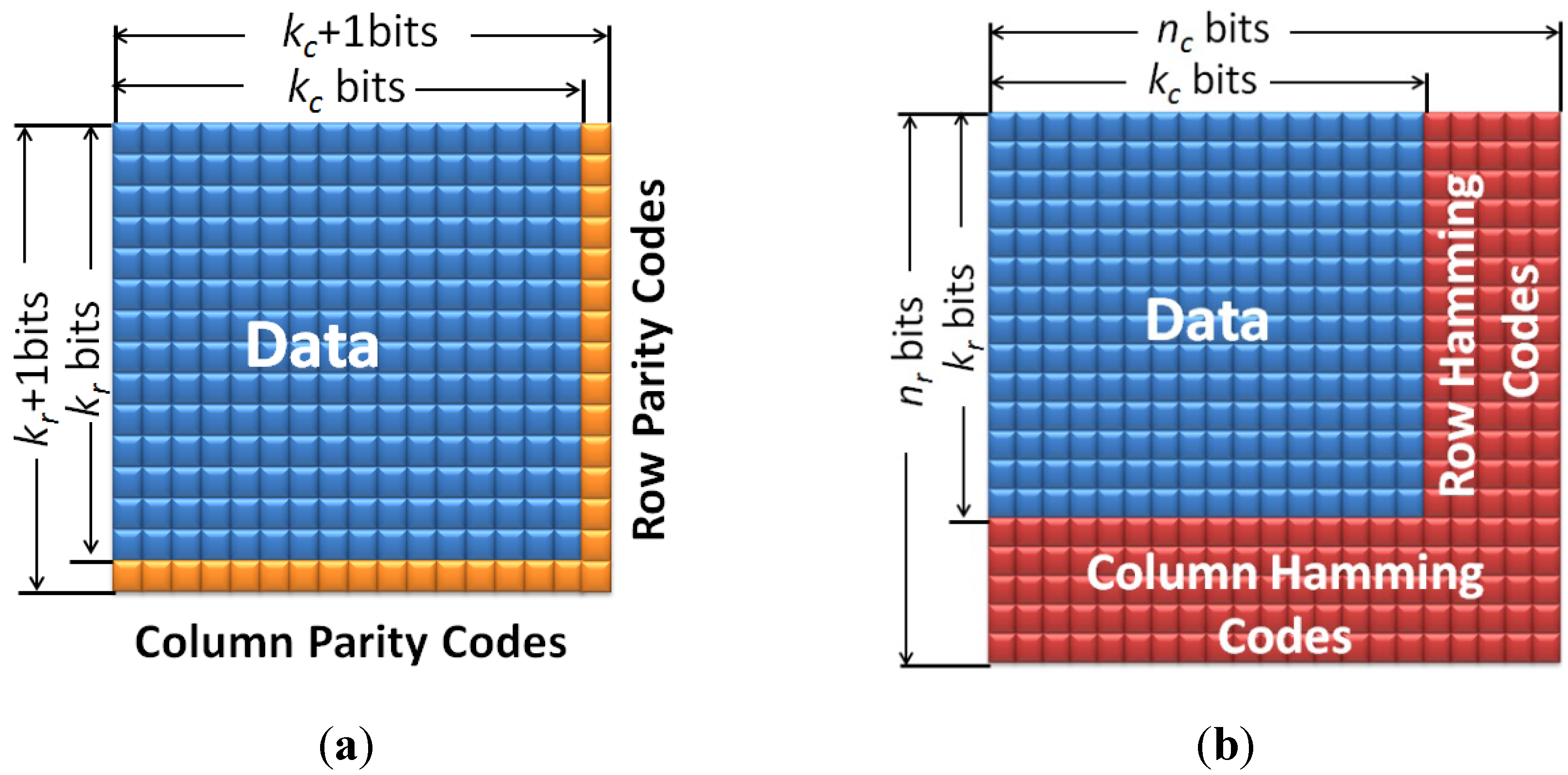
For rectangular codes, k-bit data within one cache line is first divided into kr rows and kc columns (as shown in Figure 1a). For each of kr rows, a row-direction parity check bit is added to detect single errors in the row; similarly, for each of kc columns, a column-direction parity check bit is used to detect single errors in the column; the bottom right corner can be either the column parity check bit or the row parity check bit. Therefore, the code word length for k bits data is n = (k + kr + kc + 1), and the code rate is k/n = k/(k + kr + kc + 1). For example, supposing that each cache line has 1024-bit data: d0, d1, …, d1023. For rectangular codes, we add one row parity bit r0 for d0, d1, d2, …, d31, add one row parity bit r1 for d32, d33, d34, …, d63, and so on. Similarly, we add one column parity bit c0 for d0, d32, d64, …, d992, add one column parity bit c1 for d1, d33, d65, …, d993, and so on. Finally, we will add one extra check-on-check bit c. Then, we will store all these data and check bits in the following one-dimensional way: d0, d1, d2, …, d31, r0, d32, d33, d34, …, d63, r1, …, d992, d993, d994, …, d1023, r31, c0, c1, … , c32, c.
Figure 1. (a) Rectangular codes, and (b) Hamming product codes.
Jlpea 04 00044 g001
The rectangular code has the minimal Hamming distance of four, and therefore can correct single errors and detect double errors. However, in our work, we do not use the rectangular codes’ error correction capability. Instead, we only use the rectangular code to detect cache errors. Therefore, the rectangular code can detect three random errors; meanwhile, the rectangular code can detect single burst errors with any length as we will prove later, and it can also detect error patterns in which there is at least one row/column with an odd number of errors.

3.2. Hamming Product Codes

Similar to rectangular codes, Hamming product codes also first divide k-bits data into kr rows and kc columns (as shown in Figure 1b). For each of kr rows, (nckc) row-direction Hamming check bits are added to correct single errors in the row; for each of the kc columns, (nrkr) column-direction Hamming check bits are used to correct single errors in the column; the bottom right corner can be either column- or row-direction Hamming check bits. Therefore, the code word length for k bits data is n = nr×nc, and the code rate is k/n = k/(nr + nc).
In theory, Hamming product codes have a minimal Hamming distance of 16, and therefore can correct seven errors and detect eight errors. However, in our work, we use the following three-stage decoding process, which is similar to [29], to correct errors at a low latency cost: Stage 1, correct single error in each row; Stage 2, correct single error in each column; and Stage 3, correct single error in each row again after Stage 1 and Stage 2 have corrected parts of the errors.
Table 1 shows the check bits overheads and the maximal code rates achieved by rectangular code and Hamming product code. Taking 1024-bit cache line as example, rectangular codes only require 64 check bits, while Hamming product codes need 384 check bits. Meanwhile, the code rates of rectangular codes and Hamming product codes are 94.1% and 72.8%, respectively. It is clear that rectangular codes introduce a much higher code rate than Hamming product codes. Also, the encoding and decoding process for rectangular codes is pretty simple because it only consists of several XOR operations. Thus, rectangular codes can minimize encoding/decoding latency and power overhead. However, rectangular codes can only provide a limited error correction capability. In contrast, Hamming product codes obtain a high error correction capability at the cost of large storage overhead, high latency, and power overhead. This comparison between rectangular and Hamming product code motivates the proposed two-layer ECCs.
Table 1. Code rate comparison between rectangular codes and Hamming product codes (HPC).
Cache Line SizencnrRectangular Check BitsRectangular Code RateHPC Check BitsHPC Code Rate
1024-bit cache line32326494.1%38472.8%
512-bit cache line32164891.4%25666.7%
256-bit cache line16163288.9%16061.5%%

3.3. Two-Layer ECC Combining Rectangular and Hamming Product Codes
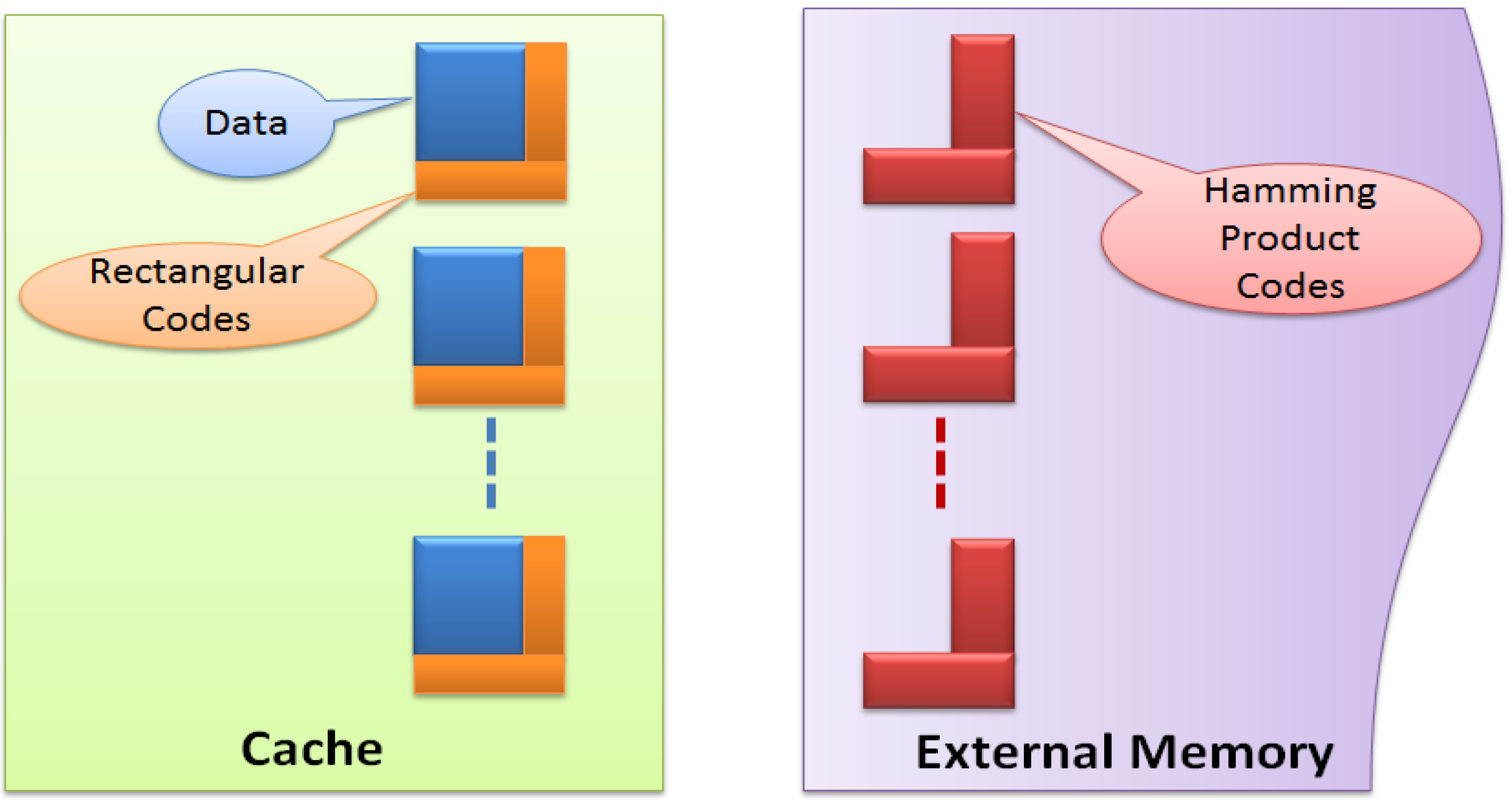
Rectangular codes enable fast error detection with low latency, power and storage overhead, but are ineffective to correct multiple errors, while Hamming product codes can obtain a high error correction capability at the cost of high latency, large storage and power overhead. Therefore, we propose two-layer ECCs, which utilize the error detection capability of rectangular codes to detect errors, and the use error correction capability of Hamming codes to correct errors detected by rectangular codes. As shown in Figure 2, we employ rectangular codes for every cache line to detect errors. Once errors have been detected, they can be corrected by Hamming product codes or loading replication from external memory depending on whether the related cache line is dirty or not. Also, Hamming product codes need to be updated when necessary.
Figure 2. Two-layer error control codes (ECC) combining rectangular and Hamming product codes.
Jlpea 04 00044 g002
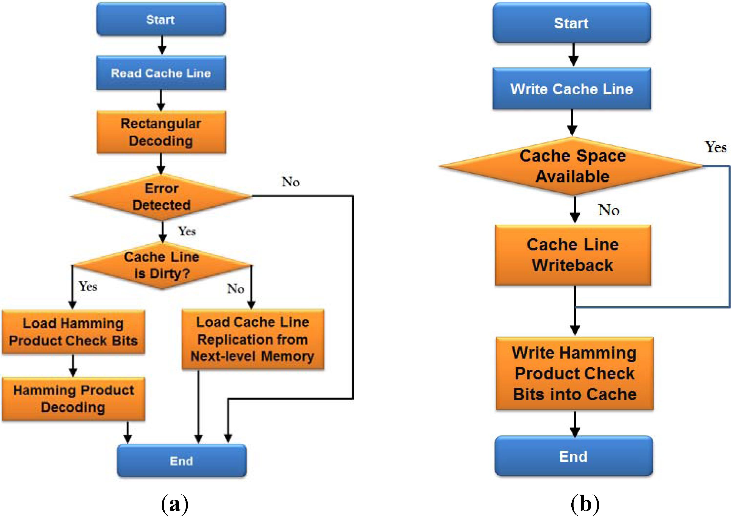
Figure 3 shows a flow chart of cache line read and write operations using the proposed two-layer ECCs. In the case of cache line read, a conventional cache line read operation is first performed. Then, fast rectangular decoding, which only consists of several XOR operations, is conducted to detect errors. If there are errors detected by rectangular decoding, we need to check whether the related cache line is dirty or not. If the related cache line is clean, we simply load data replication from the next-level memory because a clean cache line means that the newest data replication is in the next-level memory; if the related cache line is dirty, we need to load Hamming product check bits. Then, Hamming product decoding is performed to correct errors detected by rectangular decoding. In the case of cache line write, a conventional cache line write is first performed. Then, we need also write Hamming product check bits, and cache line write back might be performed if necessary.
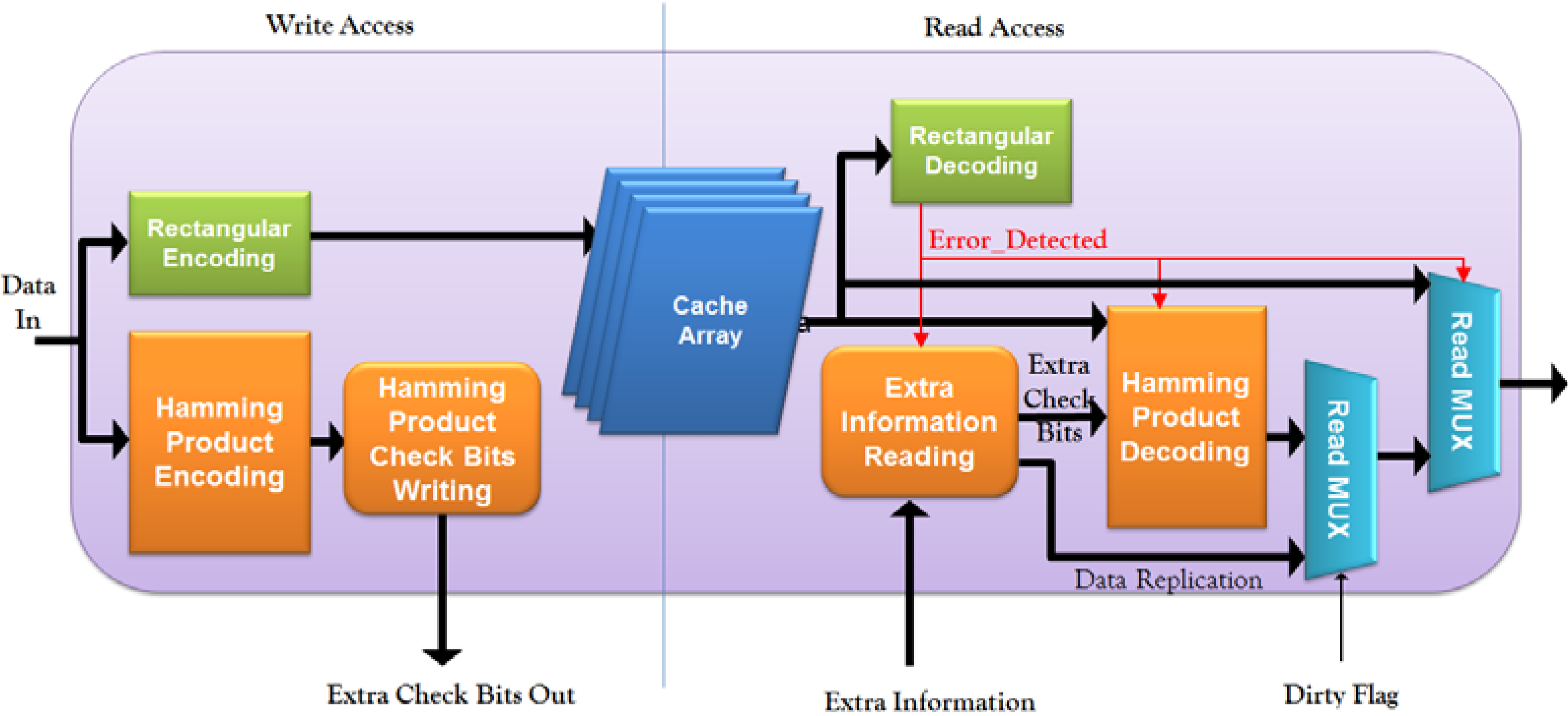
Figure 4 shows cache architecture using the proposed approach. In cache write port, rectangular encoding is performed to generate rectangular check bits for each cache line. These rectangular check bits, together with the original data, are stored in the cache array. Meanwhile, Hamming product check bits are also calculated using the Hamming Product Encoding module, and written into the memory hierarchy with the Hamming Product Check Bits Writing module. In cache read port, rectangular decoding is first performed to check whether there are errors in the cache line or not. If there is no error, the data will go directly through the Read MUX module; if there is an error detected by rectangular decoding, extra Hamming product check bits or data replication will be read from the memory hierarchy depending on whether the related dirty flag is set or not.
Figure 3. Flow chart of (a) Cache line read, and (b) Cache line write of proposed approach.
Jlpea 04 00044 g003
Figure 4. Cache achitecture using proposed approach.
Jlpea 04 00044 g004

4. Analysis and Experimental Results

In this section, we compare the proposed two-layer ECCs with different fault-tolerant methods in terms of reliability, storage overhead, performance degradation by analysis and experiments. In detail, we compare the proposed method with the following techniques:
  • 16-way SECDED: 16 interleaved SECDED codes are applied for every cache line;
  • 8-way SECDED: 8 interleaved SECDED codes are applied for every cache line;
  • 8-way DECTED: 8 interleaved DECTED codes are applied for every cache line;
  • 4-way DECTED: 4 interleaved DECTED codes are applied for every cache line;
  • 4-way 4EC5ED: 4 interleaved 4EC5ED codes are applied for every cache line;
  • 2-way 4EC5ED: 2 interleaved 4EC5ED codes are applied for every cache line.

4.1. Experimental Setup

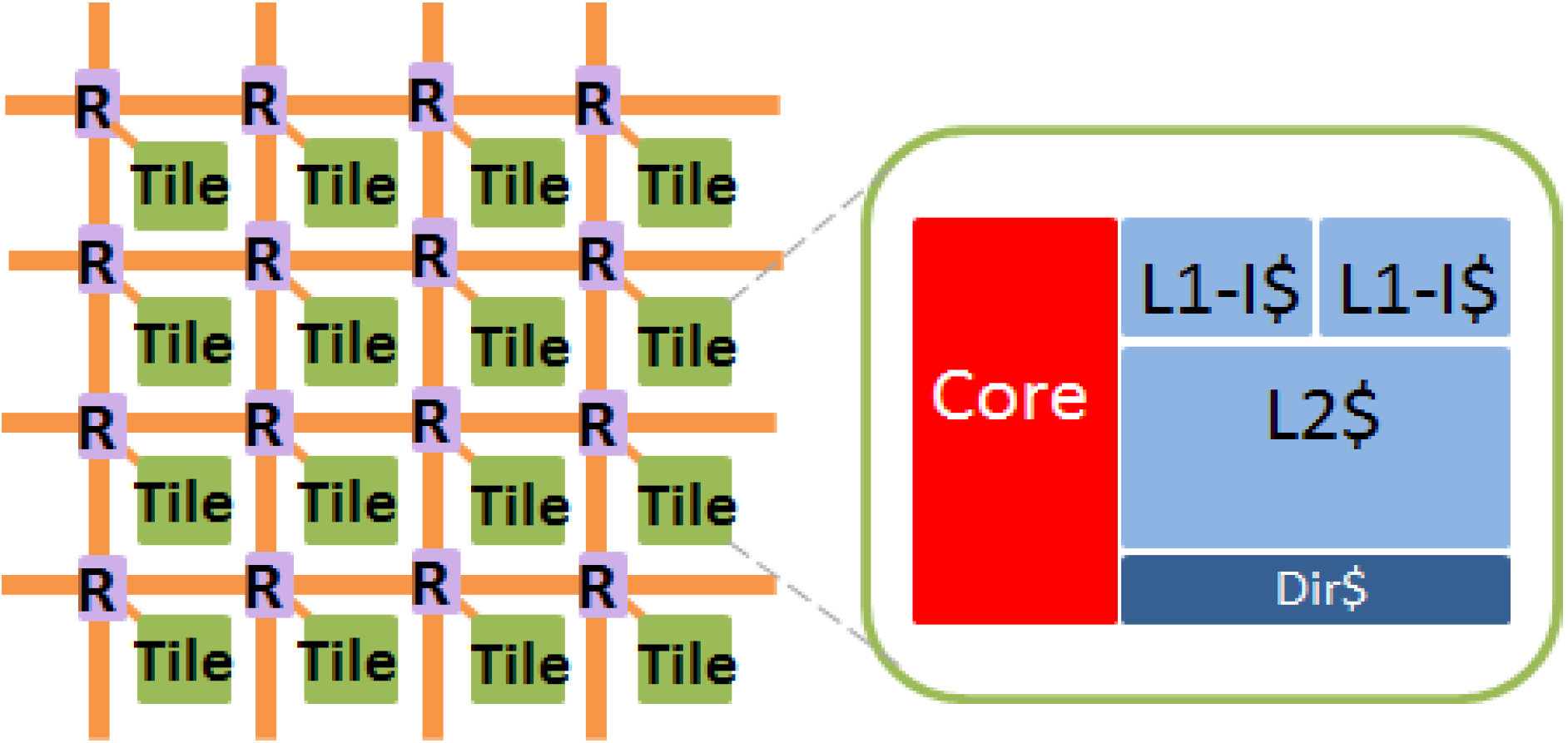
Our evaluation is based on a 1024-tile many-core system using 11 nm predictive tri-gate technology [30]. Each tile consists of a single-issue 64-bit core, four-way 32KB private L1 instruction cache, four-way 32KB private L1 data cache, and eight-way 256KB private L2 cache (Table 2 and Figure 5 A mesh network-on-chip (NoC) with wormhole flow control is adopted. Least Recently Used (LRU) cache replacement policy is used for both L1 and L2 caches. To evaluate performance degradation, we use a parallel many-core simulator, Graphite [31], which integrates CACTI [32]. To evaluate cache reliability, C simulation models for cache with various fault-tolerant approaches and the proposed method are built.
Table 2. 1024-tile system parameter.
ParametersValue
Tile Number1024
Core Type64 bits single-issue
L1-I/L1-D Cache, Private
Cache Size32 kb
Associativity4
Replacement PolicyLRU
Tag Access Time1 cycle
Data Access Time1 cycle
L2 Cache, Private
Cache Size256 kb
Associativity8
Replacement PolicyLRU
Tag Access Time3 cycles
Data Access Time8 cycles
External Memory
Memory Access Time100 cycles
Figure 5. 1024-tile system architecture.
Jlpea 04 00044 g005

4.2. Burst Error Control Capability

There are two types of errors: burst errors and random errors. Here, we evaluate the burst error control capability. Random error will be evaluated in the next subsection. We make two claims related to burst error detection and correction capability of the two-layer ECCs. The proof is also given.
Claim 1: the proposed approach can detect single a burst error of any length.
Proof:
All data and check bits are stored in a one-dimensional way as presented in Section 3.1. There are two cases for any single burst error in this one-dimensional data and check bits: Case 1—the burst error spans at least one whole row, as shown in Figure 1, and Case 2—the burst error does not span one whole row.
For Case 1, the Row Parity Decoder for the row where all bits have errors will detect this burst error because nc is odd, and the parity codes can detect odd numbers of errors.
For Case 2, the fact that the burst error does not span any row means that there is at least one column containing one error. Otherwise, if all columns had two or more errors, there would be at least one whole row in which all bits had errors, which is in conflict with our precondition; if all columns had zero errors, there would be no burst error at all, which is also in conflict with our precondition; if some of the columns had two or more errors, while the rest had no error, then, there would be multiple burst errors, which is still in conflict with our precondition. Hence, for this case, at least one column has one error, and the related Column Parity Decoder can detect this burst error because the parity codes can detect one error. [Q.E.D.]
Claim 2: the proposed approach can correct single burst errors up to nc + 1 bits.
Proof:
For a burst error of nc + 1 bits, each column in Figure 1 has 1 error at most except for one, which has two errors. Otherwise, if two of the columns had two or more errors, this burst error would have at least nc + 2 bits. Therefore, the Column SECDED Decoders can correct all errors except those in the column with two errors. Then, the Row SECDED Decoder at Stage 3 can correct this column. Thus, the proposed approach can correct single burst errors up to nc + 1 bits. [Q.E.D.]
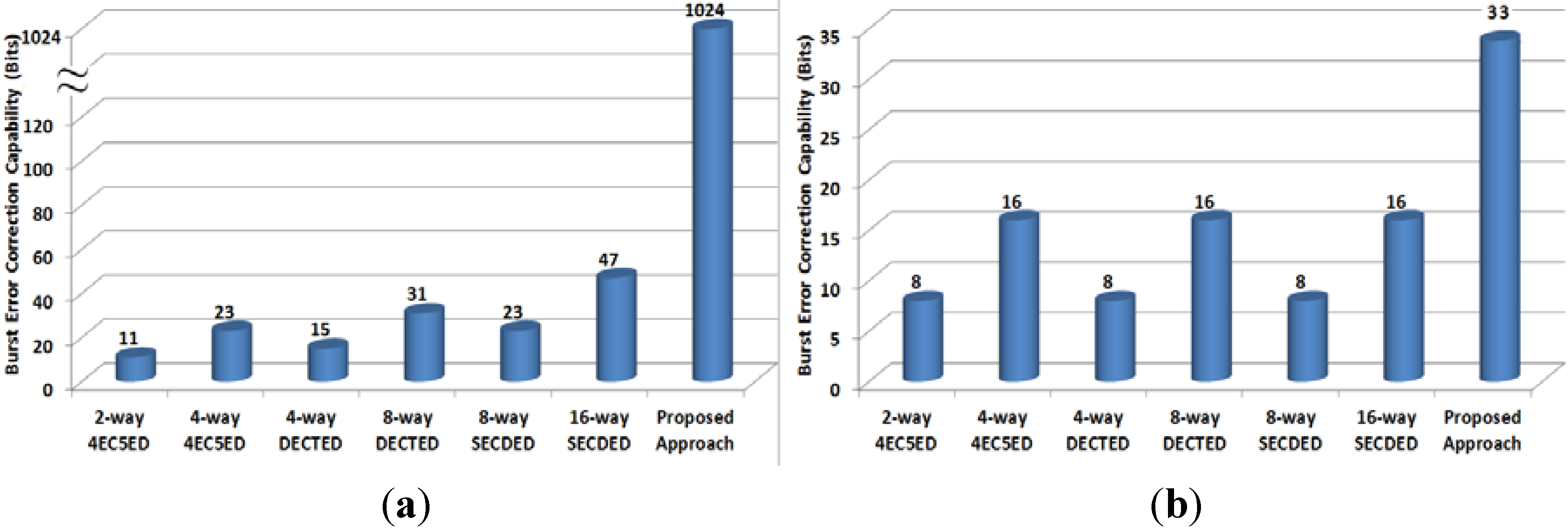
SECDED can correct a single error and detect double errors. Therefore, 16-way SECDED can correct up to 16-bit burst errors. Here, we claim that 16-way SECDED can detect up to 47-bit burst errors instead of 32-bit burst errors. The reason for this is that for the 16-way SECDED, at least one of SECDED ways will have no more than a two-bit error in the case of a 47-bit burst error (If all 16 SECDED ways had more than a two-bit error, there would be at least a 3 × 16 = 48 bits burst error). Therefore, at least one of SECDED will report an error in the case of a 47-bits burst error.
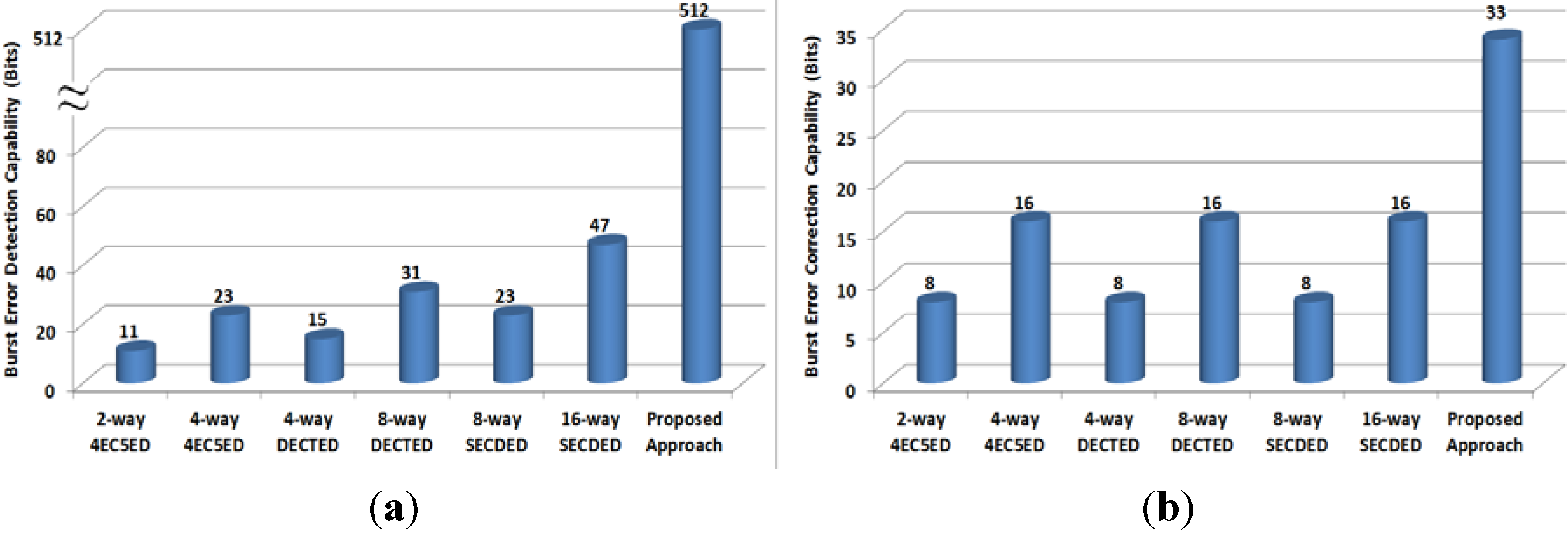
Similarly, 8-way SECDED can correct up to 8-bit burst errors, and detect up to 23-bit burst errors; 8-way DECTED can correct up to 16-bit burst errors, and detect up to 31-bit burst errors; 4-way DECTED can correct up to 8-bit burst errors, and detect up to 15-bit burst errors; 4-way 4EC5ED can correct up to 16-bit burst errors, and detect up to 23-bit burst errors; and, 2-way 4EC5ED can correct up to 8-bit burst error, and detect up to 11-bit burst error.
Figure 6 and Figure 7 show the error detection and correction capabilities of various fault-tolerant methods for 1024-bit and 512-bit cache lines, respectively. In the case of 1024-bit cache line, we set kc = kr = 32 to achieve minimal storage overhead; and in the case of 512-bit cache line, we set kc = 32, and kr = 16 for the same goal. The proposed approach can achieve the highest burst error detection and correction capability. If we take a 1024-bit cache line as example, the proposed approach can detect a 1024-bit burst error, which is 22×, 45×, 33×, 68×, 45×, 93× that achieved by 16-way SECDED, 8-way SECDED, 8-way DECTED, 4-way DECTED, 4-way 4EC5ED and 2-way 4EC5ED, respectively. Meanwhile, the proposed approach can correct 33-bit burst errors, which is 4.1×, 2.1×, 4.1×, 2.1×, 4.1×, 2.1× of that achieved by 16-way SECDED, 8-way SECDED, 8-way DECTED, 4-way DECTED, 4-way 4EC5ED and 2-way 4EC5ED, respectively.
Figure 6. Burst error (a) detection capability; and (b) correction capability (1024-bit cache line).
Jlpea 04 00044 g006
Figure 7. Burst error (a) detection capability, and (b) correction capability (512-bit cache line).
Jlpea 04 00044 g007

4.3. Mean-Error-to-Failure Evaluation

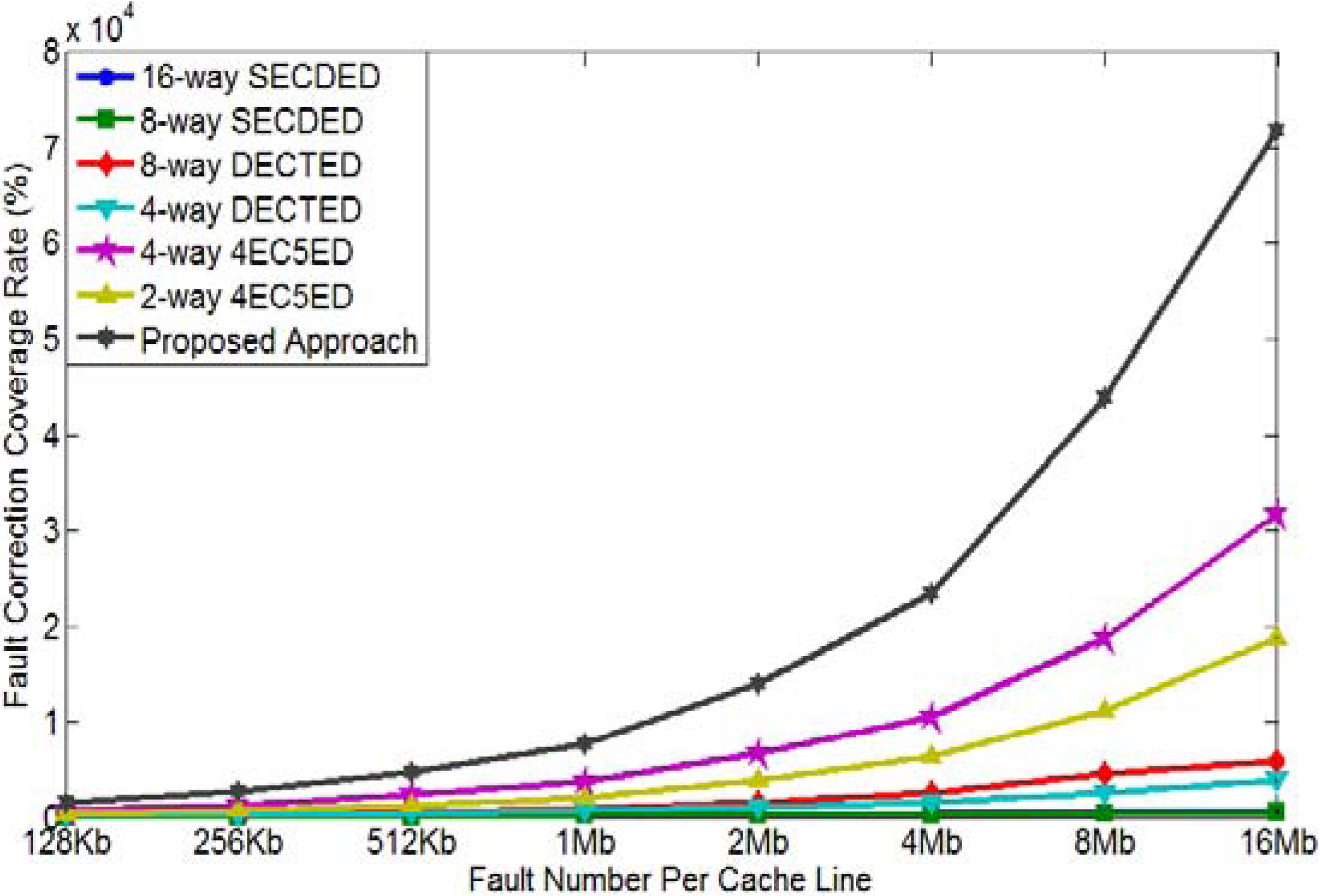
In this subsection and the following one, we evaluate the random error control capability. Mean-error-to-failure (METF), which represents the average number of errors that cause failure of the whole cache system, and Mean-time-to-failure (MTTF), which represents the average time before reaching cache failure, are two metrics to evaluate system reliability. In this section, we evaluate METF of various cache error management solutions. C simulation models for cache systems with various fault-tolerant methods are built. Our simulations run for various cache sizes, such as 128 kb, 512 kb, 1 Mb, 2 Mb, 4 Mb, 8 Mb and 16 Mb. For each cache size, 1000 simulations are tested.
Figure 8 plots METF results achieved with our simulation for 1024-bit cache line. As shown in the figure, the proposed approach achieves the highest METF, which means our solution can tolerate the most errors. For example, METF of the proposed approach for 16 Mb cache is 5.43 × 10⁴, while METF of 16-way SECDED, 8-way SECDED, 8-way DECTED, 4-way DECTED, 4-way 4EC5ED, and 2-way 4EC5ED are 562, 442, 3.84 × 10³, 3.12 × 10³, 1.76 × 10⁴, and 1.08 × 10⁴, respectively. The proposed two-layer ECCs can improve METF by 96×, 123×, 14×, 17×, 3× and 5×, respectively. Even for a cache size of 128 kb, the proposed approach provides METF of 1241, while 16-way SECDED, 8-way SECDED, 8-way DECTED, 4-way DECTED, 4-way 4EC5ED, and 2-way 4EC5ED only obtain METF of 56, 41, 183, 112, 44 and 206 respectively. The proposed two-layer ECCs can improve METF by 22×, 30×, 6.8×, 11×, 2.8×, and 6.0×, respectively.
Figure 9 plots METF results achieved by our simulation for 512-bit cache line. As shown in the figure, the proposed approach achieves the highest METF, which means our solution can tolerate the most errors. For example, METF of the proposed approach for 16Mb cache is 7.18 × 10⁴, while METF of 16-way SECDED, 8-way SECDED, 8-way DECTED, 4-way DECTED, 4-way 4EC5ED, and 2-way 4EC5ED are 629, 538, 5.91 × 10³, 3.89 × 10³, 3.16 × 10⁴, and 1.87 × 10⁴, respectively. The proposed two-layer ECCs can improve METF by 114×, 133×, 12×, 18×, 2.3× and 3.8×, respectively. Even for a cache size of 128 kb, the proposed approach provides METF of 1507, while 16-way SECDED, 8-way SECDED, 8-way DECTED, 4-way DECTED, 4-way 4EC5ED, and 2-way 4EC5ED only obtain METF of 68, 53, 298, 178, 700 and 449, respectively. The proposed two-layer ECCs can improve METF by 22×, 28×, 5.1×, 8.5×, 2.2×, and 3.4×, respectively.
Figure 8. Mean-Error-to-Failure (METF) comparison (cache line size = 1024 bits).
Jlpea 04 00044 g008
Figure 9. METF comparison (cache line size = 512 bits).
Jlpea 04 00044 g009

4.4. Mean-Time-to-Failure Evaluation

The MTTF, which represents the average time before reaching the failure of a cache system, can be given using the following equation:
Jlpea 04 00044 i001
Figure 10 plots MTTF achieved by various approaches for 1024-bit cache line given a fault rate of 10−5/day and 10−4/day, respectively. As shown in the figure, the proposed approach can achieve the highest MTTF compared to all other approaches. For example, in the case of a 10−5/day fault rate, the proposed approach can correctly work for 947, 786, 762, 616, 481, 441, 408, and 323 days before reaching cache failure for cache sizes of 128 kb, 256 kb, 512 kb, 1 Mb, 2 Mb, 4 Mb, 8 Mb, and 16 MB, which are about 2.8×–3.3× those achieved by the next-best solution, the 4-way 4EC5ED. Even in the case of the high fault rate of 10−4/day, the proposed approach can still provide MTTF of 95, 79, 76, 62, 48, 44, 41, and 32 days for various cache sizes, while the next-best solution, 4-way 4EC5ED, can only achieve MTTF of 16, 13, 13, 12, 9.5, 9.5, 7.2 and 6.4 days, respectively.
Figure 11 plots MTTF achieved by various approaches for 512-bit cache line given fault rates of 10−5/day and 10−4/day, respectively. As shown in the figure, the proposed approach can achieve the highest MTTF compared to all other approaches. For example, in the case of a 10−5/day fault rate, the proposed approach can correctly work for 1150, 1024, 907, 727, 669, 556, 523, and 428 days before reaching cache failure for cache sizes of 128 kb, 256 kb, 512 kb, 1 Mb, 2 Mb, 4 Mb, 8 Mb, and 16 MB, which are about 2.0×–2.3× those achieved by next-best solution, the 4-way 4EC5ED. Even in the case of the high fault rate of 10−4/day, the proposed approach can still provide MTTF of 115, 102, 91, 73, 67, 56, 52 and 43 days for various cache sizes, while next-best solution, 4-way 4EC5ED, can only achieve MTTF of 34, 30, 24, 20, 19, 15, 13 and 11 days, respectively.
Figure 10. METF comparison (a) Cache line size = 1024 bits, fault rate 10−5/day; and (b) Cache line size = 1024 bits, fault rate 10−4/day.
Jlpea 04 00044 g010
Figure 11. METF comparison (a) Cache line size = 512 bits, fault rate 10−5/day, and (b) Cache line size = 512 bits, fault rate 10−4/day.
Jlpea 04 00044 g011

4.5. Overhead Evaluation

Various cache error management approaches introduce redundant check parity bits, which introduce extra storage overhead into cache. Here, we evaluate storage overhead required by the proposed approach and other solutions. t-bit error correction codes require t × m check bits, and t-bit error correction and (t + 1) detection codes require t × m + 1 check bits, where m is the smallest possible integer which meets the requirement (k + t × m + 1) < 2m. Therefore, SECDED requires 9, 8, and 7 check bits for data lengths of 128, 64 and 32 bits; DECTED requires 19, 17, and 15 check bits for data lengths of 256, 128 and 64 bits; and 4EC5ED requires 41, 37 and 33 check bits for data lengths of 512, 256 and 128 bits. In addition, SEC requires six and five bits for data lengths of 32 and 16 bits, and the parity code requires 1 bit for any data length. Based on this information, we can evaluate the storage overhead of various cache error control methods.
Table 3(a) shows the comparison of storage overhead between various cache fault-tolerant methods and the proposed approach for 1024-bit cache line. Here, the proposed approach introduces a 64-bit storage overhead for each cache line, while 16-way SECDED, 8-way SECDED, 8-way DECTED, 4-way DECTED, 4-way 4EC5ED, and 2-way 4EC5ED lead to storage overheads of 128 bits, 72 bits, 136 bits, 76 bits, 148 bits and 84 bits, respectively. Therefore, the proposed approach can reduce the storage overhead by 70%, 11%, 53%, 18%, 57%, and 24%, respectively. Table 3(b) shows the comparison of storage overheads for a 512-bit cache line, and the proposed approach still introduces the least storage overhead.
Table 3. Overhead evaluation. (a) 1024-bit cache line; (b) 512-bit cache line.
(a)Data/ WayCheck bits/Way#Way#Total bits(b)Data/ WayCheck bits/Way#Way#Total bits
16-way SECDED6481612816-way SECDED32716112
8-way SECDED12898728-way SECDED64884
8-way DECTED1281781368-way DECTED64158120
4-way DECTED256194764-way DECTED12817468
4-way 4EC5ED2563741484-way 4EC5ED128334132
2-way 4EC5ED512412842-way 4EC5ED25637274
Proposed***64Proposed***48

4.6. Performance Degradation

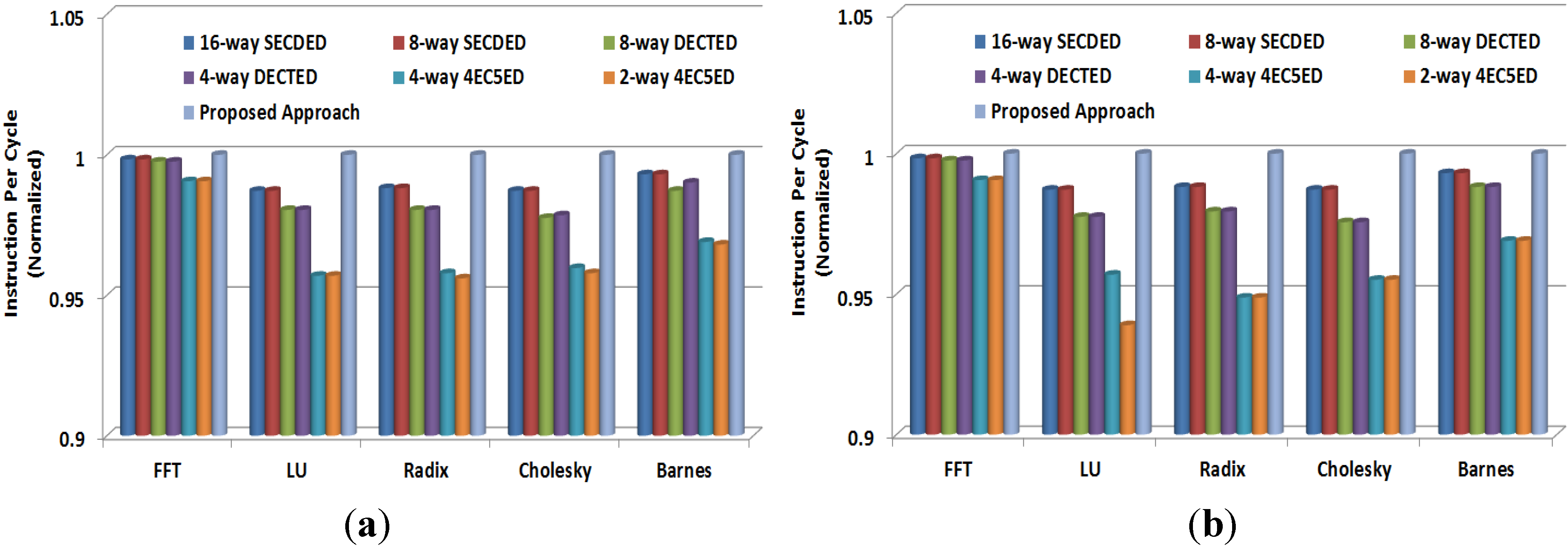
Various fault-tolerant approaches can increase cache access time because of the introduction of a ECC encoder/decoder. Additionally, the proposed approach can possibly increase next-level memory access numbers although the latency of the parity code, which is adopted by the proposed approach, is trivial. Therefore, fault-tolerant approaches can degrade system performance to some extent. In order to evaluate system performance, instruction per-cycle (IPC) for cache line sizes of 1024 bits and 512 bits are plotted in Figure 12. In our evaluation, we add zero cycle latency for parity code, one cycle latency for SECDED, two cycle latencies for DECTED, and seven cycle latencies for 4EC5ED [23,33]. As shown in the figure, the proposed two-layer ECCs achieves similar IPC with 8-way SECDED and 16-way SECDED because the two-layer ECCs only requires simple parity code encoding / decoding processes for most cache accesses. All other approaches, including the 8-way DECTED, 4-way DECTED, 4-way 4EC5ED, and 2-way 4EC5ED, obtain less IPC because they require complex DECTED or 4EC5ED encoding/decoding processes. Especially, the 4-way 4EC5ED and 2-way 4EC5ED, which introduce high latencies to every cache access, can degrade system IPC. For instance, 8-way 4EC5ED and 4-way 4EC5ED provide a 1.1%–7.2% lower IPC than the proposed approach for different SPLASH2 benchmarks, including FFT, LU, Radix, Cholesky and Barnes, when cache line size is 1024 bits.
Figure 12. Instruction per cycle (IPC) (a) 1024-bit cache line, and (b) 512-bit cache line.
Jlpea 04 00044 g012

5. Conclusions

As technology improves, high reliability and low cost cache fault-tolerant approaches are required to ensure reliable systems while meeting strict budgets of area and latency overheads. In this paper, we propose a novel two-layer ECCs combining rectangular and Hamming product codes in an efficient way to address cache error for high error rate while reducing area and latency overhead. Our experimental results show that the proposed approach can improve METF and MTTF up to 2.8×, reduce storage overhead by over 57%, and increase IPC by to 7% compared to the 4-way 4EC5ED code, which belongs to the high reliability and high cost ECC codes. Additionally, the proposed approach can increase METF and MTTF up to 133×, reduce storage overhead by over 11%, and achieve a similar IPC degradation compared to the 8-way SECDED code, which belongs to the group of low reliability and low cost codes. Our future work is to minimize the memory access overhead introduced by the proposed approach.

References

  1. Agostinelli, M.; Hicks, J.; Xu, J.; Woolery, B.; Mistry, K.; Zhang, K.; Jacobs, S.; Jopling, J.; Yang, W.; Lee, B.; et al. Erratic Fluctuations of SRAM Cache Vmin at the 90 nm Process Technology Node. In Proceedings of the IEEE International Electron Devices Meeting, IEDM Technical Digest, Washington, DC, USA, 5–7 December 2005.
  2. Borkar, S. Designing reliable systems from unreliable components: The challenges of transistor variability and degradation. IEEE Micro 2005, 25, 10–17. [Google Scholar] [CrossRef]
  3. Ruckerbauer, F.X.; Georgakos, X. Soft Error Rates in 65 nm SRAMs—Analysis of New Phenomena. In Proceedings of the IEEE International On-Line Testing Symposium (IOLTS), Crete, Greece, 8–11 July 2007; pp. 203–204.
  4. Zhang, M.; Ampadu, P. Variation-Tolerant Cache by Two-Layer Error Control Codes. In Proceedings of the 2013 IEEE International Symposium on Defect and Fault Tolerance in VLSI and Nanotechnology Systems (DFT), New York, NY, USA, 2–4 October 2013; pp. 161–166.
  5. Yoon, D.H.; Erez, M. Memory Mapped ECC: Low-Cost Error Protection for Last Level Caches. In Proceedings of the 36th International Symposium on Computer Architecture (ISCA-36), Austin, TX, USA, 20–24 June 2009; pp. 116–127.
  6. Reick, K.; Sanda, P.N.; Swaney, S.; Kellington, J.W.; Mack, M.J.; Floyd, M.S.; Henderson, D. Fault-Tolerant Design of the IBM Power6 Microprocessor. IEEE Micro 2008, 28, 30–38. [Google Scholar] [CrossRef]
  7. Chishti, Z.; Alameldeen, A.R.; Wilkerson, C.; Wu, W.; Lu, S.-L. Improving Cache Lifetime Reliability at Ultra-Low Voltages. In Proceedings of the International Symposium on Microarchitecture, New York, NY, USA, 12–16 December 2009; pp. 89–99.
  8. Wilkerson, C.; Alameldeen, A.R.; Chishti, Z.; Wu, W.; Somasekhar, D.; Lu, S.-L. Reducing Cache Power with Low-Cost, Multi-bit Error-Correcting Codes. In Proceedings of the International Symposium on Computer Architecture (ISCA), Saint-Malo, France, 19–23 June 2010.
  9. Radaelli, D.; Puchner, H.; Wong, S.; Daniel, S. Investigation of multi-bit upsets in a 150 nm technology SRAM device. IEEE Trans. Nucl. Sci. 2005, 52, 2433–2437. [Google Scholar] [CrossRef]
  10. Baeg, S.; Wen, S.; Wong, R. SRAM Interleaving distance selection with a soft error failure model. IEEE Trans. Nucl. Sci. 2009, 56, 2111–2118. [Google Scholar] [CrossRef]
  11. Kim, J.; Hardavellas, N.; Mai, K.; Falsafi, B.; Hoe, J.C. Multi-bit Error Tolerant Caches Using Two-Dimensional Error Coding. In Proceedings of the 40th International Symposium on Micro-architecture (Micro-40), Chicago, IL, USA, 1–5 December 2007.
  12. Argyrides, C.; Pradhan, D.K.; Kocak, T. Matrix codes for reliable and cost efficient memory chips. IEEE Trans. Very Large Scale Integr. (VLSI) Syst. 2011, 19, 420–428. [Google Scholar] [CrossRef]
  13. Wang, S.; Hu, J.; Ziavras, S.G. Replicating tag entries for reliability enhancement in cache tag arrays. IEEE Trans. Very Large Scale Integr. (VLSI) Syst. 2012, 20, 634–654. [Google Scholar]
  14. Kim, J.; Kim, S.; Lee, Y. SimTag: Exploiting Tag Bits Similarity to Improve the Reliability of the Data Caches. In Proceedings of the Conference on DesignAutomationand Test in Europe (DATE’10), Dresden, Germany, 8–12 March 2010; pp. 941–944.
  15. Wang, S. Characterizing System-Level Vulnerability for Instruction Caches against Soft Errors. In Proceedings of 2011 IEEE International Symposium on Defect and Fault Tolerance in VLSI and Nanotechnology Systems (DFT’11), Vancouver, Canada, 3–5 October2011; pp. 356–363.
  16. Schuster, S. Multiple word/bit line redundancy for semiconductor memories. IEEE J. Solid-State Circuits 1978, 13, 698–703. [Google Scholar] [CrossRef]
  17. Horiguchi, M. Redundancy Techniques for High-Density DRAMS. In Proceedings of the 2nd Annual IEEE International Conference Innovative Systems Silicon, Austin, TX, USA, 8–10 October 1997; pp. 22–29.
  18. Agarwal, A.; Paul, B.C.; Mahmoodi, H.; Datta, A.; Roy, K. A process-tolerant cache architecture for improved yield in nanoscale technologies. IEEE Trans. Very Large Scale Integr. (VLSI) Syst 2005, 13, 27–38. [Google Scholar] [CrossRef]
  19. Lee, H.; Cho, S.; Childers, B.R. Performance of Graceful Degradation for Cache faults. In Proceedings of the IEEE Computer Society Annual Symposium on VLSI (ISVLSI ’07), Porto Alegre, Brazil, 9–11 March 2007.
  20. Abella, J.;Carretero, J.; Chaparro, P.; Vera, X.; Gonzalez, A. Low Vccmin Fault-Tolerant Cache with Highly Predictable Performance. In Proceedings of the 42nd Annual IEEE/ACM International Symposium on Microarchitecture (MICRO’09), New York, NY, USA, 12–16 December 2009.
  21. Wilkerson, C.; Gao, H.; Alameldeen, A.R.; Chishti, Z.; Khellah, M.; Lu, S.-L. Trading off Cache Capacity for Reliability to Enable Low Voltage Operation. In Proceedings of the 35th International Symposium on Computer Architecture (ISCA’08), Beijing, China, 21–25 June 2008; pp. 203–214.
  22. Lu, S.-L.; Alameldeen, A.; Bowman, K.; Chishti, Z.; Wilkerson, C.; Wei, W. Architectural-Level Error-Tolerant Techniques for Low Supply Voltage Cache Operation. In Proceedings of the IEEE International Conference on IC Design & Technology (ICICDT’11), Kaohsiung, Taiwan, 2–4 May 2011.
  23. Aladmeldeen, A.; Wagner, I.; Chishti, Z.; Wu, W.; Wilkerson, C.; Lu, S.-L. Energy-Efficient Cache Design Using Variable-Strength Error-Correcting Codes. In Proceedings of the 38th International Symposium on Computer Architecture, San Jose, CA, USA, 4–8 June 2011.
  24. Zhang, M.; Stojanovic, V.M.; Ampadu, P. Reliable ultra-low-voltage cache design for many-core systems. IEEE Trans. Circuits Syst. II 2012, 59, 858–862. [Google Scholar] [CrossRef]
  25. Ampadu, P.; Zhang, M.; Stojanovic, V. Breaking the Energy Barrier in Fault-Tolerant Caches for Multicore Systems. In Proceedings of the Design, Automation & Test in Europe Conference & Exhibition, Grenoble, France, 18–22 March 2013; pp. 731–736.
  26. Li, C.; Zhang, M.; Ampadu, P. Reliable Ultra-Low Voltage Cache with Variation-Tolerance. In Proceedings of the IEEE 56th International Midwest Symposium on Circuits and Systems (MWSCAS), Columbus, OH, USA, 4–7 August 2013; pp. 121–124.
  27. Chang, L.; Fried, D.; Hergenrother, J.; Sleight, J.; Dennard, R.; Montoye, R.R.; Sekaric, L.; McNab, S.; Topol, W.; Adams, C.; et al. Stable SRAM Cell Design for the 32 nm Node and Beyond. In Proceedings of the 2005 Symposium on VLSI Technology, Digest of Technical Papers, Kyoto, Japan, 14–16 June 2005; pp. 128–129.
  28. Calhoun, B.H.; Chandrakasan, A. A 256 kb sub-threshold SRAM in 65 nm CMOS. IEEE J. Solid State Circuits 2007, 42, 680–688. [Google Scholar] [CrossRef]
  29. Fu, B.; Ampadu, P. On hamming product codes with type-II hybrid ARQ for on-chip interconnects. IEEE Trans. Circuits Syst. I 2009, 56, 2042–2054. [Google Scholar] [CrossRef]
  30. Kurian, G.; Chen, S.; Chen, C.-H.O.; Miller, J.E.; Michel, J.; Wei, L.; Antoniadis, D.A.; Peh, L.S.; Kimerling, L.; Stojanovic, V.; Agarwal, A. Cross-Layer Energy and Performance Evaluation of a Nanophotonic Manycore Processor System using Real Application Workloads. In Proceedings of the IEEE 26th International Parallel & Distributed Processing Symposium (IPDPS), Shanghai, China, 21–25 May 2012.
  31. Miller, J.; Kasture, H.; Kurian, G.; Gruenwald, C.; Beckmann, N.; Celio, C.; Eastep, J.; Agarwal, A. Graphite: A Distributed Parallel Simulator for Multicores. In Proceedings of the IEEE International Symposium on High Performance Computer Architecture (HPCA), Bangalore, India, 9–14 January 2009.
  32. Thoziyoor, S.; Ahn, J.; Monchiero, M.; Brockman, J.; Jouppi, N. A Comprehensive Memory Modeling Tool and its Application to the Design and Analysis of Future Memory Hierarchies. In Proceedings of the 35th International Symposium on Computer Architecture (ISCA), Beijing, China, 21–25 June 2008.
  33. Naseer, R.; Draper, J. Parallel Double Error Correcting Code Design to Mitigate Multi-Bit Upsets in SRAMs. In Proceedings of the 34th European Solid-State Circuits Conference (ESSCIRC), Edinburgh, UK, 15–19 September 2008; pp. 222–225.