
Graph Coloring via Locally-Active Memristor Oscillatory Networks

 ,
,  and
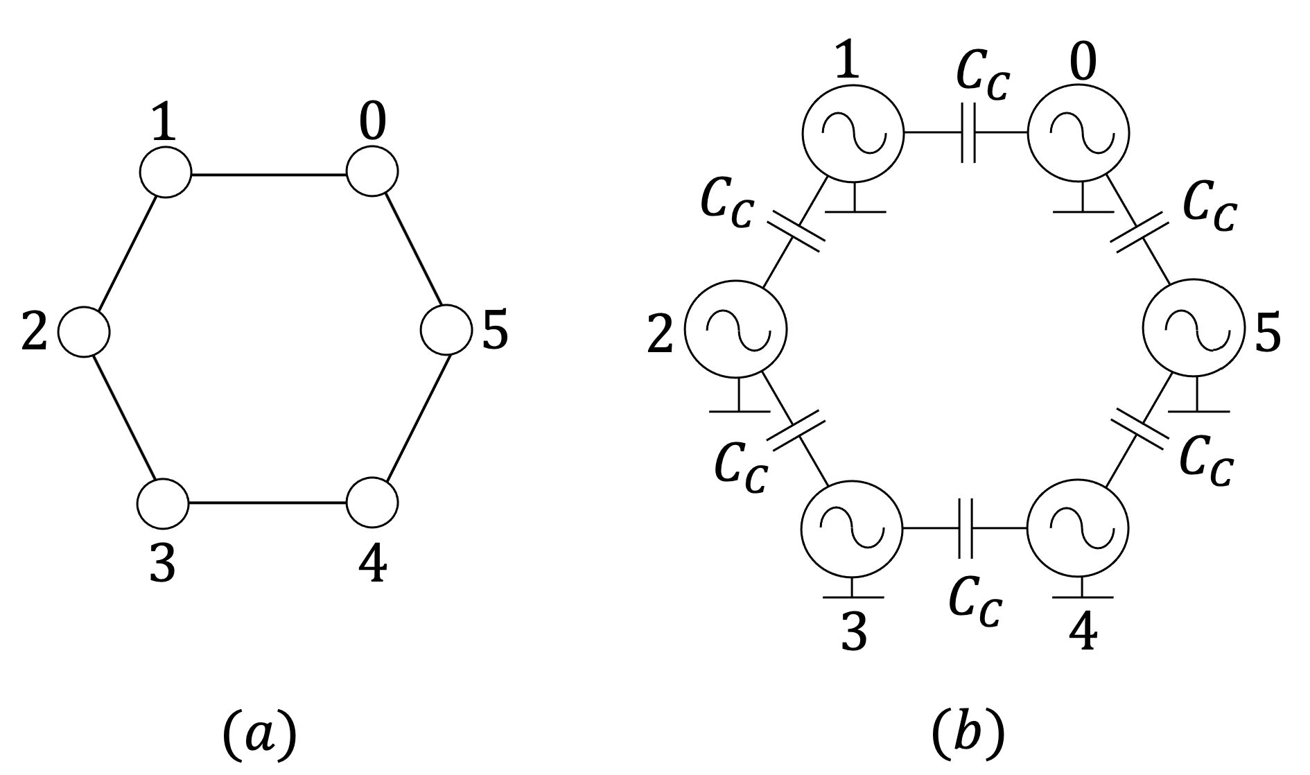
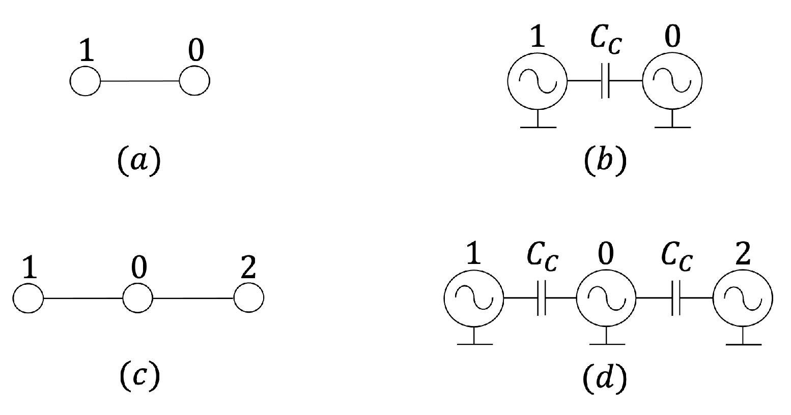
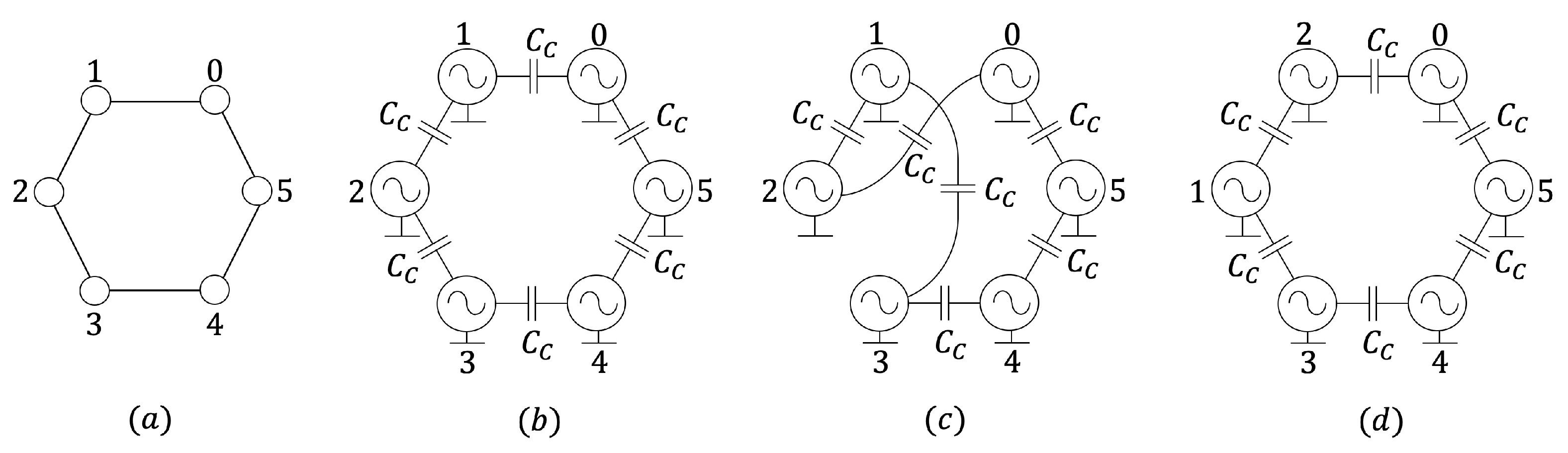
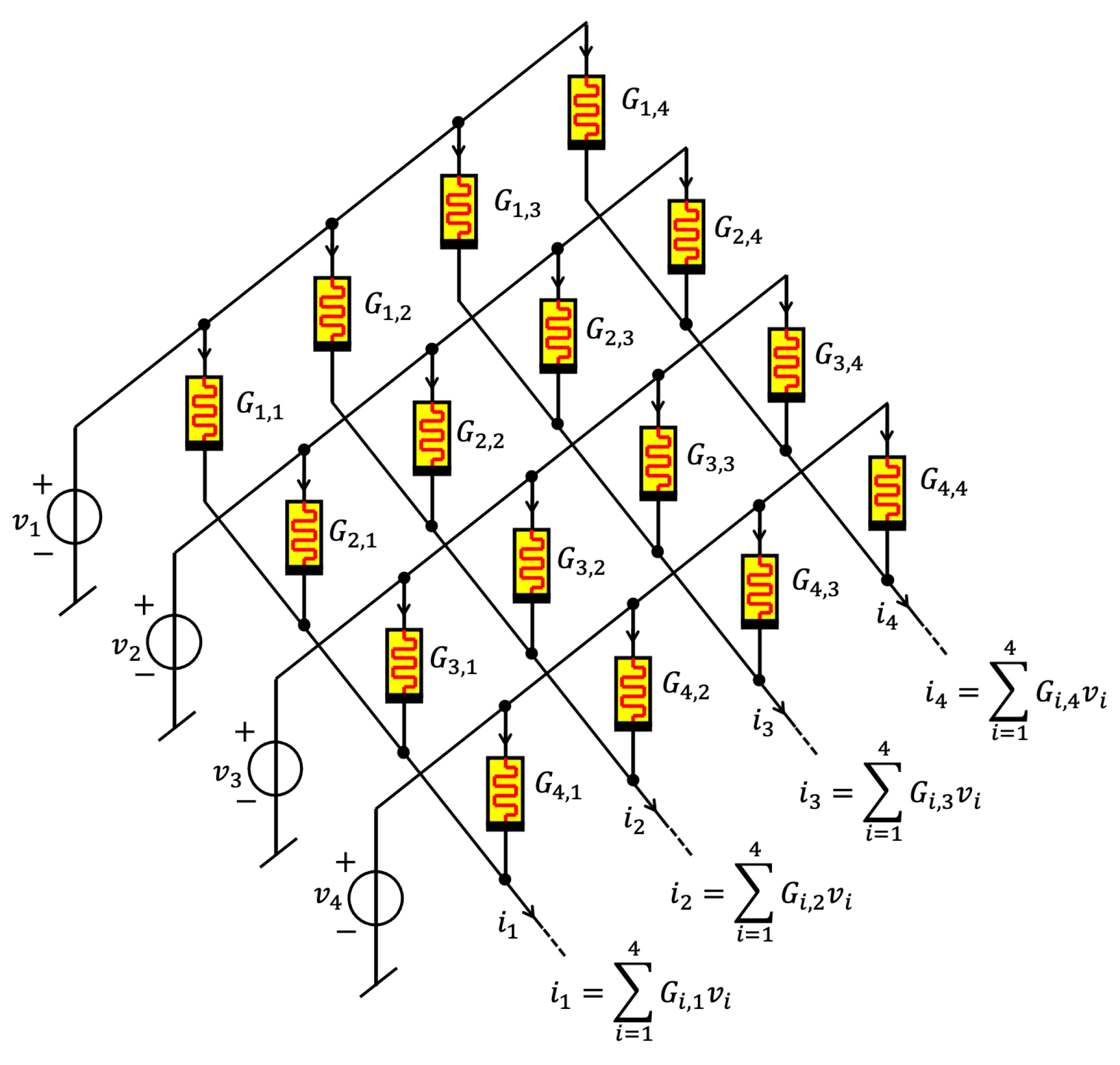
and 
Abstract
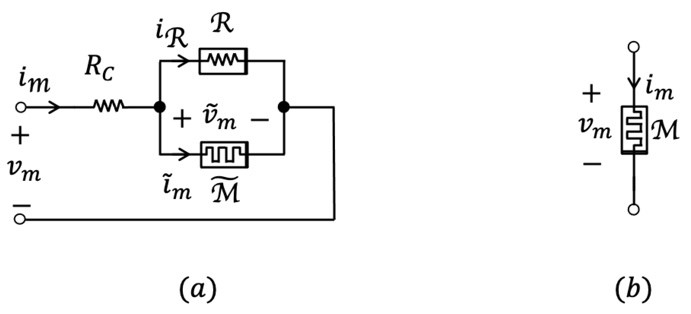
:1. Introduction
2. A Physics-Based Model for the Threshold Switching Dynamics of a Nano-Scale Locally-Active Memristor Device Stack
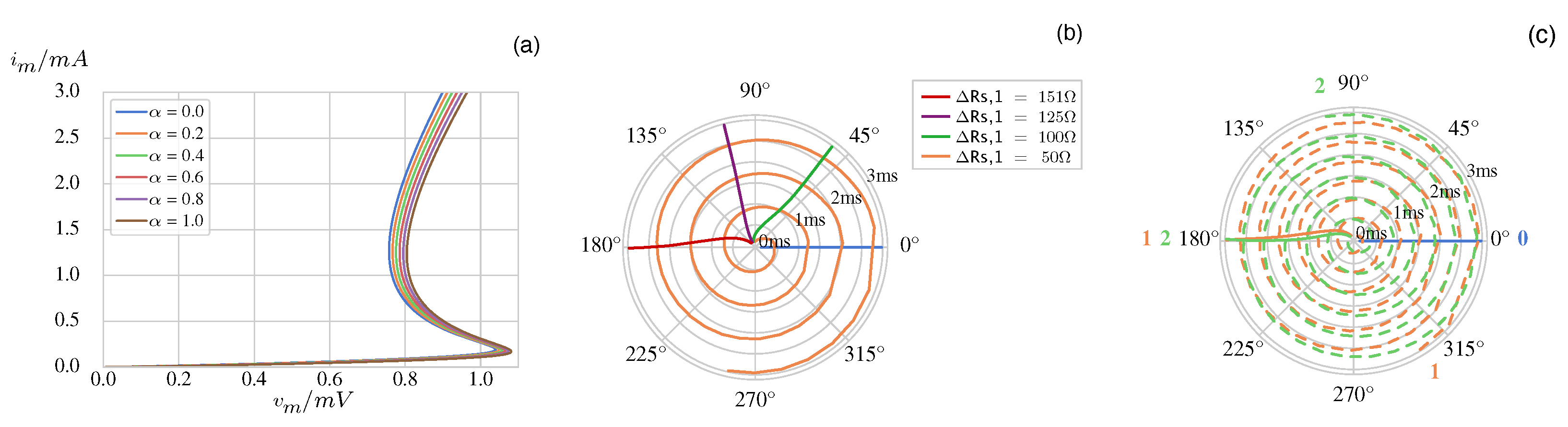
3. Memristive Computing Engine for Solving the Vertex Coloring Problem
3.1. Operating Principles of the Capacitively-Coupled Networks
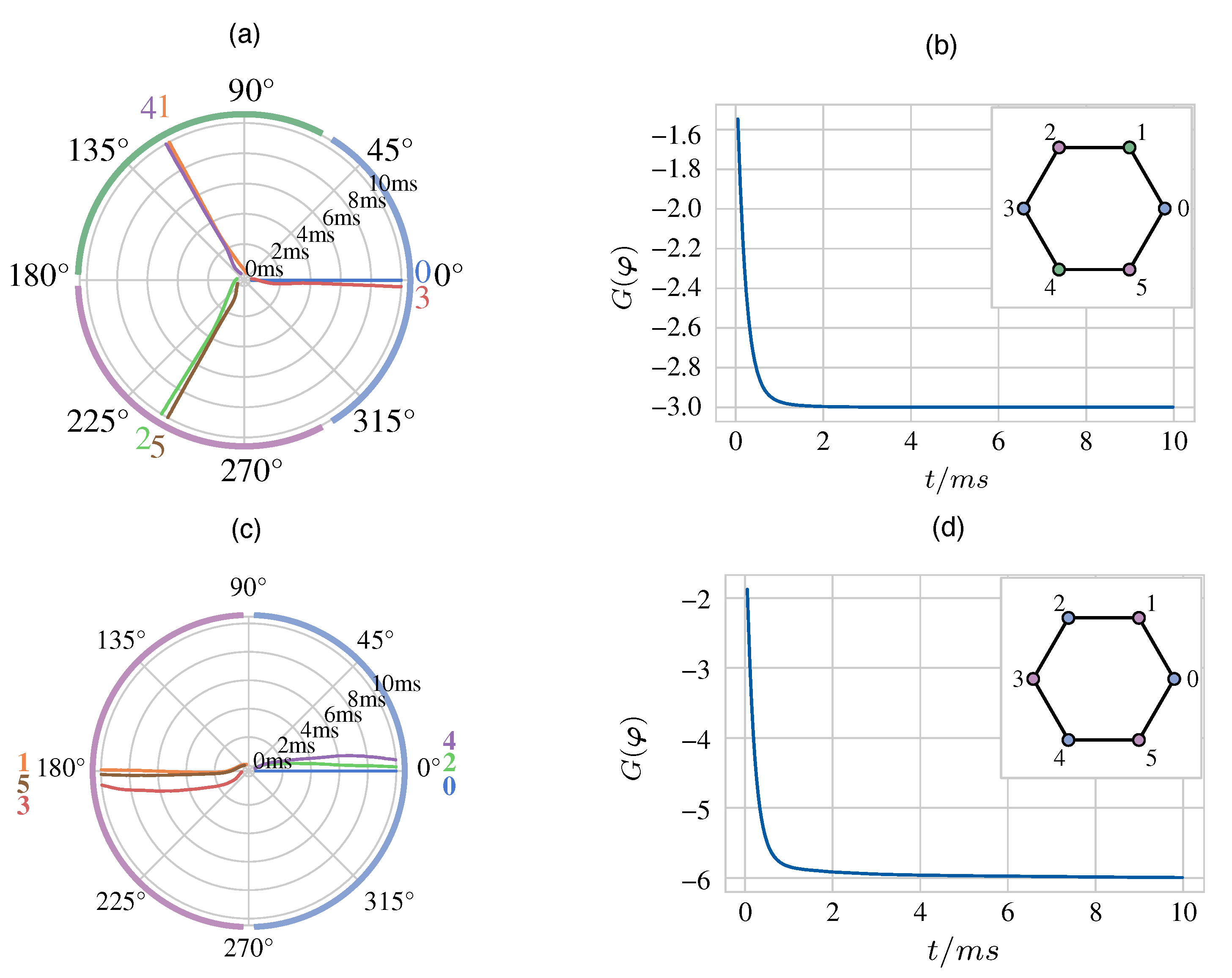
3.2. Compensation for an Imbalance in the Number of Couplings per Oscillator
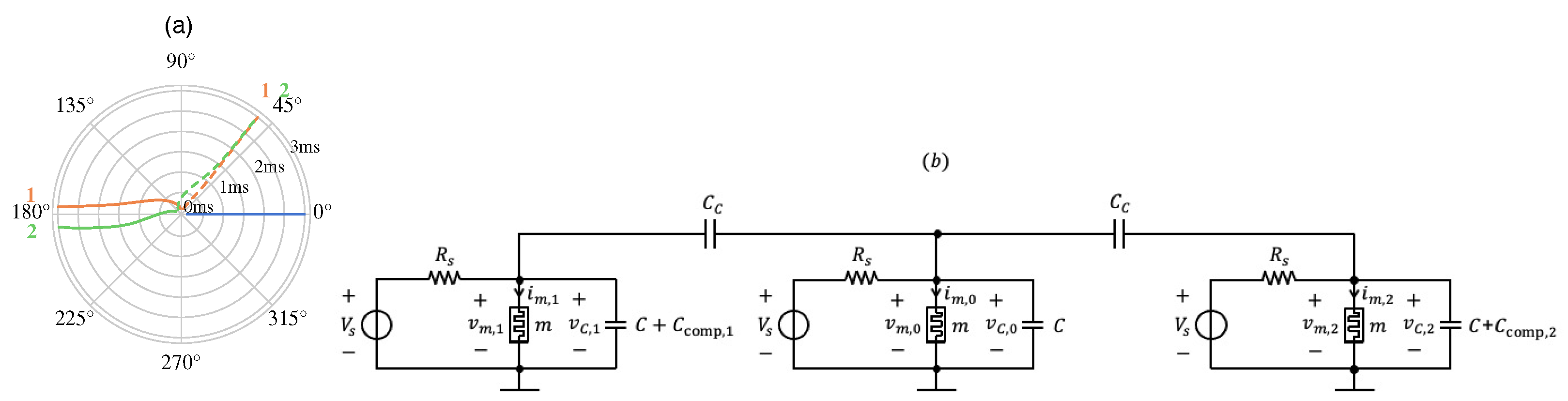
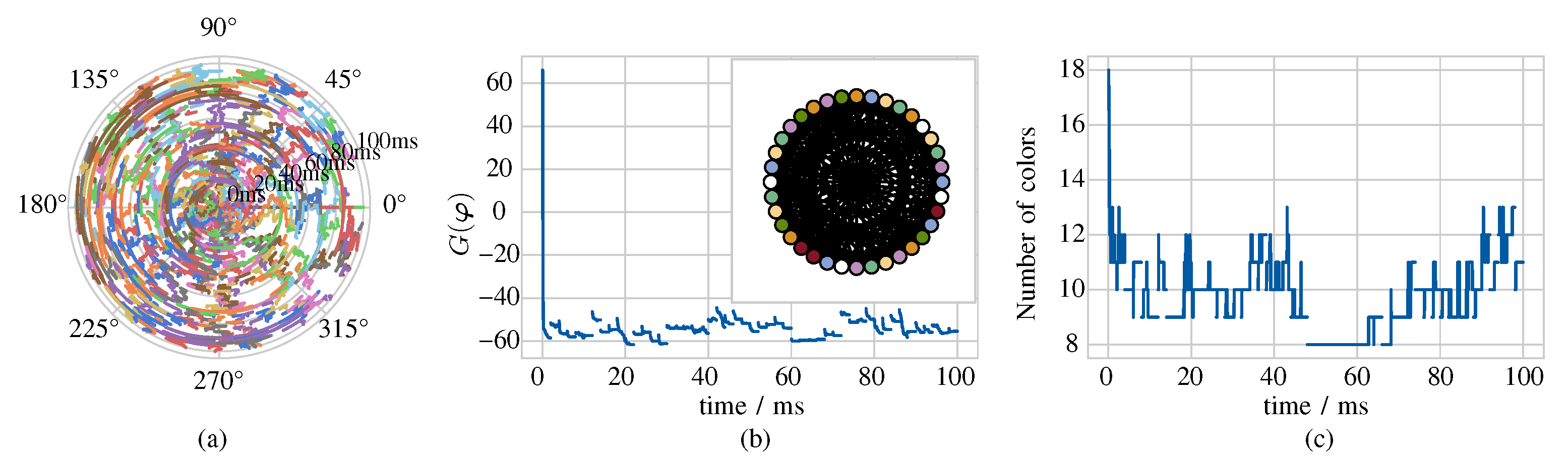
3.3. Compensation for the Memristor Device-to-Device Variability
4. A Rigorous Strategy for Coloring a Graph via the Network Phase Dynamics
5. Control Paradigms to Resolve Local Minima-Based Impasse Conditions
5.1. Crossover Strategy
- (1)
- For each value of k in the set , the vertex k is removed from the original N-node graph, and the iterative vertex coloring strategy is applied to the resulting graph of nodes, using a modified version of the vertex ranking, which is tabulated beforehand, after a simulation of the oscillatory network, under a generic sub-optimal initialisation setting, attains the steady state. Specifically, the label of the vertex k, taken out of the original graph, is removed from the original vertex ranking, resulting in a new table with entries. For each value of k, a matrix, denoted as , and obtained from the original adjacency matrix by setting to 0 all the elements at row k and at column k, may still be used to define the connectivity of the respective -node graph. Coloring the vertices of N distinct graphs, at least one of the N problems will be found to admit the best solution, allowing to categorise the nodes of the relative graph through the lowest number of color groups. The particular node k, which, extracted out of the original graph, allows the resulting network to identify the least number of colors according to our iterative vertex coloring procedure, may then be chosen as first vertex i to involve in the crossover20.
- (2)
- Assigning, one at a time, any integer from the set to k, the iterative vertex coloring strategy is then applied to a new vertex ranking, obtained from the original table by interchanging the positions of vertices i and k. Note that the original N-node graph, with connectivity defined by the adjacency matrix , should be considered in each of the applications of the iterative vertex coloring strategy, since nothing else, except for the correspondence between oscillators and vertices, is affected in a crossover operation21. Solving the resulting vertex coloring problems, the solution, assigning the least number of colors to the N nodes of the original graph, will be determined. It may happen that, on the basis of the proposed iterative procedure, for two or more values of k, the exchange between the positions of oscillators k and i in the original vertex ranking results in a common lowest number of color groups for the N nodes of the original graph. In this case, the choice of the second oscillator j to involve in the crossover falls for the particular candidate k, whose relative phase features the largest distance from the relative phase of oscillator i in the steady-state phase shift vector obtained through the simulation preceding the application of the two-step strategy.
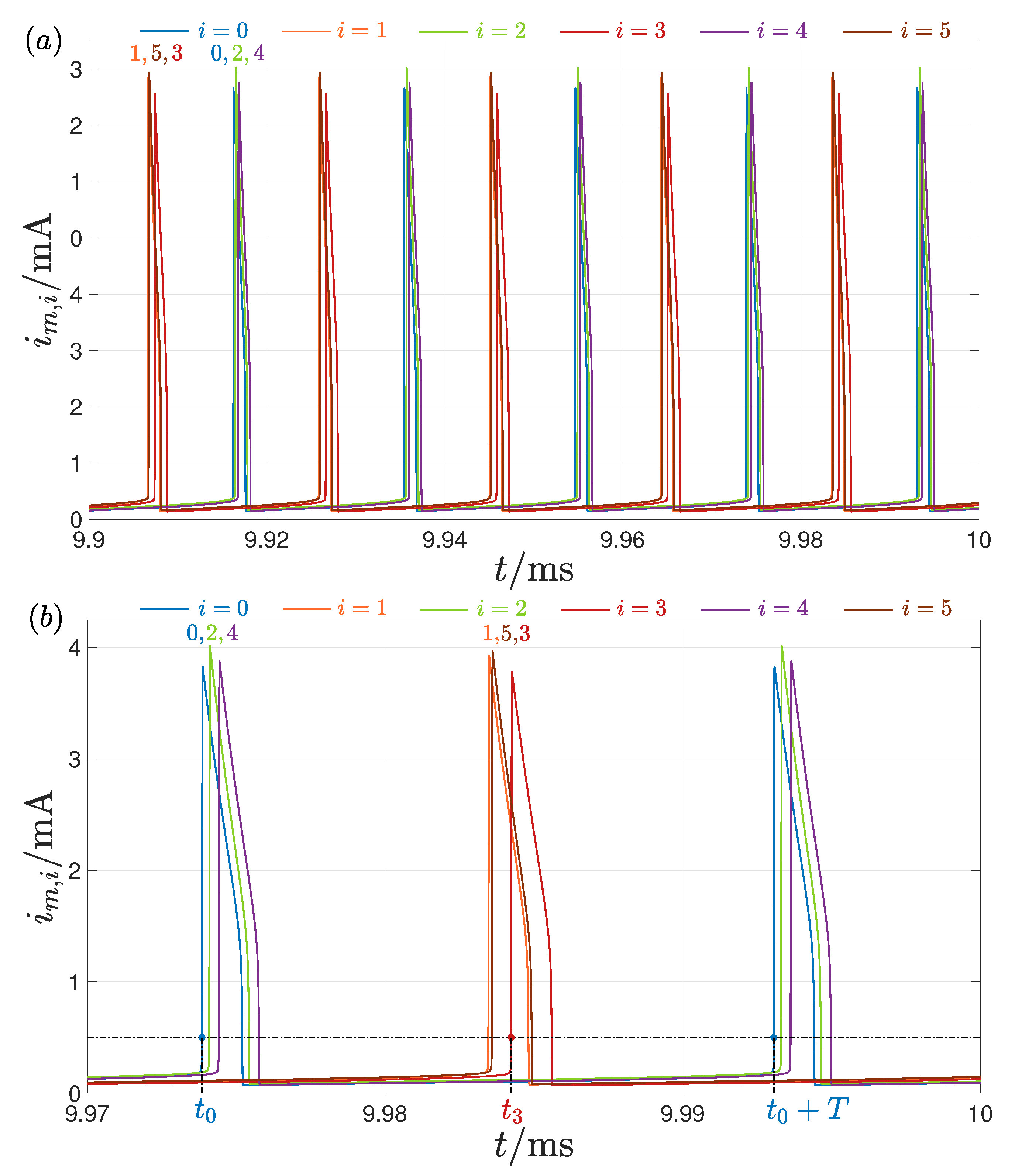
5.2. Pulse Destabilisation Strategy
- (1)
- The most suitable oscillator to target in the pulse destabilisation action is determined in the same way as was done for the selection of the cell to involve in the crossover process (see the first step in the procedure aimed to choose the right cell pair to involve in the coupling interchange strategy).
- (2)
- The second step is aimed to determine the appropriate shift to be added to the steady-state relative phase of oscillator i for pulling the network out of the local minimum state, facilitating its convergence to an oscillatory solution, which would ideally correspond to the least number of color groups for the N vertices of the associated graph. To accomplish this task, for each value of k within the set , with M a predefined positive integer, the offset is added to the phase shift of cell i in the steady-state relative phase shift vector recorded before the application of the pulse destabilisation process, and the iterative graph coloring procedure is applied to the resulting vertex ranking for the original graph. The choice for the most appropriate offset , within the specified set of k-dependent uniformly-spaced values, goes for the -candidate, which, according to our graph coloring strategy, allows the network to classify the nodes of the associated graph in the lowest number of color groups. If, for two or more k-values, the application of the iterative graph coloring procedure to the vertex ranking, resulting from the phase shift ordering, obtained by adding up the relevant offset to the phase shift of oscillator i in the steady-state relative phase shift vector , leads to the identification of the same lowest number of colors, the selection goes for the -candidate featuring the largest modulus. Finally, the pulse amplitude of the -long stimulus to be applied to oscillator i is obtained from Equation (33).
5.3. Discussion
6. Conclusions
Author Contributions
Funding
Data Availability Statement
Conflicts of Interest
References
- Chua, L.O. Memristor: The missing circuit element. IEEE Trans. Circuit Theory 1971, 18, 507–519. [Google Scholar] [CrossRef]
- Chua, L.O.; Kang, S. Memristive devices and systems. Proc. IEEE 1976, 64, 209–223. [Google Scholar] [CrossRef]
- Strukov, D.B.; Snider, G.S.; Stewart, D.R.; Williams, R.S. The missing memristor found. Nature 2008, 453, 80–83. [Google Scholar] [CrossRef] [PubMed]
- Prodomakis, T.; Toumazou, C.; Chua, L.O. Two Centuries of Memristors. Nat. Mater. 2012, 11, 478–481. [Google Scholar] [CrossRef] [PubMed]
- Chua, L.O. If It’s Pinched, It’s a Memristor. Semicond. Sci. Technol. 2014, 29, 104001. [Google Scholar] [CrossRef]
- Ielmini, D.; Waser, R. Resistive Switching: From Fundamentals of Nanoionic Redox Processes to Memristive Device Applications, 1st ed.; Wiley-VCH: Weinheim, Germany, 2016; ISBN -13: 978-3527334179. [Google Scholar]
- Mikolajick, T.; Salinga, M.; Kund, M.; Kever, T. Nonvolatile Memory Concepts Based on Resistive Switching in Inorganic Materials. Adv. Eng. Mater. 2009, 11, 235–240. [Google Scholar] [CrossRef]
- Indiveri, G.; Linares-Barranco, B.; Legenstein, R.; Deligeorgis, G.; Prodromakis, T. Integration of nanoscale memristor synapses in neuromorphic computing architectures. Nanotechnology 2013, 24, 384010. [Google Scholar] [CrossRef] [Green Version]
- Pickett, M.D.; Medeiros-Ribeiro, G.; Williams, R.S. A scalable neuristor built with Mott memristors. Nat. Mater. 2013, 12, 114–117. [Google Scholar] [CrossRef]
- Yi, W.; Tsang, K.K.; Lam, S.K.; Bai, X.; Crowell, J.A.; Flores, E.A. Biological plausibility and stochasticity in scalable VO2 active memristor neurons. Nat. Commun. 2018, 9, 1–10. [Google Scholar] [CrossRef]
- Kang, S.M.; Choi, D.; Eshraghian, J.K.; Zhou, P.; Kim, J.; Kong, B.S.; Zhu, X.; Demirkol, A.S.; Ascoli, A.; Tetzlaff, R.; Lu, W.D.; Chua, L.O. How to Build a Memristive Integrate-and-Fire Model for Spiking Neuronal Signal Generation. IEEE Trans. Circuits Syst. I Regul. Pap. 2021, 68, 4837–4850. [Google Scholar] [CrossRef]
- Tetzlaff, R.; Ascoli, A.; Messaris, I.; Chua, L.O. Theoretical Foundations of Memristor Cellular Nonlinear Networks: Memcomputing with Bistable-like Memristors. IEEE Trans. Circuits Syst. I Regul. Pap. 2020, 67, 502–515. [Google Scholar] [CrossRef]
- Ascoli, A.; Messaris, I.; Tetzlaff, R.; Chua, L.O. Theoretical Foundations of Memristor Cellular Nonlinear Networks: Stability Analysis with Dynamic Memristors. IEEE Trans. Circuits Syst. I Regul. Pap. 2020, 67, 1389–1401. [Google Scholar] [CrossRef]
- Ascoli, A.; Tetzlaff, R.; Kang, S.M.; Chua, L.O. Theoretical Foundations of Memristor Cellular Nonlinear Networks: A DRM2-based Method to Design Memcomputers with Dynamic Memristors. IEEE Trans. Circuits Syst. I Regul. Pap. 2020, 67, 2753–2766. [Google Scholar] [CrossRef]
- Chua, L.O. (Ed.) CNN: A Paradigm for Complexity; World Scientific Series on Nonlinear Science: Singapore, 1998; ISBN 978-9810234836. [Google Scholar]
- Xia, Q.; Yang, J.J. Memristive crossbar arrays for brain-inspired computing. Nat. Mater. 2019, 18, 309–323. [Google Scholar] [CrossRef] [PubMed]
- Ventra, M.D.; Traversa, F.L. Perspective: Memcomputing: Leveraging memory and physics to compute efficiently. J. Appl. Phys. 2018, 123, 180901. [Google Scholar] [CrossRef] [Green Version]
- Talati, N.; Gupta, S.; Mane, P.; Kvatinsky, S. Logic Design within Memristive Memories Using Memristor Aided loGIC (MAGIC). IEEE Trans. Nanotechnol. 2016, 15, 635–650. [Google Scholar] [CrossRef]
- Ali, A.H.; Hur, R.B.; Wald, N.; Ronen, R.; Kvatinsky, S. Not in Name Alone: A Memristive Memory Processing Unit for Real In-Memory Processing. IEEE Micro 2018, 38, 13–21. [Google Scholar]
- Ielmini, D.; Wong, H.-S.P. In-memory computing with resistive switching devices. Nat. Electron. 2018, 1, 333–343. [Google Scholar] [CrossRef]
- Tzouvadaki, I.; Jolly, P.; Lu, X.; Ingebrandt, S.; de Micheli, G.; Estrela, P.; Carrara, S. Label-Free Ultrasensitive Memristive Aptasensor. Nanoletters 2016, 16, 4472–4476. [Google Scholar] [CrossRef] [Green Version]
- Ibarlucea, B.; Akbar, T.F.; Kim, K.; Rim, T.; Baek, C.-K.; Ascoli, A.; Tetzlaff, R.; Baraban, L.; Cuniberti, G. Ultrasensitive Detection of Ebola Matrix Protein in a memristor mode. NanoResearch 2018, 11, 1057–1068. [Google Scholar] [CrossRef]
- Wang, Z.; Joshi, S.; Savel’ev, S.; Song, W.; Midya, R.; Li, Y.; Rao, M.; Yan, P.; Asapu, S.; Zhuo, Y.; et al. Fully memristive neural networks for pattern classification with unsupervised learning. Nat. Electron. 2018, 1, 137–145. [Google Scholar] [CrossRef]
- Sebastian, A.; Tuma, T.; Papandreou, N.; Gallo, M.L.; Kull, L.; Parnell, T.; Eleftheriou, E. Temporal correlation detection using computational phase-change memory. Nat. Commun. 2017, 8, 1115. [Google Scholar] [CrossRef] [PubMed]
- Sheng, X.; Graves, C.E.; Kumar, S.; Li, X.; Buchanan, B.; Zheng, L.; Lam, S.; Li, C.; Strachan, J.P. Low-Conductance and Multilevel CMOS-Integrated Nanoscale Oxide Memristors. Adv. Electron. Mater. 2019, 5, 1800876. [Google Scholar] [CrossRef]
- Chua, L.O. Local activity is the origin of complexity. Int. J. Bifurc. Chaos 2005, 15, 3435–3456. [Google Scholar] [CrossRef] [Green Version]
- Pickett, M.D.; Williams, R.S. Sub-100 fJ and sub-nanosecond thermally driven threshold switching in niobium oxide crosspoint nanodevices. Nanotechnology 2012, 23, 215202. [Google Scholar] [CrossRef]
- Ascoli, A.; Slesazeck, S.; Ma¨hne, H.; Tetzlaff, R.; Mikolajick, T. Nonlinear dynamics of a locally-active memristor. IEEE Trans. Circuits Syst. I (TCAS–I) Regul. Pap. 2015, 62, 1165–1174. [Google Scholar] [CrossRef]
- Cai, F.; Kumar, S.; Vaerenbergh, T.V.; Sheng, X.; Liu, R.; Li, C.; Liu, Z.; Foltin, M.; Yu, S.; Xia, Q.; Yang, J.J.; Beausoleil, R.; Lu, W.D.; Strachan, J.P. Power-efficient combinatorial optimization using intrinsic noise in memristor Hopfield neural networks. Nat. Electron. 2020, 3, 409–418. [Google Scholar] [CrossRef]
- Weiher, M.; Herzig, M.; Tetzlaff, R.; Ascoli, A.; Mikolajick, T.; Slesazeck, S. Pattern formation with local active S-type NbOx memristors. IEEE Trans. Circuits Syst. I Regul. Pap. 2019, 66, 2627–2638. [Google Scholar] [CrossRef]
- Weiher, M.; Herzig, M.; Tetzlaff, R.; Ascoli, A.; Slesazeck, S.; Mikolajick, T. Improved Vertex Coloring With NbOx Memristor-Based Oscillatory Networks. IEEE Trans. Circuits Syst. I 2021, 68, 2082–2095. [Google Scholar] [CrossRef]
- Va´zquez, A.R.; Ferna´ndez-Berni, J.; Len˜ero-Bardallo, J.A.; Vornicu, I.; Carmona-Gala´n, R. CMOS Vision Sensors: Embedding Computer Vision at Imaging Front-Ends. IEEE Circuits Syst. Mag. 2018, 18, 90–107. [Google Scholar] [CrossRef]
- Ascoli, A.; Weiher, M.; Herzig, M.; Tetzlaff, R.; Slesazeck, S.; Mikolajick, T. Control Strategies to Optimize Graph Coloring via M-CNNs with Locally-Active NbOx Memristors. In Proceedings of the International Conference on Modern Circuits and Systems Technologies (MOCAST) on Electronics and Communications, Thessaloniki, Greece, 5–7 July 2021. [Google Scholar]
- Slesazeck, S.; Ma¨hne, H.; Wylezich, H.; Wachowiak, A.; Radhakrishnan, J.; Ascoli, A.; Tetzlaff, R.; Mikolajick, T. Physical model of threshold switching in NbO2 based memristors. J. R. Soc. Chem. 2015, 5, 102318–102322. [Google Scholar] [CrossRef]
- Slesazeck, S.; Herzig, M.; Mikolajick, T.; Ascoli, A.; Weiher, M.; Tetzlaff, R. Analysis of Vth variability in NbOx-based threshold switches. In Proceedings of the IEEE Nonvolatile Memory Technology Symposium (NVMTS), Pittsburgh, PA, USA, 17–19 October 2016; Carnegie Mellon University: Pittsburgh, PA, USA, 2016. [Google Scholar] [CrossRef]
- Gibson, G.A.; Musunuru, S.; Zhang, J.; Vandenberghe, K.; Lee, J.; Hsieh, C.-C.; Jackson, W.; Jeon, Y.; Henze, D.; Li, Z.; Williams, R.S. An accurate locally active memristor model for S-type negative differential resistance in NbOx. Appl. Phys. Lett. 2016, 108, 023505. [Google Scholar] [CrossRef] [Green Version]
- Herzig, M.; Weiher, M.; Ascoli, A.; Tetzlaff, R.; Mikolajick, T.; Slesazeck, S. Multiple slopes in the negative differential resistance region of NbOx-based threshold switches. J. Phys. D Appl. Phys. 2019, 52, 325104. [Google Scholar] [CrossRef]
- Herzig, M.; Weiher, M.; Ascoli, A.; Tetzlaff, R.; Mikolajick, T.; Slesazeck, S. Improvement of NbOx-based threshold switching devices by implementing multilayer stacks. Semicond. Sci. Technol. 2019, 34, 075005. [Google Scholar] [CrossRef]
- Pickett, M.D.; Strukov, D.B.; Borghetti, J.L.; Yang, J.J.; Snider, G.S.; Stewart, D.R.; Williams, R.S. Switching dynamics in titanium dioxide memristive devices. J. Appl. Phys. 2009, 106, 074508. [Google Scholar] [CrossRef]
- Chua, L.O. Five Non-Volatile Memristor Enigmas Solved. Appl. Phys. A 2018, 124, 563. [Google Scholar] [CrossRef]
- Wu, C.W. Graph Coloring via Synchronization of Coupled Oscillators. IEEE Trans. Circuits Syst. I Fundam. Theory Appl. 1998, 45, 974–978. [Google Scholar]
- Parihar, A.; Shukla, N.; Jerry, M.; Datta, S.; Raychowdhury, A. Vertex coloring of graphs via phase dynamics of coupled oscillatory networks. Sci. Rep. 2017, 7, 1–11. [Google Scholar] [CrossRef] [Green Version]
- Ascoli, A.; Demirkol, A.S.; Tetzlaff, R.; Slesazeck, S.; Mikolajick, T.; Chua, L.O. On Local Activity and Edge of Chaos in a NaMLab Memristor. Front. Neurosci. 2021, 15. [Google Scholar] [CrossRef]
- Ascoli, A.; Demirkol, A.S.; Tetzlaff, R.; Chua, L.O. Edge of Chaos Theory Resolves Smale Paradox. IEEE Trans. Circuits Syst. I Reg. Pap. 2022, 69, 252–1265. [Google Scholar] [CrossRef]
- Mitchell, M. An Introduction to Genetic Algorithms; MIT Press: Cambridge, MA, USA, 1998; ISBN 978-0262631853. [Google Scholar]
- Chibante, R. Simulated Annealing: Theory with Applications; Sciyo: Rijeka, Croatia, 2010; ISBN 978-953-307-134-3. [Google Scholar]
- Ascoli, A.; Baumann, D.; Tetzlaff, R.; Chua, L.O.; Hild, M. Memristor-enhanced humanoid robot control system–Part I: Theory behind the novel memcomputing paradigm. Int. J. Circuit Theory Appl. IJCTA 2018, 46, 155–183. [Google Scholar] [CrossRef]
- Baumann, D.; Ascoli, A.; Tetzlaff, R.; Chua, L.O.; Hild, M. Memristor-enhanced humanoid robot control system–Part II: Circuit theoretic model and performance analysis. Int. J. Circuit Theory Appl. IJCTA 2018, 46, 184–220. [Google Scholar] [CrossRef]
- Sharma, A.A.; Bain, J.A.; Weldon, J.A. Phase coupling and control of oxide-based oscillators for neuromorphic computing. IEEE J. Explor. Solid-State Comput. Devices Circuits 2015, 1, 58–66. [Google Scholar] [CrossRef]
- Graph Coloring Instances. Available online: https://mat.tepper.cmu.edu/COLOR/instances.html (accessed on 25 March 2022).
- Johnson, D.S.; Trick, M.A. Cliques, Coloring, and Satisfiability: Second DIMACS Implementation Challenge; Based upon the Proceedings of the DIMACS Workshop, 11–13 October 1993; Series in Discrete Mathematics and Theoretical Computer Science; American Mathematical Society: Providence, RI, USA, 1996; Volume 26. [Google Scholar]
- Brélaz, D. New Methods to Color the Vertices of a Graph. Commun. Assoc. Comput. Mach. ACM 1979, 22, 251–256. [Google Scholar] [CrossRef]
- Pickett, M.D.; Williams, R.S. Phase transitions enable computational universality in neuristor-based cellular automata. Nanotechnology 2013, 24, 384002. [Google Scholar] [CrossRef] [Green Version]
- Messaris, I.; Brown, T.D.; Demirkol, A.S.; Ascoli, A.; Chawa, M.M.A.; Williams, R.S.; Tetzlaff, R.; Chua, L.O. NbO2-Mott Memristor: A Circuit-Theoretic Investigation. IEEE Trans. Circuits Syst. I Regul. Pap. 2021, 68, 4979–4992. [Google Scholar] [CrossRef]
- Liu, X.; Zhang, P.; Nath, S.K.; Li, S.; Nandi, S.K.; Elliman, R.G. Understanding composite negative differential resistance in niobium oxide memristors. J. Phys. D Appl. Phys. 2022, 55, 105106. [Google Scholar] [CrossRef]
- Callarotti, R.C.; Schmidt, P.E. Theoretical and experimental study of the operation of ovonic switches in the relaxation oscillation mode. I. The charging characteristic during the off state. J. Appl. Phys. 1984, 55, 3144. [Google Scholar] [CrossRef]
- Callarotti, R.C.; Schmidt, P.E. Theoretical and experimental study of the operation of ovonic switches in the relaxation oscillation mode. II. The discharging characteristics and the equivalent circuits. J. Appl. Phys. 1984, 55, 3148. [Google Scholar] [CrossRef]
- Kim, S.J.; Cho, S.W.; Lee, H.; Lee, J.; Seong, T.Y.; Kim, I.; Park, J.-K.; Kwak, J.Y.; Kim, J.; Park, J.; et al. Frequency-tunable nano-oscillator based on Ovonic Threshold Switch (OTS).
- Demirkol, A.S.; Ascoli, A.; Messaris, I.; Tetzlaff, R. Pattern formation dynamics in an MCNN structure with a numerically stable VO2 memristor model. Jpn. J. Appl. Phys. under review.
| 1 | The time it takes for a von Neumann computing machine to find the optimal solution to a NP-hard problem, which involves n elements, scales exponentially with n. |
| 2 | |
| 3 | Importantly, depending upon the graph under focus, the proposed Memristor CNN (M-CNN) may feature either local or non-local capacitive couplings. The solution of the vertex coloring problem through the proposed M-CNNs depends upon the phase differences among the oscillations developing in the constitutive units of the array at steady state. In order to highlight the steady-state oscillatory behaviours of the cells during operation, the bio-inspired arrays are also referred to as Memristor Oscillatory Networks (MONs) in the remainder of the manuscript. |
| 4 | |
| 5 | It is instructive to observe that there exist memristor physical realisations, whose models feature an even more general input- and state- dependent Ohm law than what is admissible for extended memristors. For these two-terminal devices, including the TiO memristor from HP Labs [39], the mathematical description includes an implicit Ohm law of the form , with x, , and denoting the device state, voltage, and current, respectively. |
| 6 | The mathematical description of the nonlinear resistor, formulated in Equation (3), is in fact equivalent to the model of a NbO memristor, as originally presented in [34,35], which reveals the correspondence of the real parameters , and to physical properties of the nanostructure, in the limit when changes occurring in the device state, defined as its body temperature, are negligible. |
| 7 | The nominal parameter setting is obtained from Table 1 for . As will be shown later, simulating the memristor model under a quasi-DC voltage stimulus and with the variability parameter stepped across its existence domain, the locus observed for appears in the center of the distribution of characteristics emerging in the voltage-current plane. |
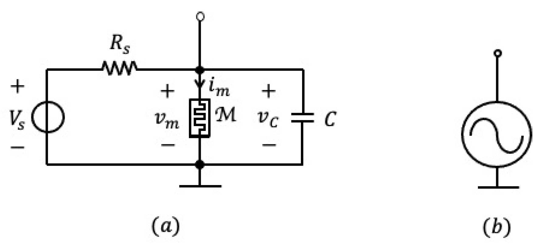
| 8 | The voltage across (current through) the memristor in the cell i is indicated via (). |
| 9 | The units of the steady-state relative phase of oscillator i, computed via , are radiants. In order to express in degrees, its formula needs to be scaled by the factor (). |
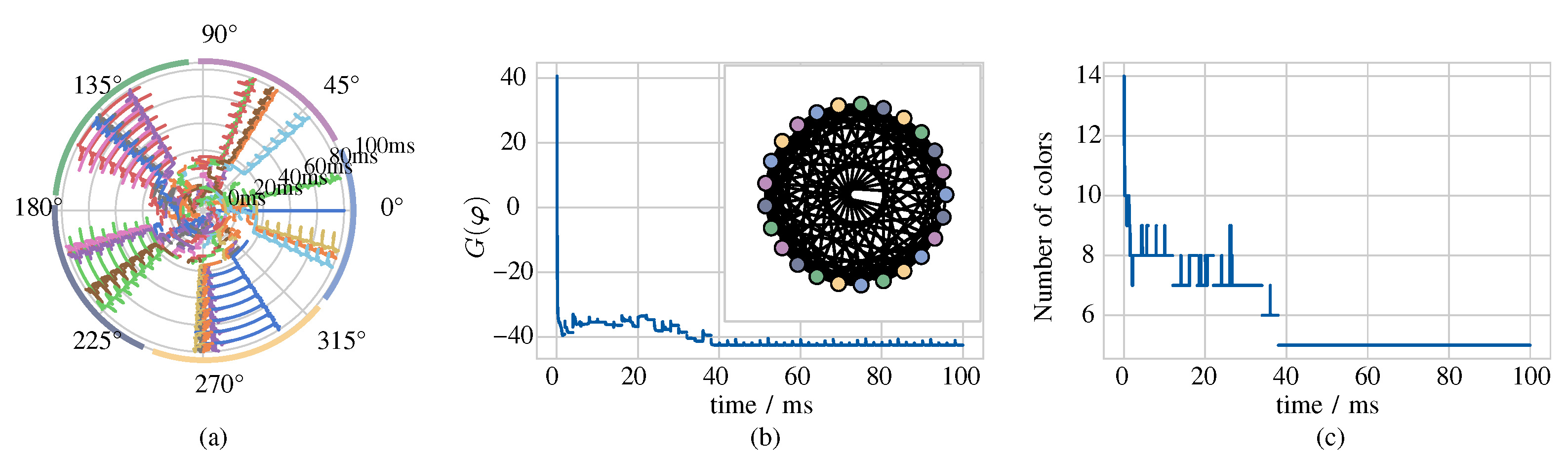
| 10 | A new graphical tool—which we call phase diagram—is introduced in this research study [31] for visualising the phase dynamics of the network. Referring, for example, to the phase diagram of Figure 6(a), a specific trace visualises the time evolution of the phase of oscillator j relative to oscillator 0 (). Reading the time flow along the radial direction, the angle between the segment, joining the origin to the point, where the trace is found to lie at time t, and the blue horizontal line, denoting the -valued reference level, represents the phase shift of oscillator j with respect to oscillator 0 at time t. |
| 11 | The natural frequency of an oscillator is the inverse of the period of the oscillations developing across its circuitry. |
| 12 | In order to reprogram appropriately the operating point of the memristor in the cell of the 3-oscillator network under focus, the cell j itself is capacitively coupled only to the reference cell 0, and, as described earlier, is tuned until anti-phase synchronisation emerges in the resulting two-cell network. This procedure is carried out separately for oscillators 1 and 2. |
| 13 | It is important to pinpoint that, while the choice of a reference cell for the preliminary compensation of the memristor device-to-device variability should fall for a specific oscillator, as specified here, no rule dictates the selection of a reference cell for the later computation of the relative phase pattern of the array, as discussed in Section 4. |
| 14 | It is important to observe that, while taking the proposed device-to-device compensation measure, care need to be taken so as to keep the natural oscillation frequency of each oscillator within a close range. In fact, a wide spread in this parameter, inevitably differing across the cellular medium, due to the tuning procedure, would jeopardize the convergence of the bio-inspired computing engine to some steady state. |
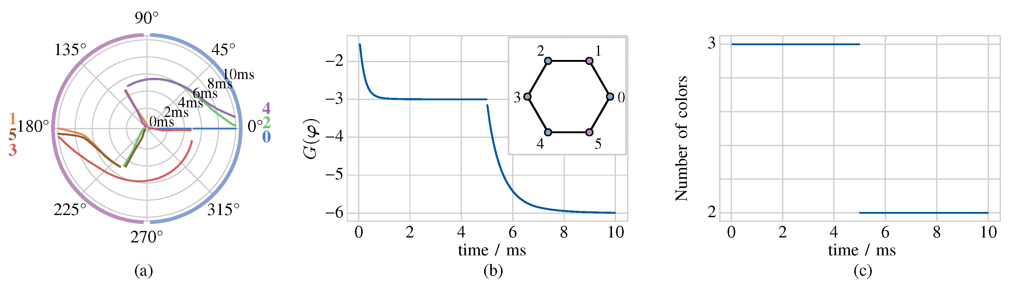
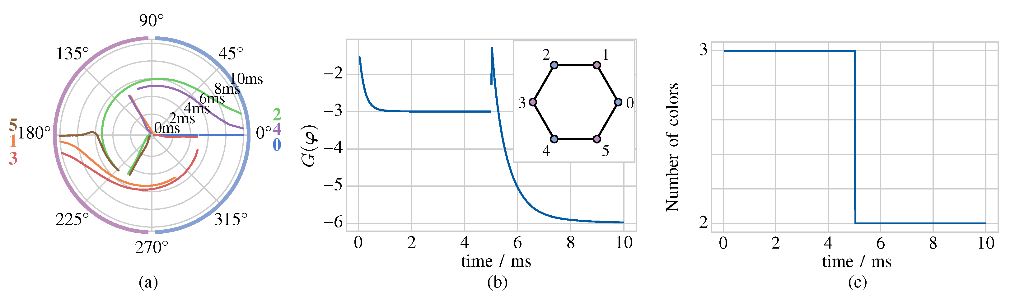
| 15 | The proposed strategy will determine the minimum possible number of color groups, which, under a given initialisation setting, the network is able to identify as it classifies the nodes of the associated graph. Importantly, as will be clarified later, this minimum number does not necessarily coincide with the chromatic number of graph, since the network may converge to a correct but suboptimal solution. Methods allowing the memristive array to overcome a suboptimal solution so as to approach the optimal one will be presented shortly. |
| 16 | If an (no) edge connects vertices i and j, then . Note that . |
| 17 | Since, here, oscillator i is associated to vertex i for each , the oscillator sequence, corresponding to the phase shift ordering, may be indifferently referred to as oscillator ranking or vertex ranking. As will be clarified later on, this is not always the case, when perturbation actions are performed on the network to enhance its performance. |
| 18 | in this work the estimation of the common period T of the oscillations developing in a N-cell network, and the associated group ordering of the phase shifts of the cells 1, …, relative to the null phase of the reference cell 0 are carried out every cycle throughout the duration of any simulation. |
| 19 | The application of a crossover to pairs of oscillators implies the necessity to endow the network with reprogrammable connections, e.g. via transistor-based switches, which, however, would add on to the integrated circuit (IC) overhead in a future hardware implementation of the network. |
| 20 | In fact, it is highly probable that this node mostly prevents the optimisation measure of Equation (16) from attaining the global minimum, which would provide as solution to the vertex coloring task the chromatic number of the original N-node graph, as desired. In case, for each of two or more values of k, the application of our vertex coloring strategy to the respective -node graph, obtained by removing the vertex k from the original graph, results in a common lowest number of colors, any of these node i candidates may be finally considered for the crossover |
| 21 | The interchange between nodes i and k operated on the original vertex ranking is due to the fact that the application of a crossover between the corresponding oscillators in the network is equivalent to exchanging their associations to the respective pair of vertices in the original graph. The relative phases, inherent to the oscillators, maintain the same ordering, as established originally. As a result, the oscillator ranking remains unaltered, but the mapping from oscillator ranking to vertex ranking is subject to the earlier mentioned node interchange. |
| 22 | In this work was set to twice the common graph-dependent period T of the oscillatory waveforms of the capacitor voltages and of the memristor currents in the network before the application of the pulse destabilisation paradigm. |
| 23 | We acknowledge, however, that the most suitable formula, expressing the relationship between the amplitude of a destabilising pulse of fixed width and the resulting sudden shift in the phase of the perturbed oscillator, may depend upon network properties and parameters. A deeper study, aimed to optimise the shape of the destabilisation stimulus, will be carried out in the future. |
| 24 | In order to present a fair comparison between the beneficial effects of the crossover and pulse destabilisation control paradigms, we ensured that the simulations in Figure 11 and Figure 12 provided identical results for ms by choosing the same initialisation setting, and assigning a common random set of -values to the memristors. |
| 25 | In some cases, after overcoming the impasse situation, the dynamical system could approach a new oscillatory solution associated to another local minimum of . |
| 26 | The time separation between consecutive applications of the crossover or pulse destabilisation strategy is set to ms in the simulations discussed in this section. Furthermore, in this work the estimation of the common period T of the oscillations appearing in a N-cell network, and the associated group ordering of the phase shifts of the cells 1, …, relative to the null phase of the reference cell 0 are carried out every cycle throughout the duration of any simulation. Moreover, in the first (latter) control strategy, the application of a pulse to the same oscillator (a crossover involving either oscillator from the same pair) is not allowed until at least 5 iterations of the control strategy have elapsed first. As a result, each pulse destabilisation (crossover) manoeuvre targets a different oscillator (involves a different pair of oscillators). |


| J · K | W · K | K | K | |
| 293 | ||||
| K· V | K | K· V | ||
| 1000 |
| V | F | F | |
|---|---|---|---|
| 5525 |
| Minimum Number of Color Groups for the Classification of the Vertices of the Associated Group | |||||||
|---|---|---|---|---|---|---|---|
| graph | vertices | n | Brélaz algorithm | [42] | iterative strategy | iterative strategy and crossover control | iterative strategy and pulse destabilisation control |
| mycie13 | 11 | 4 | 4 | 4 | 4 | 4 | 4 |
| mycie14 | 20 | 5 | 5 | 5 | 5 | 5 | 5 |
| mycie15 | 47 | 6 | 6 | 6 | 7 | 6 | 6 |
| queen5_5 | 25 | 5 | 7 | 6 | 7 | 5 | 5 |
| queen6_6 | 36 | 7 | 10 | 12 | 11 | 8 | 8 |
| queen7_7 | 49 | 7 | 12 | 12 | 14 | 10 | 10 |
| queen8_8 | 64 | 9 | 15 | 14 | 15 | 13 | 13 |
Publisher’s Note: MDPI stays neutral with regard to jurisdictional claims in published maps and institutional affiliations. |
© 2022 by the authors. Licensee MDPI, Basel, Switzerland. This article is an open access article distributed under the terms and conditions of the Creative Commons Attribution (CC BY) license (https://creativecommons.org/licenses/by/4.0/).
Share and Cite
Ascoli, A.; Weiher, M.; Herzig, M.; Slesazeck, S.; Mikolajick, T.; Tetzlaff, R. Graph Coloring via Locally-Active Memristor Oscillatory Networks. J. Low Power Electron. Appl. 2022, 12, 22. https://doi.org/10.3390/jlpea12020022
Ascoli A, Weiher M, Herzig M, Slesazeck S, Mikolajick T, Tetzlaff R. Graph Coloring via Locally-Active Memristor Oscillatory Networks. Journal of Low Power Electronics and Applications. 2022; 12(2):22. https://doi.org/10.3390/jlpea12020022
Chicago/Turabian StyleAscoli, Alon, Martin Weiher, Melanie Herzig, Stefan Slesazeck, Thomas Mikolajick, and Ronald Tetzlaff. 2022. "Graph Coloring via Locally-Active Memristor Oscillatory Networks" Journal of Low Power Electronics and Applications 12, no. 2: 22. https://doi.org/10.3390/jlpea12020022
APA StyleAscoli, A., Weiher, M., Herzig, M., Slesazeck, S., Mikolajick, T., & Tetzlaff, R. (2022). Graph Coloring via Locally-Active Memristor Oscillatory Networks. Journal of Low Power Electronics and Applications, 12(2), 22. https://doi.org/10.3390/jlpea12020022