Article

The Effect of Zirconium Doping on Solution-Processed Indium Oxide Thin Films Measured by a Novel Nondestructive Testing Method (Microwave Photoconductivity Decay)

1
State Key Laboratory of Luminescent Materials and Devices, Institute of Polymer Optoelectronic Materials and Devices, South China University of Technology, Guangzhou 510640, China
2
State Key Laboratory of Mechanics and Control of Mechanical Structures, Nanjing University of Aeronautics and Astronautics, Nanjing 210016, China
3
School of Materials Science and Engineering, Beihang University, Beijing 100191, China
*
Authors to whom correspondence should be addressed.
Coatings 2019, 9(7), 426; https://doi.org/10.3390/coatings9070426
Submission received: 4 June 2019 / Revised: 3 July 2019 / Accepted: 4 July 2019 / Published: 5 July 2019
(This article belongs to the Special Issue Thin Films for Electronic Applications)

Abstract

:
Solution-processed indium oxide is an ideal transparent semiconductor material with wide band gap. Zirconium is an element characterized by a strong binding ability to oxygen which can inhibit the formation of oxygen vacancies and reduce the surface defect state. In this paper, zirconium doped indium oxide (InxZryO) thin films were prepared by the solution method, with indium oxide being doped with zirconium in order to tune the relative number of oxygen vacancies. The influence of the Zr doping concentration and the post-annealed temperature on the properties of the InxZryO thin films was investigated. The results show that the doping process improves the crystallinity and relative density of the obtained films. A novel nondestructive method named microwave photoconductivity decay (μ-PCD) was used to evaluate the quality of InxZryO thin films by simply measuring their response under laser irradiation. The relative number of oxygen vacancies and the minority carrier concentration achieved minimum values at 10 at.% Zr doping concentration. Furthermore, InxZryO thin films with optimal properties from an electrical point of view were obtained at 10 at.% Zr doping concentration, annealed at 400 °C. Characterized by an average transmittance above 90% in the visible range, the obtained InxZryO thin films can be used as active layer materials in the fabrication of high-performance thin film transistor (TFT) devices.

1. Introduction

Nowadays, active matrix liquid crystal displays (AMLCD) and active matrix organic light-emitting diodes (AMOLED) have occupied the mainstream position in the display field [1,2,3,4]. As the important component of flat-panel displays (FPDs), thin film transistors (TFTs) have attracted widespread attention. Metal oxide thin film transistors (MOS-TFTs) have been widely studied due to their advantages of high mobility, high optical transmittance, low process temperature, and low processing cost [5,6,7,8,9].
The MOS-TFT device prepared by Magnetron sputtering presents excellent electrical characteristics, but it has shortcomings such as relatively complex fabrication process, high cost and RF radiation damage. Solution-processed MOS films exhibit many advantages such as low cost, and the prepared films have excellent uniformity and high component purity [1,10,11,12,13,14]. The solution-processing method mainly includes dip coating, spraying, spin coating, printing, and so on. Spin coating is one of the most used methods. It has the advantages of uniform film making, low cost, simplicity, and high throughput. However, solution-processed films still suffer from high porosity and poor quality, which have a great influence on the properties of thin films [13,14,15,16].
Indium oxide (In2O3) films have high electron mobility, high carrier density, and excellent optical transmittance compared with other oxide semiconductors [17,18], making them an ideal material for transparent thin film transistors [19]. In order to obtain high-quality In2O3 films, other elements are added, such as InSnO (ISO) [20,21,22], InZnSnO (IZTO) [23,24,25,26], InGaZnO (IGZO) [27,28,29,30], etc. The Zr element has a strong binding capacity to oxygen (Zr–O: 776 KJ/mol), higher than that of the In element to oxygen (In–O: 348 KJ/mol), which can inhibit the formation of oxygen vacancies. Moreover, the radius of Zr4+ (0.72 Å) is close to the radius of In3+ (0.79 Å), so the addition will form a stable lattice structure [31,32].
Microwave photoconductivity decay (μ-PCD) is a noncontact and nondestructive technology with low cost and short time [33,34,35]. Information regarding the defect state density can be obtained by the microwave reflectivity of the photo-carrier trapping and recombination, this being an important parameter for the evaluation of the quality of the semiconductor thin films.
In this research, zirconium doped indium oxide (InxZryO) films were prepared on UV-treated substrates. Atomic force microscopy (AFM), thermogravimetry-differential scanning calorimetry (TG-DSC), X-ray reflectivity (XRR), X-ray diffraction (XRD), X-ray photoelectron spectroscopy (XPS), and microwave photoconductivity decay (μ-PCD) were used to evaluate the physical and chemical properties of InxZryO films. The influence of the Zr doping concentration and the post-annealed temperature on the properties of InxZryO films was discussed.

2. Materials and Methods

The precursor solutions were prepared by dissolving indium nitrate [In(NO3)3] and zirconium nitrate pentahydrate [Zr(NO3)4·5H2O] at different ratios (Zr:In = 0 at.%, 5 at.%, 10 at.%, 15 at.%) in 2-methoxyethanol. These solutions were stirred vigorously for 24 h and then were aged for 48 h under ambient conditions. The surface tension and contact angle of these solutions were measured by an Attension Theta Lite (Biolin Scientific, Gothenburg, Sweden, TL200). Thermogravimetric differential scanning calorimetry (TG-DSC) was used to measure the thermal behavior of precursor solutions with a heating rate of 10 °C/min (from room temperature to 600 °C).
The substrates were cleaned by UV/ozone at 25 °C for 2 min. The InxZryO thin films were fabricated by spin coating on the glass substrate at 5000 rpm for 40 s and then post-annealed at varying temperatures (250, 300, 350, and 400 °C) for 1 hour under air. The transmissivity of InxZryO thin films was investigated with a UV-VIS spectrophotometer (Shimadzu UV-3600, Kyoto, Japan). X-ray reflectivity (XRR) (EMPYREAN, PANalytical, Almelo, The Netherlands) was used to investigate the thicknesses and densities of InxZryO films, and the crystallization of InxZryO thin films with different Zr concentrations was measured by X-ray diffraction (XRD) (EMPYREAN, PANalytical). Atomic force microscopy (AFM) (BY3000, Being Nano-Instruments, Guangzhou, China) was used to investigate the surface morphology of InxZryO thin films. X-ray photoelectron spectroscopy (XPS) (Thermo Fisher Scientific, Waltham, MA, USA) analysis was carried out to investigate the chemical composition of the InxZryO thin films with the carbon 1s peak (284.8 eV) as a calibration reference. The decay curve and peak mean value of the InxZryO thin films were measured by a microwave photoconductivity decay (μ-PCD) measurement system (KOBELCO, LTA-1620 SP, Kobe, Japan).

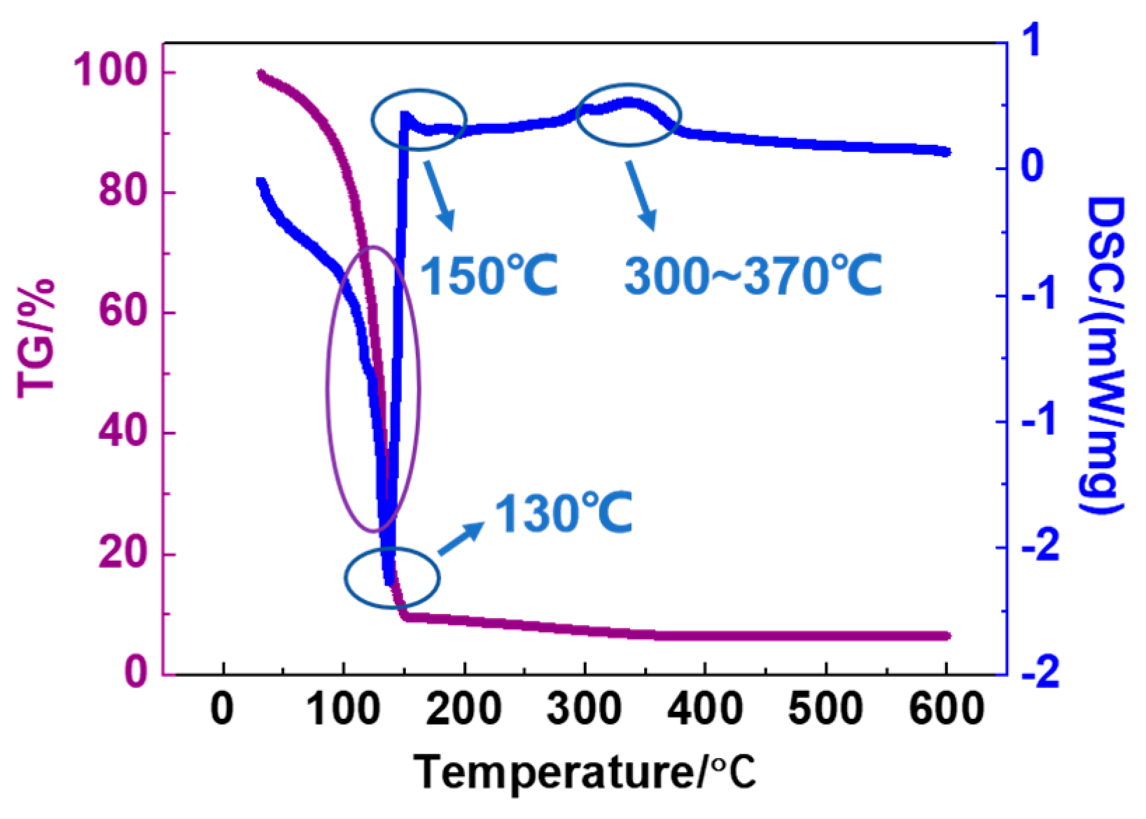
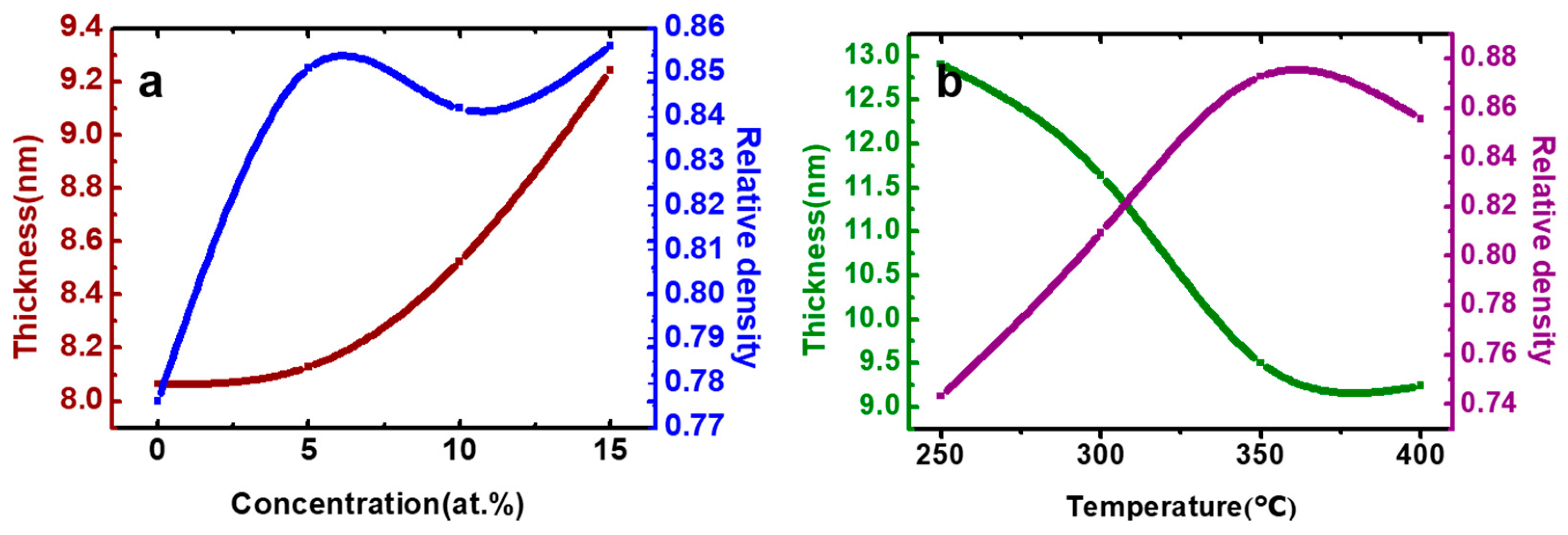
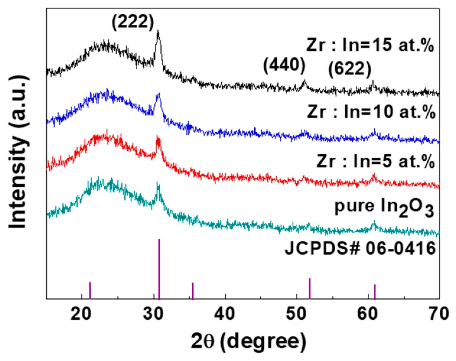
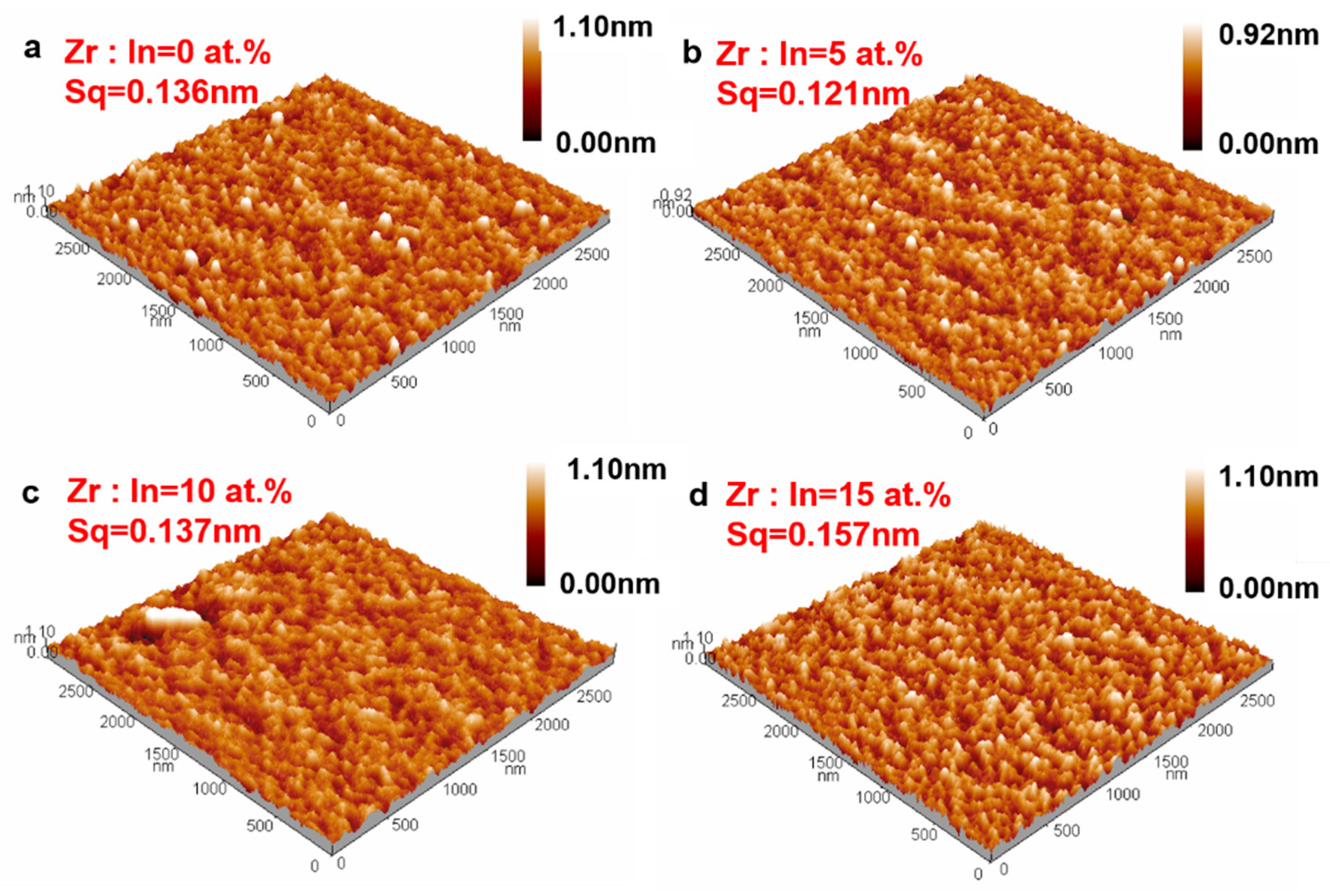
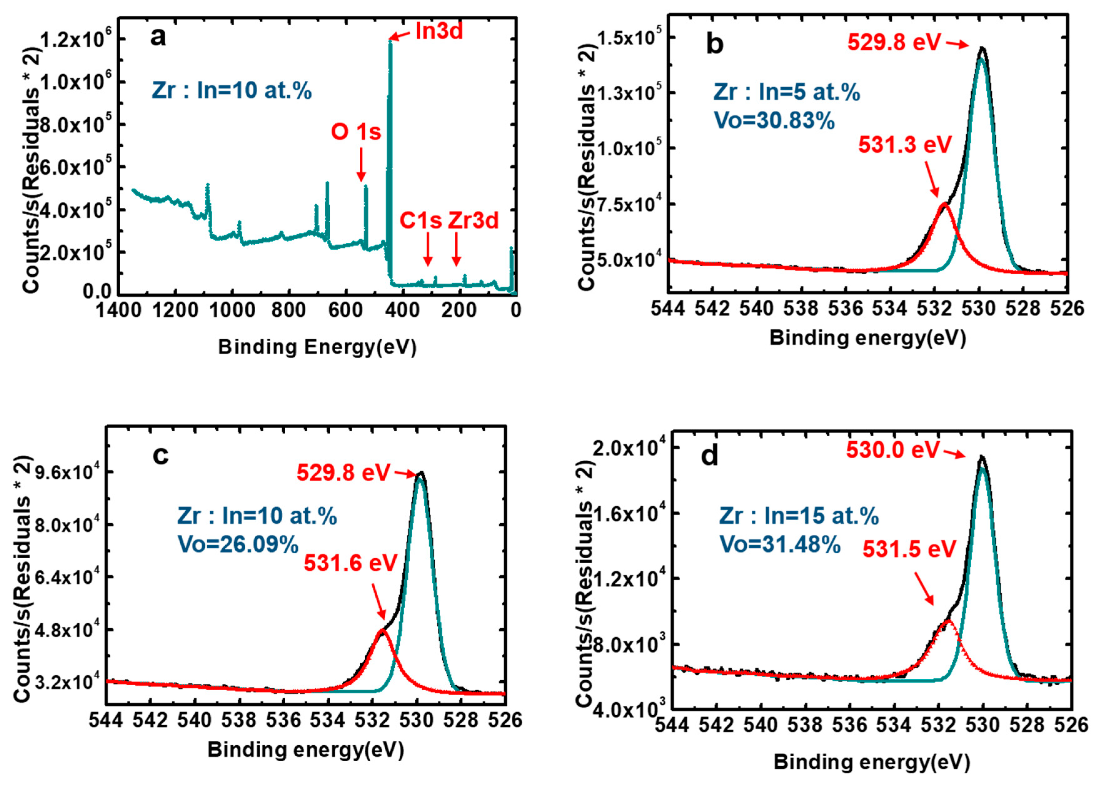
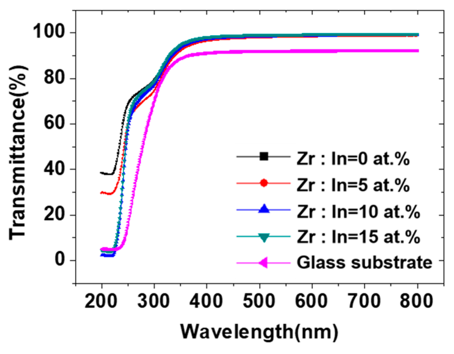
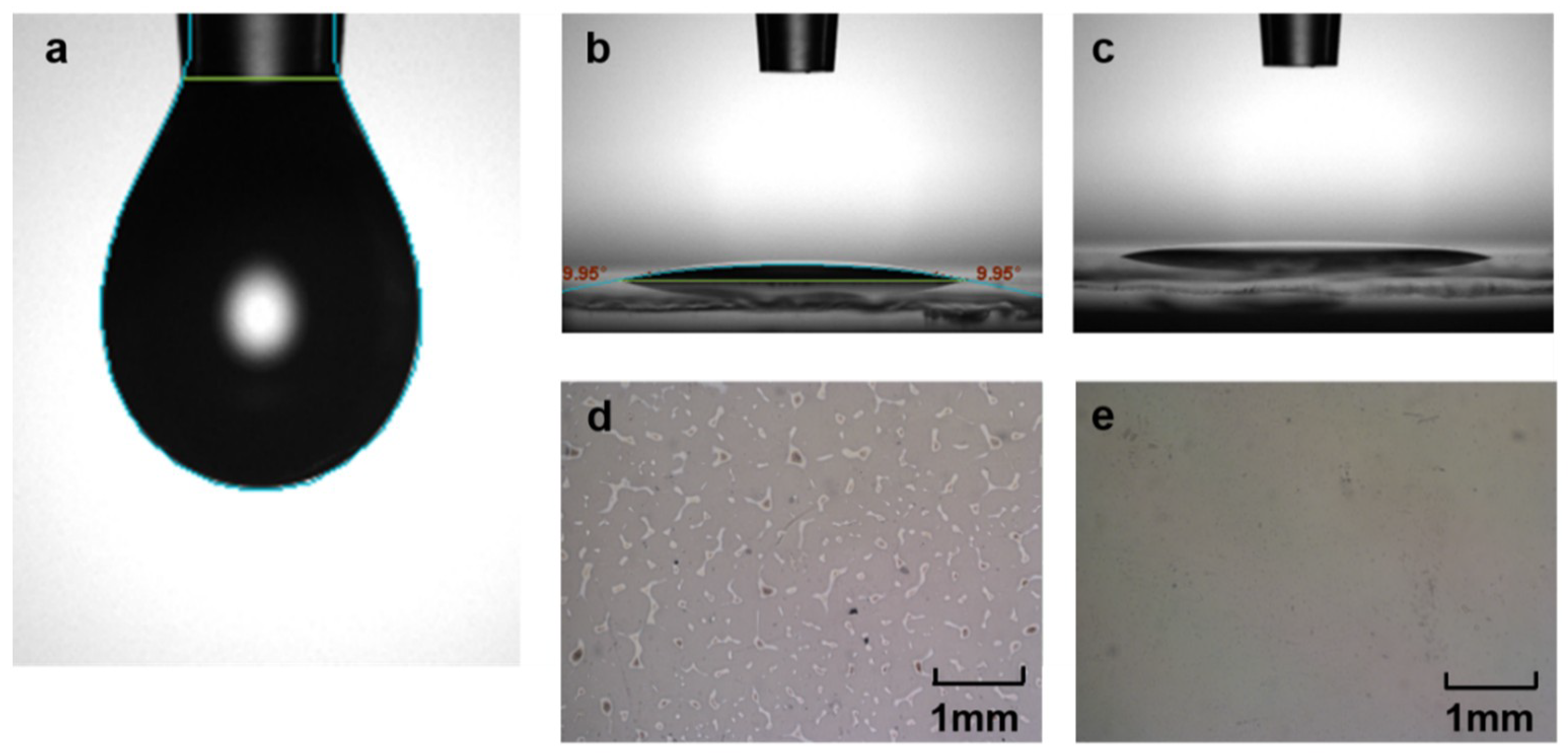
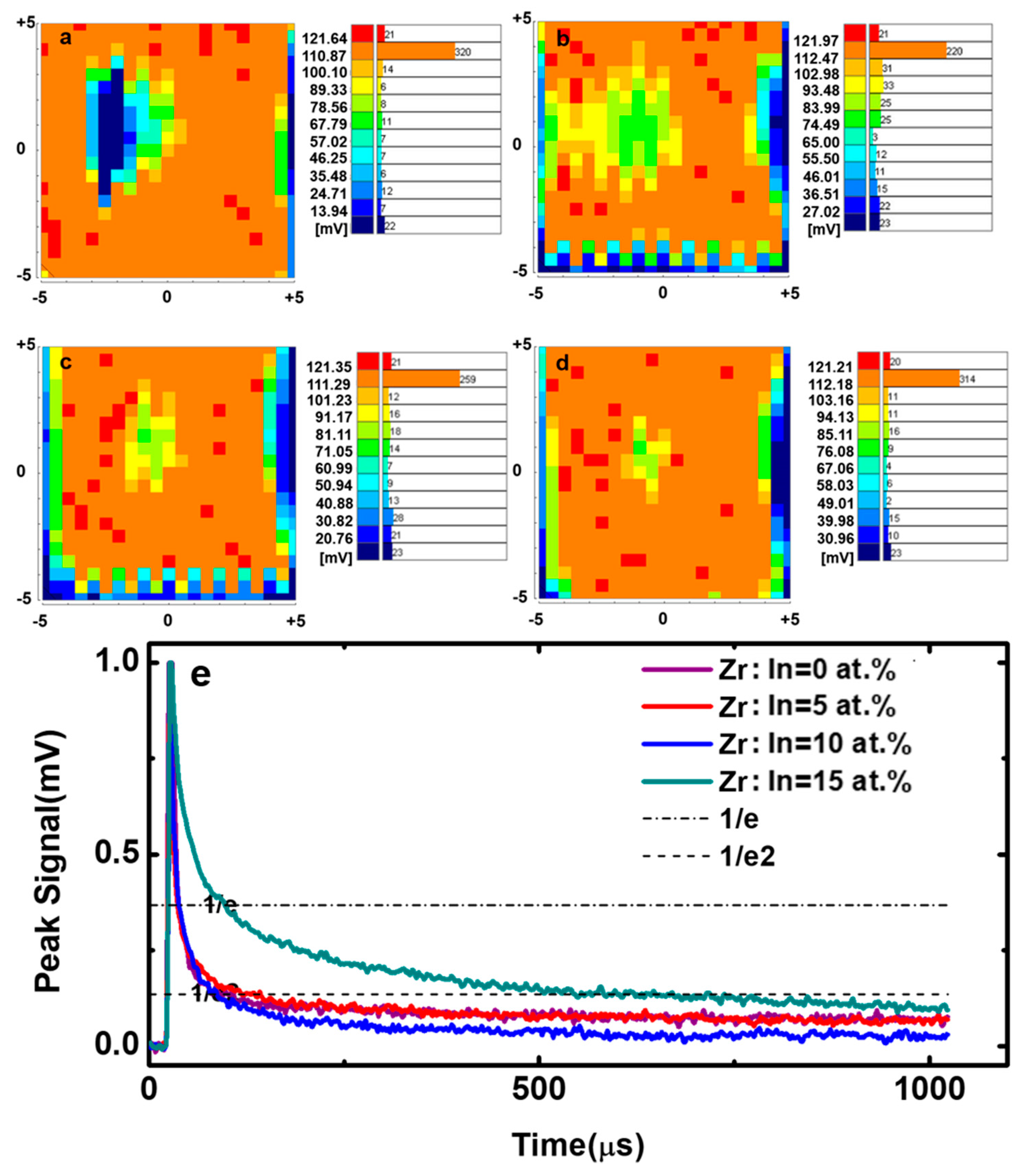
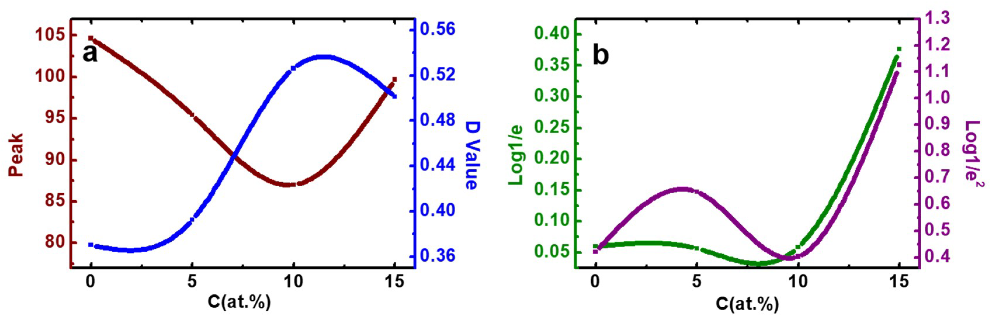
3. Results and Discussion

The surface tension of the InxZryO solution is shown in Figure 1a. When the droplet volume was 7.85 μL, the solution exhibited a surface tension of 30.82 mN/m. In order to improve the surface hydrophilicity of the glass substrate and then improve the surface topography of the coated InxZryO thin film, UV treatment was carried out on the substrate before spin coating. UV treatment was used to remove the surface contaminants and increase the number of the surface dangling bonds, which improved the uniformity of the thin films. As shown in Figure 1b,c, the contact angle formed by the precursor droplet was smaller after the UV treatment of the glass substrate. As shown in Figure 1d,e, the deposited film showed poor uniformity due to the small surface energy of the substrate without UV treatment, while the UV-treated one was more uniform and had better morphology.
The thermogravimetry-differential scanning calorimetry (TG-DSC) of the InxZryO solution with different Zr contents (Zr:In = 0, 5, 10, and 15 at.%) was measured, and the curves with different Zr contents were roughly the same. Figure 2 shows the TG-DSC curves of the InxZryO solution (Zr:In = 15 at.%). The DSC curve shows an endothermic peak at about 130 °C, which is related to the boiling point of the solvent. The decline of the TG curve also illustrates this point. It was determined that the annealing temperature of InxZryO films should be higher than 130 °C. The exothermic peak located at about 150 °C can be explained by the bonding of metal and oxygen, and the metal oxide begins to form a grid structure. The exothermic peak located at 300–370 °C can be attributed to the crystallization of In2O3.
The density, thickness, and uniformity of the films are closely related to the annealing temperature and the doping concentration of zirconium. The annealing temperatures were set as 250, 300, 350, and 400 °C, and the doping concentrations of zirconium were set as 0, 5, 10, and 15 at.%. The thickness and density of the thin films were measured with XRR, as shown in Table 1. The relative density (q) is calculated by the relation:
q = ρ ρ 1 ρ 2 ,
where ρ is the density measured by XRR, ρ1 is the bulk density, and ρ2 is the density of air in this case.
The influence of the zirconium doping concentration and annealing temperature on the thin film thickness and density was analyzed. It can be seen from Figure 3a that the thickness and the relative density increased with the increase of the zirconium doping concentration. It can be observed from Figure 3b that the thickness of the thin film decreased with the increase of the annealing temperature. The relative density of thin film increased to a peak value around 350 °C, then decreased, which can be associated with high temperature removing the impurities in thin film.
Figure 4 shows the XRD spectra of InxZryO films with different Zr contents (Zr:In = 0, 5, 10, and 15 at.%) at the annealing temperature of 400 °C. As can be seen from the figure, for pure In2O3, there were corresponding peaks at (222), (440), and (622), and the intensity of the (222) diffraction peak was the highest. With doping with Zr, it was found that the (222) peak shifted to the right, indicating the gradual substitution of In3+ by Zr4+. With the increase of Zr doping concentration, the diffraction peaks at (222), (440), and (622) became higher, indicating an increased transformation from amorphous phase into crystalline phase, which is due to the strong binding ability of Zr to oxygen (Zr–O: 776 KJ/mol). Zr doping is beneficial to the oxidation and crystallization of In2O3 films annealed at 400 °C.
According to the results of XRR and XRD, large relative density of the film and crystallization occurred at 400 °C. For the semiconductor layer, the appearance of the crystal state is beneficial for improving electrical properties. Therefore, the investigation data at 400 °C are displayed when discussing the following experiment results.
To investigate the influence of the different zirconium doping concentrations (Zr:In = 0, 5, 10, and 15 at.%) at 400 °C on the surface morphology of InxZryO thin films, atomic force microscopy (AFM) was used. The scanning area of the images was 3.0 × 3.0 μm2. Figure 5 shows AFM images of InxZryO thin films with different Zr concentrations, and it can be seen that all samples show a relatively smooth morphology without cracks.
Root mean square (Sq) is used to describe the surface morphology, which is the standard deviation of the height in a testing area. The surface roughness of the thin film might increase when adding zirconium atoms into the precursor solution. However, because the In2O3 films are doped with a trace of Zr, the surface roughness of the thin film is only slightly affected. The Sq of a pure In2O3 film is 0.136 nm, and the value changed to 0.121 and 0.137 nm for the films of Zr:In = 5 and 10 at.%, respectively. When the Zr doping concentration was 15 at.%, the Sq value of the thin film (0.157 nm) was the highest.
X-ray photoelectron spectra (XPS) were used to confirm the chemical structure and composition of the In2O3 thin film doped with different concentrations of Zr annealed at 400 °C. The presence of In, O, C, and Zr elements can all be confirmed by the XPS spectra shown in Figure 6a, also, impurity elements such as N were not detected, which indicates that the residual solvent was basically removed. According to the spectral peak information, the doping ratio of zirconium in four different samples was basically in line with expectations.
Figure 6b–d shows the peak separation result of O 1s, and it can be generally divided into two different near-Gaussian subpeaks. The major peak at around 529.8 eV is attributed to the bonding of oxygen and metal ions (M–O), and the peak located at around 531.5 eV is assigned to oxygen atoms near the oxygen vacancy. The relative quantity of oxygen vacancies under the four doping ratios are shown in Table 2.
Further, the influence of the annealing temperature and the zirconium doping concentration on the quality and properties of InxZryO active layer films was investigated by the microwave photoconductivity decay (μ-PCD) method. Samples manufactured under different annealing temperatures were respectively tested, and it was found that the InxZryO thin film manufactured at 400 °C showed optimal properties. Table 3 shows the properties of In2O3 thin film with different doping concentrations of zirconium tested by μ-PCD.
Figure 7a–d shows the μ-PCD mapping scan of the In2O3 thin film with different Zr doping ratios (Zr:In = 0, 5, 10, and 15 at.%) annealed at 400 °C. The reflectivity peak signal of μ-PCD correlated with the shallow local defect state concentration of the oxide and varied with the composite rate of photo-generated carriers, so it has important significance for us to study the mobility and concentration of carriers. The overall homogeneity of carriers in InxZryO films obtained by spin coating was good. However, the small centripetal force in the middle of the substrate may be a major reason that leads to less carrier distribution in the spin coating process. Meanwhile, the average value of the carrier peak value measured was lager, indicating that the InxZryO films had good quality and electrical properties.
As can be seen from Figure 8a, with the increase of the doping concentration of zirconium, the peak reflectivity signal first gradually decreased. When the doping concentration increased to 10 at.%, the peak value reached the minimum, and then increased. Along with the increase of the zirconium doping ratio, the peak value decreased first and then increased mainly depending on the following two effects: (1) The difference of electron negativity between Zr (1.4) and O (3.5) is larger than the difference between In (1.7) and O, hence, the combination ability of Zr with O is stronger. So, doping with Zr will more effectively inhibit the production of oxygen vacancies, leading to the decrease of carrier concentration. However, such inhibition will reach a saturation point with an increasing concentration of Zr. It can be seen from Table 2 that the relative quantity of oxygen vacancies first decreased with the increase of doping concentration, and then increased again when the doping concentration reached 15 at.%. This leads to the carrier concentration decreasing first and then increasing with the Zr doping concentration in the film increasing from 0 to 15 at.%. (2) The main quantum number of zirconium is large. The 2p orbital of the oxygen ion is small, while the ns orbital of zirconium has a high propagation speed in space. This increases the probability of the overlapping of ns orbitals of adjacent zirconium ions, forming a wider conduction band and improving the mobility of electrons. Under the influence of these two aspects, the peak value of the minority carrier measured by μ-PCD showed the above variation to the rule. Additionally, with the increase of the Zr doping concentration, the uniformity of the carriers improved, which can be seen from Figure 7.
Another important measurement parameter in μ-PCD is the D value, which reflects the situation of trapping and the recombination center [35]. A high D value indicates that the shallow localized state density of carrier trapping or the release center in the middle band gap region of the film is small, and the device has better stability. With the increase of the doping concentration of zirconium, the D value showed an increasing trend, indicating that the small doping of zirconium reduced the density of the defect state. It is related to the higher chemical bond energy of the combination of zirconium and oxygen.
The lifetime of carriers in the photoconductor is mainly related to fast decay time (τ1) and slow decay time (τ2), the variation of fast decay time and slow decay time at different zirconium doping ratios is shown in Figure 7e and Figure 8b. Among them, fast decay time is related to the carrier recombination processes of the deep localized states [33]. The longer carrier lifetime is related to the carrier being captured in the defect states for some time and then released. So, as the zirconium doping ratio increases, the density of the deep localized defect states increases. Slow decay time is related to the defect of the shallow localized states concentration. As the zirconium doping ratio increases, the defect of the shallow localized states concentration also increases.
Based on these results it can be concluded that the relative number of oxygen vacancies and the minority carrier concentration decrease with the increase of the Zr doping concentration up to 10 at.%. Hence, the strongest inhibition effect on the generation of oxygen vacancies (Vo = 26.09%) is achieved at this doping concentration for InxZryO thin films annealed at 400 °C.
Figure 9 reveals that the InxZryO thin films spin coated on the glass substrate annealed at 400 °C presented a transmittance over 93% in the wavelength range of visible light. The results show that zirconium doping did not affect the transparency of In2O3 films, indicating that the InxZryO active layer can be applied to transparent devices.

4. Conclusions

In summary, we prepared InxZryO films by the solution method on UV-treated substrates. μ-PCD was used to evaluate the quality of the InxZryO thin films by analyzing the response of the thin films under laser irradiation as a noncontact and nondestructive technique. The results show that Zr doping makes the film less defective, gives longer carrier life, and improves the relative density of films. The number of oxygen vacancies reaches the minimum value, Vo = 26.09%, in the case of InxZryO films with 10 at.% Zr doping concentration, annealed at 400 °C. These features and the good transmittance in the visible domain recommend the prepared InxZryO films as active layer materials for the preparation of high-performance TFT devices.

Author Contributions

Conceptualization, J.Z., H.N., and R.Y.; Formal Analysis, S.Z., D.G., and J.P.; Investigation, X.F., Y.W., Z.L., and J.P.; Writing—Original Draft, X.F., S.Z., W.C., and R.Y.; Writing—Review and Editing, J.Z. and H.N.

Funding

This work was supported by the National Natural Science Foundation of China (No. 51771074), the Guangdong Science and Technology Project (No. 2016B090907001), the 2019 Guangdong University Student Science and Technology Innovation Special Fund (“Climbing Plan” Special Fund) (Nos. pdjh2019a0028 and pdjh2019b0041), the National College Students’ Innovation and Entrepreneurship Training Program (No. 201910561005), the South China University of Technology 100 Step Ladder Climbing Plan Research Project (No. j2tw201902475), and the Fundamental Research Funds for the Central Universities.

Conflicts of Interest

The authors declare no conflict of interest.

References

  1. Xu, W.; Hu, L.; Zhao, C.; Zhang, L.; Zhu, D.; Cao, P.; Liu, W.; Han, S.; Liu, X.; Jia, F.; et al. Low temperature solution-processed IGZO thin-film transistors. Appl. Surf. Sci. 2018, 455, 554–560. [Google Scholar] [CrossRef]
  2. Chen, R.; Lan, L. Solution-processed metal-oxide thin-film transistors: A review of recent developments. Nanotechnology 2019, 30, 312001. [Google Scholar] [CrossRef] [PubMed]
  3. Hoang, H.; Hori, T.; Yasuda, T.-O.; Kizu, T.; Tsukagoshi, K.; Nabatame, T.; Trinh, B.N.Q.; Fujiwara, A. Si-doping effect on solution-processed In-O thin-film transistors. Mater. Res. Express 2019, 6, 026410. [Google Scholar] [CrossRef]
  4. Li, J.; Zhou, Y.-H.; Zhu, W.-Q.; Zhang, J.-H.; Zhang, Z.-L. Combustion synthesis of nontoxic water-induced InYO thin film and application in thin film transistor. Mater. Sci. Semicond. Process. 2019, 93, 201–207. [Google Scholar] [CrossRef]
  5. Kang, L.; An, H.; Jung, S.; Kim, S.; Nahm, S.; Kim, D.-G.; Lee, C.G. Low-voltage operating solution-processed CdS thin-film transistor with Ca2Nb3O10 nanosheets deposited using Langmuir-Blodgett method for a gate insulator. Appl. Surf. Sci. 2019, 476, 374–377. [Google Scholar] [CrossRef]
  6. Ren, J.; Li, K.; Yang, J.; Lin, D.; Kang, H.; Shao, J.; Fu, R.; Zhang, Q. Solution-processed amorphous gallium-tin oxide thin film for low-voltage, high-performance transistors. Sci. China-Mater. 2019, 62, 803–812. [Google Scholar] [CrossRef]
  7. Ha, H.; Hori, T.; Yasuda, T.O.; Kizu, T.; Tsukagoshi, K.; Nabatame, T.; Trinh, B.N.Q.; Fujiwara, A. Investigation on solution-processed In-Si-O thin-film transistor via spin-coating method. In Proceedings of the 2018 25th International Workshop on Active-Matrix Flatpanel Displays and Devices (AM-FPD), Kyoto, Japan, 3–6 July 2018. [Google Scholar]
  8. Lee, J.; Lee, J.; Park, J.; Lee, S.-E.; Lee, E.G.; Im, C.; Lim, K.-H.; Kim, Y.S. Solution-grown homojunction oxide thin-film transistors. ACS Appl. Mater. Interfaces 2019, 11, 4103–4110. [Google Scholar] [CrossRef]
  9. Hwang, N.; Lim, Y.; Lee, S.; Lee, J.S.; Yi, M. Solution based indium zinc oxide thin film transistor with diffused aluminum oxide insulator layer. In Proceedings of the 2018 International Conference on Electronics, Information, and Communication (ICEIC), Honolulu, HI, USA, 24–27 January 2018; pp. 1–3. [Google Scholar]
  10. Lee, W.Y.; Jang, B.; Lee, S.; Kim, T.; Jang, J. High performance sol-gel processed SnO2 thin film transistor with sol-gel processed ZrO2 layers. In Proceedings of the 2018 25th International Workshop on Active-Matrix Flatpanel Displays and Devices (AM-FPD), Kyoto, Japan, 3–6 July 2018. [Google Scholar]
  11. Cai, W.; Wilson, J.; Zhang, J.; Park, S.; Majewski, L.; Song, A. Low-voltage, flexible InGaZnO thin-film transistors gated with solution-processed, ultra-thin AlxOy. IEEE Electron Device Lett. 2019, 40, 36–39. [Google Scholar] [CrossRef]
  12. Jeon, J.-Y.; Ha, T.-J. Improvement in interfacial characteristics of low-voltage carbon nanotube thin-film transistors with solution-processed boron nitride thin films. Appl. Surf. Sci. 2017, 413, 118–122. [Google Scholar] [CrossRef]
  13. Kang, J.K.; Park, S.P.; Na, J.W.; Lee, J.H.; Kim, D.; Choi, J.S.; Kim, H.J. Fabrication of eco-friendly solution-processed indium zinc oxide thin-film transistors through recycling based on photocatalytic reactions of TiO2. SID Symp. Dig. Tech. Pap. 2018, 49, 1264–1267. [Google Scholar] [CrossRef]
  14. Hong, J.-Y.; Shin, K.-H.; Yoon, D.G.; Chin, B.D.; Kim, S.H. All-solution-processed, flexible thin-film transistor based on PANI/PETA as gate/gate insulator. RSC Adv. 2015, 5, 105785–105788. [Google Scholar] [CrossRef]
  15. Kim, H.J.; Kim, Y.G.; Park, S.P.; Kim, D.; Kim, N.E.; Choi, J.S.; Kim, H.J. Self-pattern process of InZnO thin-film transistors using photosensitive precursors. SID Symp. Dig. Tech. Pap. 2017, 48, 180–182. [Google Scholar] [CrossRef]
  16. Rim, Y.S.; Keum, M.-J.; Baek, Y.; Lee, B.M.; Kim, K.H. Film Density Controlled-InGaZnO multi-stacked channel based thin-film transistors using a solution process. Sci. Adv. Mater. 2017, 9, 1578–1582. [Google Scholar] [CrossRef]
  17. Choi, H.-S.; Cho, W.-J. Controlling In-Ga-Zn-O thin-film resistance by vacuum rapid thermal annealing and application to transparent electrode. Phys. Status Solidi A 2019, 216, 1800653. [Google Scholar] [CrossRef]
  18. Nguyen, M.-C.; Nguyen, A.H.-T.; Ji, H.; Cheon, J.; Kim, J.-H.; Yu, K.-M.; Cho, S.-Y.; Kim, S.-W.; Choi, R. Application of single-pulse charge pumping method on evaluation of indium gallium zinc oxide thin-film transistors. IEEE Trans. Electron Devices 2018, 65, 3786–3790. [Google Scholar] [CrossRef]
  19. Xia, Z.; Lu, L.; Li, J.; Kwok, H.S.; Wong, M. The use of fluorination to enhance the performance and the reliability of elevated-metal metal-oxide thin-film transistors. SID Symp. Dig. Tech. Pap. 2018, 49, 1235–1238. [Google Scholar] [CrossRef]
  20. Kim, K.S.; Ahn, C.H.; Kang, W.J.; Cho, S.W.; Jung, S.H.; Yoon, D.H.; Cho, H.K. An all oxide-based imperceptible thin-film transistor with humidity sensing properties. Materials 2017, 10, 530. [Google Scholar] [CrossRef] [PubMed]
  21. Meng, Y.; Liu, A.; Guo, Z.; Liu, G.; Shin, B.; Noh, Y.-Y.; Fortunato, E.; Martins, R.; Shan, F. Electronic devices based on oxide thin films fabricated by fiber-to-film process. ACS Appl. Mater. Interfaces 2018, 10, 18057–18065. [Google Scholar] [CrossRef] [PubMed]
  22. Wan, D.; Abliz, A.; Su, M.; Liu, C.; Jiang, C.; Li, G.; Chen, H.; Guo, T.; Liu, X.; Liao, L. Low-frequency noise in high-mobility a-InGaZnO/InSnO nanowire composite thin-film transistors. IEEE Electron Device Lett. 2017, 38, 1540–1542. [Google Scholar] [CrossRef]
  23. Lee, S.H.; Oh, D.J.; Hwang, A.Y.; Park, J.W.; Jeong, J.K. High performance a-InZnSnO thin-film transistor with a self-diffusion-barrier formable copper contact. Thin Solid Films 2017, 637, 3–8. [Google Scholar] [CrossRef]
  24. Pan, T.-M.; Peng, B.-J.; Her, J.-L.; Lou, B.-S. Effect of In and Zn content on structural and electrical properties of InZnSnO thin-film transistors using an Yb2TiO5 gate dielectric. IEEE Trans. Electron Devices 2017, 64, 2233–2238. [Google Scholar] [CrossRef]
  25. Wang, Y.; Su, J.; Dai, S.; Li, R.; Ma, Y.; Wang, Q.; Tian, L.; Ning, K.; Zhang, X. Double active layer InZnO:N/InZnSnO thin film transistors with high mobility at low annealing temperature. J. Mater. Sci.-Mater. Electron. 2019, 30, 1496–1499. [Google Scholar] [CrossRef]
  26. Yang, J.-W.; Na, Y.-B.; Shin, J.-H.; Hong, C.-H.; Seo, W.-H.; Kim, K.-H.; Song, C.-W.; Song, S.-H.; Kwon, H.-I.; Cheong, W.-S. Effects of Er-doping on amorphous InZnSnO/InZnSnO: Er double-channel thin-film transistors. J. Nanosci. Nanotechnol. 2017, 17, 3415–3419. [Google Scholar] [CrossRef]
  27. Liu, H.-Y.; Hung, C.-C.; Hsu, W.-C. Deposition of oxide thin films by ultrasonic spray pyrolysis deposition for InGaZnO thin-film transistor applications. IEEE Electron Device Lett. 2018, 39, 1520–1523. [Google Scholar] [CrossRef]
  28. Takechi, K.; Kuwahara, Y.; Tanaka, J.; Tanabe, H. Depth-profiling XPS analysis of He-plasma treated amorphous InGaZnO thin films for use in top-gate coplanar thin-film transistors. Jpn. J. Appl. Phys. 2019, 58, 038005. [Google Scholar] [CrossRef]
  29. Wang, W.-H.; Heredia, E.; Lyu, S.-R.; Liu, S.-H.; Liao, P.-Y.; Chang, T.-C.; Jiang, P.-H. Weak localization and weak antilocalization in double-gate a-InGaZnO thin-film transistors. IEEE Electron Device Lett. 2018, 39, 212–215. [Google Scholar] [CrossRef]
  30. Yang, J.; Chang, T.-C.; Chen, B.-W.; Liao, P.-Y.; Chiang, H.-C.; Zhang, Q. Effects of mechanical stress on flexible dual-gate a-InGaZnO thin-film transistors. Phys. Status Solidi A 2018, 215, 1700426. [Google Scholar] [CrossRef]
  31. Xiao, P.; Dong, T.; Lan, L.; Lin, Z.; Song, W.; Song, E.; Sun, S.; Li, Y.; Gao, P.; Luo, D. High-mobility flexible thin-film transistors with a low-temperature zirconium-doped indium oxide channel layer. Phys. Status Solidi (RRL) Rapid Res. Lett. 2016, 10, 493–497. [Google Scholar] [CrossRef]
  32. Zhang, X.; Liu, X.; Ning, H.; Yuan, W.; Deng, Y.; Zhang, X.; Wang, S.; Wang, J.; Yao, R.; Peng, J. Characterization studies of the structure and properties of Zr-doped SnO2 thin films by spin-coating technique. Superlattices Microstruct. 2018, 123, 330–337. [Google Scholar] [CrossRef]
  33. Liu, X.; Cai, W.; Chen, J.; Fang, Z.; Ning, H.; Hu, S.; Tao, R.; Zeng, Y.; Zheng, Z.; Yao, R.; et al. A novel nondestructive testing method for amorphous Si–Sn–O films. J. Phys. D Appl. Phys. 2016, 49, 505102. [Google Scholar] [CrossRef]
  34. Yao, R.; Zheng, Z.; Xiong, M.; Zhang, X.; Ning, H.; Fang, Z.; Xie, W.; Lu, X.; Peng, J. Low-temperature fabrication of sputtered high-k HfO2 gate dielectric for flexible a-IGZO thin film transistors. Appl. Phys. Lett. 2018, 112, 103503. [Google Scholar] [CrossRef]
  35. Wei, J.; Fang, Z.; Peng, J.; Cai, W.; Zhu, Z.; Yao, R.; Zhou, S.; Yuan, W.; Lu, K.; Ning, H. High-performance spin-coated aluminum oxide dielectric fabricated by a simple oxygen plasma-treatment process. J. Phys. D Appl. Phys. 2018, 51, 365101. [Google Scholar] [CrossRef]
Figure 1. (a) The surface tension of InxZryO precursor solution. (b) Contact angle of precursor solution on the glass substrate without UV treatment. (c) Contact angle of precursor solution on the glass substrate with UV treatment. (d) Top view of InxZryO film on glass substrate without UV treatment. (e) Top view of InxZryO film on glass substrate with UV treatment.
Coatings 09 00426 g001
Figure 2. Thermal behavior of InxZryO precursor solution (Zr:In = 15 at.%) analyzed by thermogravimetry-differential scanning calorimetry (TG-DSC).
Coatings 09 00426 g002
Figure 3. (a) Thickness and relative density changes with the Zr doping concentration annealed at 400 °C. (b) Thickness and relative density changes with the annealing temperature at 15 at.% Zr doping concentration.
Coatings 09 00426 g003
Figure 4. X-ray diffraction (XRD) patterns of the InxZryO films with different Zr contents (Zr:In = 0, 5, 10, and 15 at.%) annealed at 400 °C.
Coatings 09 00426 g004
Figure 5. Atomic force microscopy (AFM) 3D images (3.0 × 3.0 μm2) of InxZryO thin films at 400 °C with different Zr doping concentrations, (ad): Zr:In = 0, 5, 10, and 15 at.%, respectively.
Coatings 09 00426 g005
Figure 6. X-ray photon spectroscopy (XPS) spectra: (a) Overview scans of sample. (bd) O 1s for the solution-processed indium oxide thin films with different Zr doping concentrations (Zr:In = 5, 10, and 15 at.%).
Coatings 09 00426 g006
Figure 7. The result of microwave photoconductivity decay (μ-PCD) mapping scan of In2O3 thin films when the Zr doping ratio was (a) 0 at.%, (b) 5 at.%, (c) 10 at.%, and (d) 15 at.%. (e) μ-PCD decay curves.
Coatings 09 00426 g007
Figure 8. (a) Peak and D value changes with the Zr doping concentrations under 400 °C. (b) Log1/e and Log1/e2 changes with the Zr doping concentrations under 400 °C.
Coatings 09 00426 g008
Figure 9. Transmittance of different doping ratio films changes with the wavelength under 400 °C.
Coatings 09 00426 g009
Table 1. Measurement results of In2O3 thin film with different doping concentrations of zirconium and different temperatures.
Zr Doping Concentration
(at.%)
Temperature
(°C)
Thickness
(nm)
Density
( ρ )   ( g / cm 3 )
Bulk Density
( ρ 1 )   ( g / cm 3 )
Relative Density
(q)
04008.0655.5747.1790.776
58.1306.0517.1130.851
108.5255.9307.0460.842
159.2445.9726.9800.856
1525012.9105.1876.9800.743
30011.6425.6500.809
3509.5046.0930.873
4009.2445.9720.856
Table 2. The relative quantity of oxygen vacancies varied with the Zr doping concentrations.
Zr Doping Concentration (at.%)Relative Quantity of Oxygen Vacancies (%)
041.78
530.83
1026.09
1531.48
Table 3. Properties of In2O3 thin film with different doping concentrations of zirconium tested by μ-PCD.
Zr Doping Concentration
(at.%)
Peak Mean (mV)D Valueτ1 (μs)τ2 (μs)
0104.70.37020.05930.4207
595.40.39250.05620.6472
1087.00.52630.05860.4034
1599.70.50120.37611.1260

