Article

Optical Characterization of Non-Stoichiometric Silicon Nitride Films Exhibiting Combined Defects

1
Department of Physical Electronics, Faculty of Science, Masaryk University, Kotlářská 2, 611 37 Brno, Czech Republic
2
Institute of Physical Engineering, Brno University of Technology, Technická 2, 616 69 Brno, Czech Republic
*
Author to whom correspondence should be addressed.
Coatings 2019, 9(7), 416; https://doi.org/10.3390/coatings9070416
Submission received: 31 May 2019 / Revised: 21 June 2019 / Accepted: 26 June 2019 / Published: 28 June 2019

Abstract

:
The study was devoted to optical characterization of non-stoichiometric silicon nitride films prepared by reactive magnetron sputtering in argon-nitrogen atmosphere onto cold (unheated) substrates. It was found that these films exhibit the combination of three defects: optical inhomogeneity (refractive index profile across the films), uniaxial anisotropy with the optical axis perpendicular to the boundaries and random roughness of the upper boundaries. The influence of the uniaxial anisotropy was included into the corresponding formulae of the optical quantities using the matrix formalism and the approximation of the inhomogeneous layer by a multilayer system consisting of large number thin homogeneous layers. The random roughness was described using the scalar diffraction theory. The processing of the experimental data was performed using the multi-sample modification of the least-squares method, in which experimental data of several samples differing in thickness were processed simultaneously. The dielectric response of the silicon nitride films was modeled using the modification of the universal dispersion model, which takes into account absorption processes corresponding to valence-to-conduction band electron transitions, excitonic effects and Urbach tail. The spectroscopic reflectometric and ellipsometric measurements were supplemented by measuring the uniformity of the samples using imaging spectroscopic reflectometry.

1. Introduction

Silicon nitride thin films are intensively utilized in practice. They are employed as antireflection coatings in silicon solar cells because of their suitable optical properties owing to the silicon optical properties (see, e.g., [1,2,3,4]). Silicon nitride films also exhibit appropriate properties of passivation on silicon surfaces (see, e.g., [5,6]). They are utilized as passivation layers and masks for local oxidation of silicon surfaces and optical waveguides. Non-stoichiometric silicon nitride (SiN x ) films have been employed as inhomogeneous films for creating optical filters [7]. The SiN x films, which are silicon-rich, have utilization in many other applications. For example, these films are utilized in memory devices [8], photonic devices [9] and membranes for micromechanical devices [10]. For many practical applications, it is important to know the optical properties of stoichiometric (Si 3 N 4 ) and non-stoichiometric SiN x films. Therefore, considerable attention has been devoted to the optical characterization of these films so far.
From the papers published, one can see that the optical constants of the SiN x are strongly dependent on technological conditions of their preparation. This statement is true for the SiN x rich in silicon in particular. Thus, individual methods or approaches must be used to characterize thin films of SiN x . Correct results of the optical characterization of these films can only be achieved if true dispersion and structural models are utilized. Below, the typical results of the optical characterization of the SiN x films presented in the literature are introduced.
In [11], spectroscopic ellipsometry was employed for the optical characterization of the SiN x films deposited onto silicon single substrates in spectral range 1.5–4.0 eV. An evolution of spectral dependencies of their refractive index was investigated in dependency on stoichiometric ratio of Si and Si 3 N 4 . It was stated that the refractive index is a precise indicator of the composition of the studied SiN x films. For determining the refractive index spectral dependencies, the Farouhi–Bloomer dispersion model was used. This model is problematic from the physical point of view since it lacks the time reversal symmetry and the integral in the sum rule is divergent. Moreover, this model is not Kramers–Kronig consistent if the zero absorption below the band gap is considered. In the structural model of the SiN x films investigated in [11], no defects were taken into account. Note that the films were prepared by magnetron sputtering.
In [12], the spectral dependencies of transmittance of the SiN x films prepared onto quartz substrates were measured within the spectral range 170–800 nm. Experimental data of transmittance were not processed by any dispersion model. Only the values of the band gap were determined using the Tauc relation (for details, see [12]). The dependency of the band gap values on a negative substrate bias was determined (films were prepared using radio frequency magnetron sputtering). The structural model of the SiN x films was not mentioned either. By means of an atomic force microscope, it was found that the upper boundaries of the films exhibited very fine random roughness in values of several Angstroms.
In [13], the optical characterization of the SiN x prepared by plasma-enhanced chemical vapor deposition (PECVD) was performed by the processing experimental data obtained by spectroscopic ellipsometry applied at incidence angle of 65 within the spectral range 245–800 nm. Experimental data achieved using variable angle of incidence ellipsometry applied for several wavelengths from the visible range together with reflectance measured for wavelength of 248 nm at normal incidence were also used for the optical characterization of the SiN x films. The processing of the experimental data was based on expression of the optical constants of these films by means of effective medium approximation (EMA). By means of the EMA, an isotropic mixture consisting of three components, i.e., amorphous Si 3 N 4 , amorphous Si and voids, was created. This mixture served as an effective material of the SiN x films studied. In this paper, the spectral dependencies of the optical constants of these components are considered to be known. This means that no dispersion model was assumed. Then, the values of thickness, optical constants and relative volume of amorphous silicon in SiN x films were determined for different technological conditions. A structural model utilized at the optical characterization of these films was not presented either.
In [14], the realistic Tauc–Lorentz dispersion model was used to fit data of spectroscopic ellipsometry measured for SiN x films prepared by the PECVD within the spectral range 1–5.5 eV. Random roughness of the upper boundaries of these films was modeled by using the Bruggeman formula of the EMA. It was assumed that 50% voids and 50% SiN x form the effective layer representing this roughness. The thickness of this effective layer together with spectral dependencies of the optical constants and thickness of the SiN x films were determined. It should be emphasized that the description of random roughness by the Bruggeman formula is not too suitable since the effective layer do not substitute this roughness in realistic way. The use of some theories describing an interaction of light and random roughness more exactly than the EMA such as the Rayleigh–Rice theory or scalar diffraction theory is much better from the physical point of view (see, e.g., [15,16,17,18,19,20,21,22,23]). Other defects were not considered in [14].
In this study, the optical characterization of the samples of the amorphous SiN x films prepared by reactive magnetron sputtering onto silicon single substrates was performed. These films exhibit three defects, i.e., inhomogeneity represented by profiles of the optical constants across the films, artificial optical anisotropy in the optical constants corresponding to uniaxial anisotropy with the optical axis perpendicular to the boundaries and random roughness of the upper boundaries. A new, very complicated and efficient method of the optical characterization of these films had to be developed. The application of this method for practical purposes is illustrated by means of characterizing three samples of these films. On the basis of the results achieved for these samples, the practical usefulness of the method is presented.

2. Theory

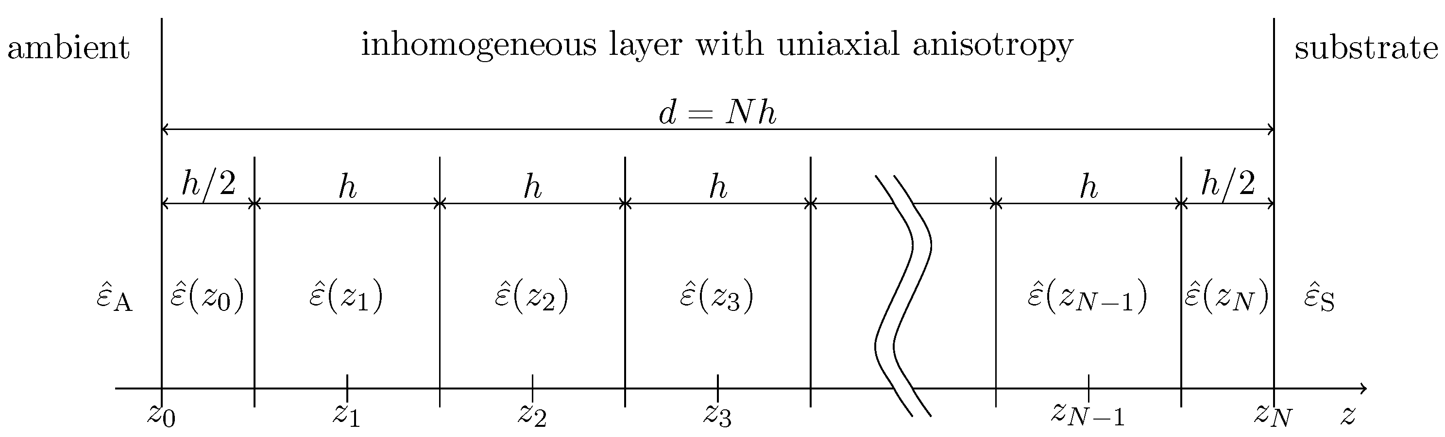
2.1. Structural Model

By means of X-ray diffraction measurements, it was found that the non-stoichiometric silicon nitride films (SiN x ) studied here were amorphous. The simultaneous processing of experimental data obtained by variable angle spectroscopic ellipsometry and spectroscopic reflectometry showed that formulae for the optical quantities corresponding to the thin film model without any defects could not be utilized. It was evident because fits achieved by this simultaneous processing of ellipsometric and reflectometric data were very poor. Differences between the experimental and theoretical data were too large. However, if the ellipsometric and reflectometric data were processed separately, better fits were achieved for each of these data. This indicates that the characterized films exhibited some defects. To our experience, inhomogeneity of the optical constants of the SiN x films often occurs. Therefore, the inhomogeneity in the optical constants across the films was assumed. In other words, it was assumed that the refractive index and extinction coefficient changed in the direction perpendicular to the boundaries. The reality that the fits of the individual data processed separately were evidently better than the fits obtained by the simultaneous processing of the ellipsometric and reflectometric data indicated that the SiN x films could exhibit an optical anisotropy. It is known that this optical anisotropy originates if mechanical stresses occur inside the films. This anisotropy mostly corresponds to the uniaxial anisotropy with the optical axis perpendicular to the film boundaries. Therefore, such the kind of the optical anisotropy was included in our structural model of the SiN x films studied here. By using atomic force microscopy (AFM), random roughness of the upper boundaries of these films was revealed. The AFM image of the upper boundary of one selected sample proving this roughness is presented in Figure 8. After including all the three defects into the structural model of the studied SiN x films, good fits of the ellipsometric and reflectometric data were achieved when their simultaneous processing was performed (see below).
Thus, the structural model of the SiN x films utilized in this work is specified as follows:
  • The ambient is formed by vacuum with the refractive index equal to unity.
  • The substrate is silicon single crystal wafer, i.e., the substrate is optically homogeneous and isotropic.
  • The films are uniform in thickness inside the areas used for spectrophotometric and ellipsometric measurements.
  • The non-stoichiometric silicon nitride thin films are inhomogeneous with profiles of the optical constants across these films.
  • These films exhibit uniaxial anisotropy with the optical axis perpendicular to the boundaries.
  • Random roughness was assumed on the upper boundaries of the films. It was assumed that this roughness corresponds to the Gaussian stochastic process.

2.2. Optical Quantities of Inhomogeneous Films

The method that was used to calculate the Fresnel coefficients of the inhomogeneous film with uniaxial anisotropy having the optical axis perpendicular to the boundaries is described in this section. The dielectric response at depth z inside the inhomogeneous film is described by the dielectric tensor
ε ^ ( z ) = ε ^ o ( z ) 0 0 0 ε ^ o ( z ) 0 0 0 ε ^ e ( z ) ,
where ε ^ o ( z ) and ε ^ e ( z ) are the ordinary and extraordinary complex dielectric functions.
The Fresnel coefficients were calculated using a method in which the inhomogeneous film was approximated by a multilayer system consisting of large number of thin homogeneous layers. The inhomogeneous film was divided by N boundaries into N + 1 layers in a manner depicted in Figure 1. The thickness of the inner layers is h = d / N , where d is the total thickness of the inhomogeneous film, while the first and the last layer have half the thickness of the inner layers. The ordinary and extraordinary dielectric functions of the individual layers were calculated as
ε ^ o , k = ε ^ o ( z k ) ,       ε ^ e , k = ε ^ e ( z k ) ,       where       z k = k d N ,
and k = 0 , 1 , 2 , , N .
The Fresnel coefficients of the layered systems can be calculated very efficiently using the matrix formalism. We present the method based on the Yeh matrix formalism [24], which was introduced to deal with layered systems containing anisotropic media. However, it should be noted that there are also other matrix formalisms usable for the special type of anisotropy considered in this paper, e.g., the transfer matrix formalism [25,26].
The junction conditions imply that the components of the wavevectors parallel to the boundaries are the same in all the layers. If the coordinate system is chosen such that z-axis is perpendicular to the boundaries and xz is the plane of incidence, then the y-components of the wavevectors vanish and the x-components are given as k x = k 0 sin θ , where k 0 = 2 π / λ is the size of the wavevector in vacuum and θ is the incidence angle in vacuum. The z-components of the wavevectors of the ordinary and extraordinary waves inside kth medium are equal to ± k ^ o z , k and ± k ^ e z , k , where
k ^ o z , k = k 0 ε ^ o , k sin 2 θ ,          k ^ e z , k = k 0 ε ^ o , k ε ^ e , k ε ^ e , k sin 2 θ .
In the Yeh matrix formalism, the layered system is described by means of the boundary matrices and phase matrices. The boundary matrices take into account reflection and refraction of the waves at boundaries between adjacent media while the phase matrices describe how the phases of the waves change when they propagate through layers. The boundary separating the ( k 1 ) th and kth media is described using the boundary matrix
B ^ k 1 , k = B ^ k 1 , k ( 1 ) B ^ k 1 , k ( 2 ) 0 0 B ^ k 1 , k ( 2 ) B ^ k 1 , k ( 1 ) 0 0 0 0 B ^ k 1 , k ( 3 ) B ^ k 1 , k ( 4 ) 0 0 B ^ k 1 , k ( 4 ) B ^ k 1 , k ( 3 ) ,
with the elements of the matrix given as
B ^ k 1 , k ( 1 ) = 1 2 α ^ k α ^ k 1 Y ^ e , k Y ^ e , k 1 + 1 ,       B ^ k 1 , k ( 2 ) = 1 2 α ^ k α ^ k 1 Y ^ e , k Y ^ e , k 1 1 ,
B ^ k 1 , k ( 3 ) = 1 2 Y ^ o , k Y ^ o , k 1 + 1 ,         B ^ k 1 , k ( 4 ) = 1 2 Y ^ o , k Y ^ o , k 1 1 .
The optical admittances for the ordinary and extraordinary waves and the quantity α ^ k are given as
Y ^ o , k = k ^ o z , k k 0 ,      Y ^ e , k = k 0 ε ^ o , k k ^ e z , k ,      α ^ k = k ^ e z , k k 0 2 ε ^ o , k 2 / ε ^ e , k ε ^ o , k / ε ^ e , k 1 k ^ e z , k 2 .
For isotropic media, ε ^ o , k = ε ^ e , k = ε ^ k holds and the expressions for the z-components of the wavevectors (Equation (3)), optical admittances and quantity α ^ k (Equation (7)) can be written as
k ^ o z , k = k ^ e z , k = k ^ z , k = k 0 ε ^ k sin 2 θ = k 0 n ^ k cos θ ^ k ,      α ^ k = k ^ z , k k 0 ε ^ k = cos θ ^ k , Y ^ o , k = Y ^ s , k = k ^ z , k k 0 = n ^ k cos θ ^ k ,               Y ^ e , k = Y ^ p , k = k 0 ε ^ k k ^ z , k = n ^ k cos θ ^ k ,
where n ^ k = ε ^ k is the complex refractive index and θ ^ k is the refraction angle.
The propagation of the waves inside the layer with thickness h formed by kth medium is described using the phase matrix
T ^ k ( h ) = e i h k ^ e z , k 0 0 0 0 e i h k ^ e z , k 0 0 0 0 e i h k ^ o z , k 0 0 0 0 e i h k ^ o z , k .
The transfer matrix for multilayer system depicted in Figure 1 approximating the inhomogeneous film is calculated as a product of the boundary and phase matrices
S ^ I = T ^ 0 ( h / 2 ) B ^ 0 , 1 T ^ 1 ( h ) B ^ 1 , 2 T ^ 2 ( h ) B ^ N 2 , N 1 T ^ N 1 ( h ) B ^ N 1 , N T ^ N ( h / 2 ) B ^ N , S .
The above matrix does not take into account the reflection and refraction of light on the boundary between the ambient and the upper side of the film (0th film). This is because this boundary exhibits roughness and, therefore, it cannot be represented by a boundary matrix (Equation (4)) which describes smooth boundaries. The formulae which include also reflection and refraction on the boundary between the ambient and the film are presented in the next section. The matrix B ^ N , S represents the boundary between the lower side of the film (Nth film) and the substrate. Since the substrate is formed by isotropic medium, Equation (8) can be used to calculate the optical admittances in this case. The Fresnel reflection and transmission coefficients for the p-polarization (extraordinary waves) are given as
r ^ p I = S ^ 21 I S ^ 11 I ,      t ^ p I = 1 S ^ 11 I ,      r ^ p I = S ^ 12 I S ^ 11 I ,      t ^ p I = S ^ 11 I S ^ 22 I S ^ 12 I S ^ 21 I S ^ 11 I ,
where S i j I denote the components of the matrix in Equation (10) and for the s-polarization (ordinary waves) they are given as
r ^ s I = S ^ 43 I S ^ 33 I ,      t ^ s I = 1 S ^ 33 I ,      r ^ s I = S ^ 34 I S ^ 33 I ,      t ^ s I = S ^ 33 I S ^ 44 I S ^ 43 I S ^ 43 I S ^ 33 I .
The Fresnel coefficients without prime correspond to the incident wave falling onto the layered system from the top (ambient side) while the Fresnel coefficients with prime correspond to the incident wave falling from the bottom (substrate side). The formulae presented above are written in the convention that the reflection coefficients satisfy r ^ p = r ^ s for the normal incidence.
To obtain exact results corresponding to the inhomogeneous film, we should perform the limit in which the number of approximating homogeneous layers goes to infinity. In [27], it was shown that the convergence to the exact results can be improved using the Richardson extrapolation. The paper dealt with isotropic inhomogeneous layers but the results can be easily generalized to anisotropic inhomogeneous layers. If two steps of the Richardson extrapolation are used, the final formulae for the reflection coefficients can be written as
r ^ q I = 16 15 4 3 r ^ q ( N ) 1 3 r ^ q ( N / 2 ) 1 15 4 3 r ^ q ( N / 2 ) 1 3 r ^ q ( N / 4 ) ,
where the index q = p , s is used to distinguish the polarizations and r ^ q ( N ) , r ^ q ( N / 2 ) and r ^ q ( N / 4 ) are the reflection coefficients calculated using Equations (10)–(12) with the number of dividing boundaries set to N, N / 2 and N / 4 , respectively. The formulae for the other Fresnel coefficients t ^ q I , r ^ q I , and t ^ q I are analogous. The number N (which must be divisible by four) determines the precision of the calculated Fresnel coefficients of the inhomogeneous film and should be fixed in sufficiently large value.

2.3. Roughness of the Upper Boundaries

The influence of random roughness on the optical quantities of the SiN x films is described using the scalar diffraction theory (SDT). This theory was utilized for deriving the formulae for the optical quantities of homogeneous and isotropic thin films with randomly rough boundaries (see, e.g., [18,19,20,21,22]). In this paper, a generalization of this approach of the SDT is performed for inhomogeneous thin films exhibiting random roughness of the upper boundaries and uniaxial anisotropy with the optical axis perpendicular to the mean planes of the boundaries. From formulae expressing the optical quantities of the homogeneous isotropic films with randomly rough boundaries presented in the cited papers [18,19,20,21,22], it can be implied that the mean values of the reflection and transmission coefficients of the studied SiN x films are given as follows:
r ^ q = w ( z ) r ^ q Q ( z ) e 2 i z k ^ z , A d z ,       t ^ q = w ( z ) t ^ q Q ( z ) e i z k ^ z , A d z , r ^ q = w ( z ) r ^ q Q ( z ) d z ,          t ^ q = w ( z ) t ^ q Q ( z ) e i z k ^ z , A d z ,
where z = η ( x , y ) denotes a random function describing heights of roughness related to the mean plane of the upper boundary, w ( z ) is the one-dimensional probability density function for the distribution of the heights and k ^ z , A is the z-component of the wavevector in the ambient. The symbols r ^ q Q ( z ) , t ^ q Q ( z ) , r ^ q Q ( z ) , and t ^ q Q ( z ) denote the local reflection and transmission coefficients on the boundaries of the SiN x films, which are functions of the heights. The coefficients r ^ q and t ^ q correspond to the incidence of light from the top and coefficients r ^ q and t ^ q correspond to the incidence of light from the bottom. It should be noted that the formulae in Equation (14) are valid if the slopes of random roughness of the upper boundaries are sufficiently small so that they can be neglected. The local reflection and transmission coefficients are expressed in this way:
r ^ q Q ( z ) = r ^ q U + t ^ q U r ^ q I t ^ q U e 2 i z k ^ q z , 0 m = 0 r ^ q I r ^ q U e 2 i z k ^ q z , 0 m , t ^ q Q ( z ) = t ^ q U t ^ q I e i z k ^ q z , 0 m = 0 r ^ q I r ^ q U e 2 i z k ^ q z , 0 m , r ^ q Q ( z ) = r ^ q I + t ^ q I r ^ q U t ^ q U e i z k ^ q z , 0 m = 0 r ^ q I r ^ q U e 2 i z k ^ q z , 0 m , t ^ q Q ( z ) = t ^ q I t ^ q U e i z k ^ q z , 0 m = 0 r ^ q I r ^ q U e 2 i z k ^ q z , 0 m ,
where r ^ q U , t ^ q U , r ^ q U and t ^ q U are the Fresnel reflection and transmission coefficients of the upper boundary. They can be expressed as
r ^ p U = Y ^ e , 0 Y ^ p , A Y ^ e , 0 + Y ^ p , A , t ^ p U = α ^ A α ^ 0 2 Y ^ p , A Y ^ e , 0 + Y ^ p , A , r ^ p U = Y ^ p , A Y ^ e , 0 Y ^ p , A + Y ^ e , 0 , t ^ p U = α ^ 0 α ^ A 2 Y ^ e , 0 Y ^ p , A + Y ^ e , 0 , r ^ s U = Y ^ o , 0 Y ^ s , A Y ^ o , 0 + Y ^ s , A ,    t ^ s U = α ^ A α ^ 0 2 Y ^ s , A Y ^ o , 0 + Y ^ s , A , r ^ s U = Y ^ s , A Y ^ o , 0 Y ^ s , A + Y ^ o , 0 ,    t ^ s U = α ^ 0 α ^ A 2 Y ^ o , 0 Y ^ s , A + Y ^ o , 0 ,
where the optical admittances Y ^ e , 0 , Y ^ o , 0 and the quantity α ^ 0 at the upper side of the inhomogeneous film are calculated using Equation (7) and the optical admittances Y ^ p , A , Y ^ s , A and the quantity α ^ A are calculated using Equation (8) for the ambient. The symbols r ^ q I , t ^ q I and r ^ q I , t ^ q I denote the effective reflection and transmission coefficients representing the inhomogeneous thin film calculated using Equations (11) and (12) (direction of incidence light is distinguished in the same way as for the coefficients of the upper boundary). It is assumed that the SiN x films exhibit the constant refractive index and extinction coefficient within the range of random roughness of the upper boundaries. After inserting Equation (15) into Equation (14), one obtains the following expressions for the reflection and transmission coefficients of the characterized SiN x :
r ^ q = r ^ q U χ ^ ( 2 k ^ z A ) + t ^ q U t ^ q U m = 0 ( r ^ q I ) m + 1 ( r ^ q U ) m χ ^ ( B ^ m ) ,    t ^ q = t ^ q U t ^ q I m = 0 ( r ^ q I ) m ( r ^ q U ) m χ ^ ( M ^ m ) , r ^ q = r ^ q I + t ^ q I t ^ q I m = 0 ( r ^ q I ) m ( r ^ q U ) m + 1 χ ^ ( C ^ m ) ,         t ^ q = t ^ q I t ^ q U m = 0 ( r ^ q I ) m ( r ^ q U ) m χ ^ ( M ^ m ) .
where symbol χ ^ ( v ) denotes the characteristic function. For the Gaussian distribution, it is given as
χ ^ ( v ) = exp 1 2 σ 2 v 2 ,
where σ is the rms value of the heights of the roughness and v represents one of the following quantities
B ^ m = ( 2 m + 2 ) k ^ q , z U 2 k ^ z A ,     M ^ m = ( 2 m + 1 ) k ^ q , z U k ^ z A ,     C ^ m = ( 2 m + 2 ) k ^ q , z U .

2.4. Reflection on the Back Sides of the Substrates

The silicon substrates become transparent in the infrared region, therefore the depolarization caused by the reflections on the back sides of these substrates must be taken into account. The incoherent formalism working with the Mueller matrices was used to include this effect into the formulae for the measured optical quantities.
The system can be separated into three parts, the layered system on the front side of the substrate (i.e., the silicon nitride film), the silicon substrate, and the layered system on the back side (i.e., the native oxide layer). For the layered system on the front side of the substrate, the Mueller matrix representing reflection can be calculated as
R t = 1 2 | r ^ p | 2 + | r ^ s | 2 | r ^ p | 2 | r ^ s | 2 0 0 | r ^ p | 2 | r ^ s | 2 | r ^ p | 2 + | r ^ s | 2 0 0 0 0 r ^ p * r ^ s + r ^ p r ^ s * i r ^ p * r ^ s i r ^ p r ^ s * 0 0 i r ^ p * r ^ s + i r ^ p r ^ s * r ^ p * r ^ s + r ^ p r ^ s * .
This matrix corresponds to the situation in which the wave is incident from the top. Analogous formulae can be used to calculate the Mueller matrix T t corresponding to transmission of light and Mueller matrices R t , T t corresponding to reflection and transmission of the wave incident from the bottom. The propagation of the waves through the isotropic substrate is described using the Mueller matrices
U = U = 1 exp ( 2 d S ( k ^ z S ) ) ,
where ( k ^ z S ) is the imaginary part of the wavevector in the substrate and d S is the thickness of the substrate. The Mueller matrices R b , T b , R b , and T b corresponding to the reflection and transmission of waves on the layered system on the back side of the substrate are calculated in the same way as the Mueller matrices corresponding to the front side.
The Mueller matrix for the reflection of the sample is then calculated as
R = R t + c 1 T t U R b U T t + c 2 T t U R b U R t U R b U T t + c 3 T t U R b U R t U R b U R t U R b U T t + = R t + n = 0 c n + 1 T t U R b U R t U R b U n T t ,
where the first term corresponds to the reflection on the front side of the substrate, the second term corresponds to the path of the beam reflected once from the back side and subsequent terms correspond to the paths involving multiple reflections on the back side. Since the substrate has finite thickness, the outgoing beams corresponding to paths involving reflections from the back side are shifted with respect to the beam reflected on the front side. This means that only part of these beams falls onto the detector. The factors c n are introduced to account for this effect. If the beam has circular cross section, then the measured areas on the sample surface are ellipses. The factor c n representing the fraction of the beam falling onto the detector is then proportional to the area in which the ellipse representing the area measured by the detector intersects with the ellipse representing the reflected beam.
The Mueller matrix can be written using the normalized Mueller matrix as
R = R 1 I n 0 0 I n 1 0 0 0 0 I c I s 0 0 I s I c
where R = M 00 is reflectance and I s , I c , and I n are the quantities measured in ellipsometry. If there is no depolarization, then they correspond to the associated ellipsometric parameters.

2.5. Dispersion Model

The optical constants of crystalline float-zone silicon determined in [28] were used for the substrate. The optical constants determined for amphorous SiO 2 in [29] were used for the native oxide layers on the back sides of the substrates.
The optical constants of the inhomogeneous films were described using the universal dispersion model [30,31]. The dielectric tensor obtained by this model satisfies three fundamental conditions that must be fulfilled by any physically correct model. The first condition is the time-reversal symmetry
ε ^ * ( E ) = ε ^ ( E ) ,
where E is the photon energy and ∗ denotes the complex conjugation. The second condition is the Kramers–Kronig consistency
ε r ( E ) = 1 + 1 π ε i ( E ) E E d E
where ε r ( E ) and ε i ( E ) denote the real and the imaginary parts of the dielectric tensor and 1 is the unit matrix. The dash over the integral sign is used to emphasize that it must be evaluated as the Cauchy principal value. The last condition is the Thomas–Reiche–Kuhn sum rule
0 E ε i ( E ) d E = N 1 ,
where N is the total transition strength related to the density of atoms N a and the mean number of electrons per atom Z as [32]
N = ( e h ) 2 8 π ε 0 m e Z N a U ,
where e is the electron charge, h is the Planck constant, ε 0 is vacuum permittivity, m e is electron mass and U 1 is the constant specific to individual materials.
The conditions presented above are expressed using the dielectric tensor. If the form of the dielectric tensor (Equation (1)) describing the uniaxial anisotropy is taken into account, then these conditions can be written as
ε ^ q * ( E ) = ε ^ q ( E ) ,     ε r , q ( E ) = 1 + 1 π ε i , q ( E ) E E d E ,     0 E ε i , q ( E ) d E = N ,
where the index q is either o (ordinary) or e (extraordinary). These conditions show that the ordinary and extraordinary dielectric functions could be modeled independently on each other, the only restriction is that they should give the same value of the sum rule integral.
In the universal dispersion model, the dielectric function is expressed as a sum of contributions, which model various elementary excitations contributing to the dielectric response, e.g., direct and indirect excitations of electrons, phonon absorption, excitations involving localized states, core electron excitations, etc. The number and types of contributions must be selected such that they reflect the type of the material and the spectral range for which the model is used.
Since the same model is used for the ordinary and extraordinary dielectric functions and repeating the index q = o , e in all places would make the formulae unwieldy, we omit this index. This means that the formulae are presented in the form that would be usable if the medium were isotropic. The index q is reintroduced when the need to distinguish between the ordinary and extraordinary dielectric functions arises.
A basic formula used to express the dielectric function in the universal dispersion model is
ε ^ ( E ) = 1 + p N p ε ^ p 0 ( E ) ,
where the index p distinguishes individual contributions, the parameters N p , called the transition strengths, determine the strengths of the contributions and the functions ε ^ p 0 ( E ) , which are in the nomenclature of the universal dispersion model called the normalized contributions to the dielectric function, determine the spectral distribution of the individual contributions. These functions are normalized to unity with respect to the sum rule integral, i.e. their imaginary parts fulfill the condition
0 E ε i , p 0 ( E ) d E = 1 .
The imaginary parts of the normalized contributions are modeled on the basis of theoretical and empirical knowledge, the real parts are then calculated using the Kramers–Kronig relation as
ε r , p 0 ( E ) = 2 π 0 E ε i , p 0 ( E ) E 2 E 2 d E .
In the case of the model for the dielectric function of the inhomogeneous film, two contributions are considered. The dielectric function is expressed as
ε ^ ( E ) = 1 + N vc ε ^ dt 0 ( E ) + N ut ε ^ ut 0 ( E ) ,
where the first contribution represents the valence to conduction band transitions of electrons and the second contribution represents the Urbach tail, which describes weak absorption below the band gap energy.
The imaginary part of the normalized contribution to the dielectric function for the valence to conduction band transitions of electrons is expressed as
ε i , dt 0 ( E ) = 1 1 + A ex ε i , vc 0 ( E ) + A ex 1 + A ex ε i , ex 0 ( E )
where the first term with [30]
ε i , vc 0 ( E ) = ( E E g ) 2 ( E h E ) 2 C vc E 2 Θ ( E ; E g , E h )
models the basic absorption band with parameters E g and E h being the minimal and the maximal energy of transitions. The function Θ ( E ; E g , E h ) is defined as unity for E g E E h and it is equal to zero for other photon energies. The second term with [33]
ε i , ex 0 ( E ) = ( E E g ) 2 ( E h E ) 2 C ex E 2 [ ( E E ex ) 2 + B ex 2 ] Θ ( E ; E g , E h )
introduces modification of the shape of the basic absorption band. It corresponds to the absorption band containing peak with central energy and width determined by parameters E ex and B ex . The subscript ex is derived from the fact that it could be used to model the excitonic effects but in the most general context it should be interpreted just as a mechanism to modify the shape of the absorption band. The parameter A ex is used to control the weights associated with ε i , vc 0 ( E ) and ε i , ex 0 ( E ) .
The imaginary part of the normalized contribution to the dielectric function representing the Urbach tail is given as [33]
ε i , ut 0 ( E ) = 1 C ut E 2 1 + ( E E g ) ( E m E ) E u ( E m E g ) Θ ( E ; E g , E m )              + e E E g E u Θ ( E ; E g / 2 , E g ) + e E m E E u Θ ( E ; E m , E m + E g / 2 ) e E g 2 E u
where E m = ( E g + E h ) / 2 and the parameter E u , called the Urbach energy, determines how fast is the exponential tail decaying.
The constants C vc , C ex and C ut in Equations (33), (34) and (35) must be calculated such that the sum rule normalization condition in Equation (29) is satisfied.
The dielectric model described above is applicable to homogeneous isotropic films. The dielectric function given by Equation (31) is a function of the photon energy E and the dispersion parameters N vc , E g , E h , A ex , E ex , B ex , N ut , E u , which for the sake of brevity are represented by a vector p α with the index α distinguishing the individual dispersion parameters. Thus, if we want to indicate dependence on all the parameters, then the dielectric function should be written as ε ^ ( E , p α ) .
To describe the dielectric response of media with uniaxial anisotropy, it is necessary to specify the ordinary and extraordinary dielectric functions. Both the dielectric functions are calculated using the model given in Equation (31) but each uses a separate set of dispersion parameters: the parameters p α , o are used for the ordinary dielectric function and the parameters p α , e are used for the extraordinary dielectric function. Therefore, the ordinary and extraordinary dielectric functions can be written as
ε ^ o ( E ) = ε ^ ( E , p α , o ) ,          ε ^ e ( E ) = ε ^ ( E , p α , e ) .
We should emphasize that the transition strengths parameterizing the ordinary and extraordinary dielectric functions are not independent; they must be chosen such that the total transition strength (value of the sum rule integral) is the same in both cases. This means that they must fulfill the condition
N vc , e + N ut , e = N vc , o + N ut , o .
To describe the inhomogeneous films, it is also necessary to introduce the dependence on the coordinate z (depth inside film). The inhomogeneity of the studied films is modeled by introducing the dependence on z for the dispersion parameters, therefore the dielectric functions can be calculated as
ε ^ q ( E , z ) = ε ^ ( E , p α , q ( z ) ) ,
where q = e , o and the functions p α , q ( z ) represent the profiles of the dispersion parameters. The inhomogeneity of the studied films was described using the profiles of the dispersion parameters p α , q ( z ) expressed as
p α , q ( z ) = e z / w p α , q U + ( 1 e z / w ) p α , q ,
where d is the film thickness, w is the parameter controlling the shape of the profile, p α , q U are the values at the upper boundary of the inhomogeneous film and p α , q are the values of the parameters for z .

2.6. Imaging Spectroscopic Reflectometry

Imaging spectroscopic reflectometry (ISR) [34,35,36,37,38] is a technique in which the sample is illuminated by a monochromatic light and its image in reflected light is taken using the CCD camera. The signals registered by individual pixels of the CCD camera correspond to light reflected from small areas on the sample. By changing the wavelength of the incident light it is possible to obtain the spectral dependencies of the reflectance corresponding to small areas on the sample.
The imaging spectroscopic reflectometry is well suited for studying thickness non-uniformity of the samples. If the film is non-uniform in thickness, then different mean thicknesses are observed by individual pixels. However, since the areas on the sample corresponding to individual pixels are very small, the variations of the thickness within these small areas can be neglected. This means that the reflectance corresponding to the individual pixel can be calculated assuming the film is uniform in thickness within the corresponding region. By processing the experimental data obtained by the imaging spectroscopic reflectometry it is possible to reconstruct the maps of the local thicknesses. In this work, a simple single-pixel method is used to process the experimental data. In the single-pixel method, the spectral dependencies of reflectance are processed independently for each pixel.

3. Experiment

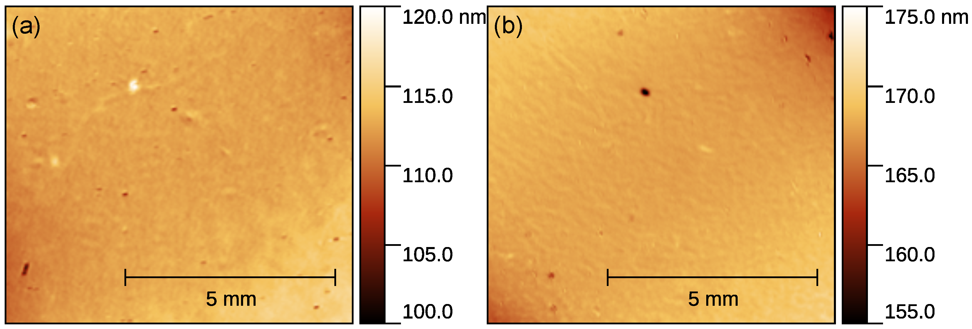
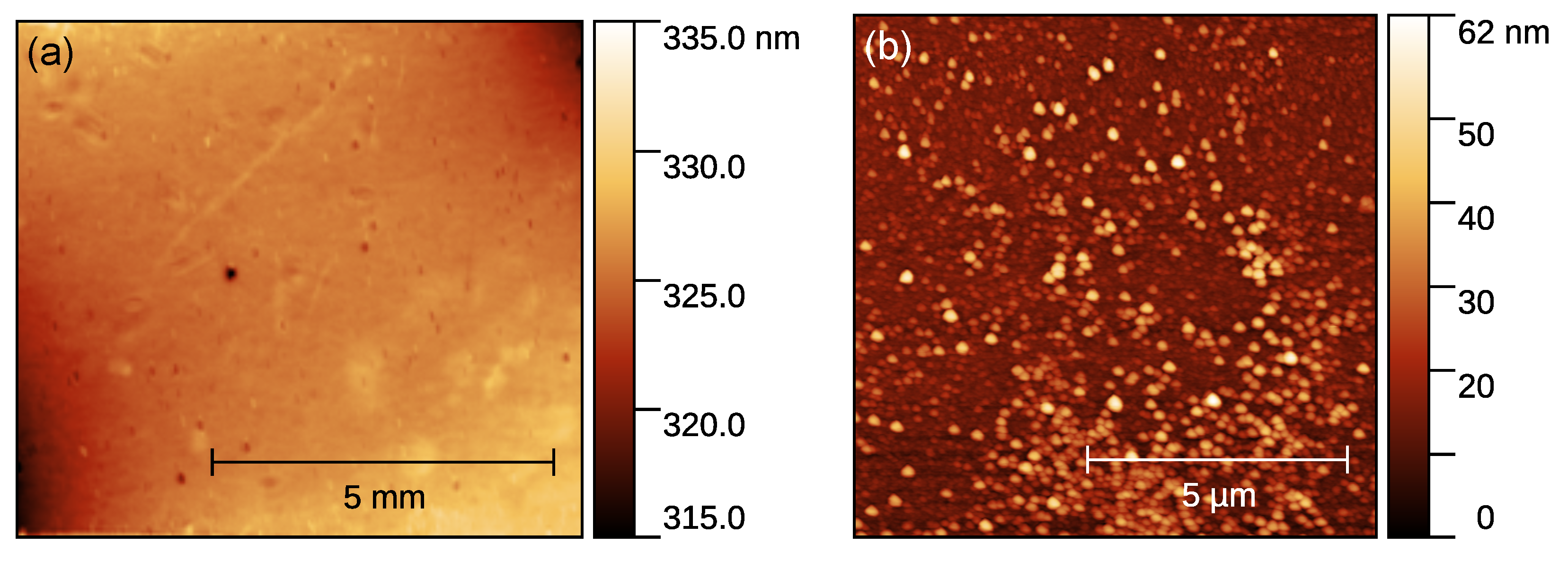
3.1. Sample Preparation

The thin films of non-stoichiometric silicon nitride were deposited onto one side of double-side polished silicon wafers. The deposition was performed by the reactive magnetron sputtering [39] of silicon target in argon-nitrogen atmosphere. The films were deposited using Vinci Technologies PVD 50S thin film deposition system. The pressure during the deposition was kept at constant value 10 2 mbar, and the flow rates of argon and nitrogen were Q Ar = 80 sccm and Q N 2 = 5 sccm. The power supply for the magnetron was set at 100 W. The films were deposited onto cold (unheated) substrates. Three samples with the same deposition conditions but different deposition times 30, 45 and 90 min were prepared.

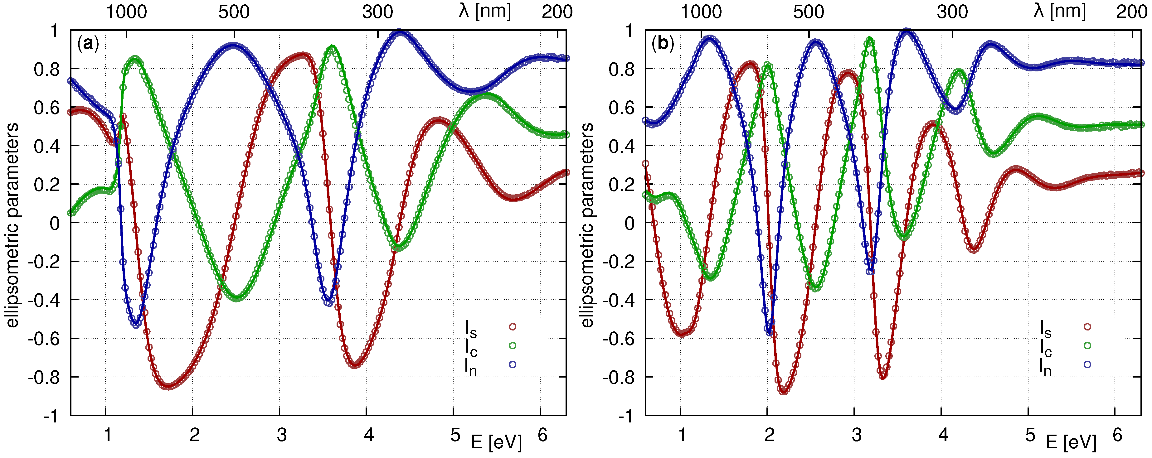
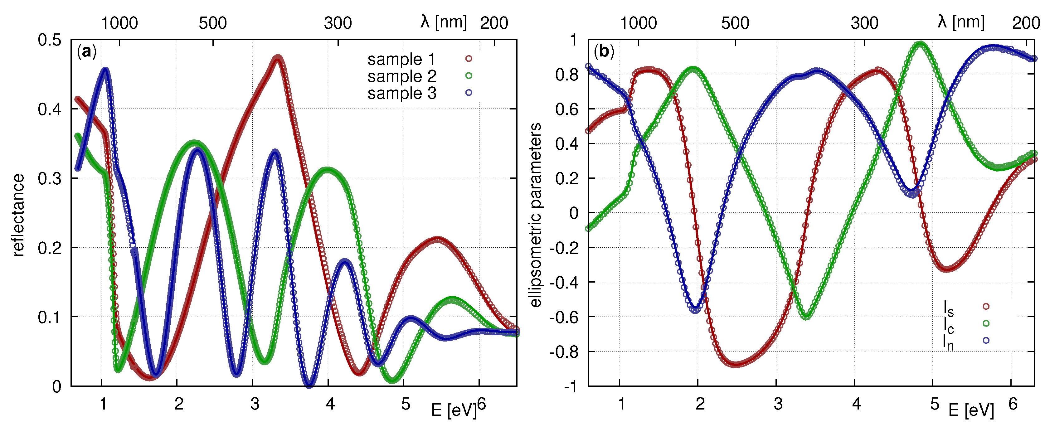
3.2. Experimental Data

The spectral dependencies of the ellipsometric parameters were measured using the Horiba Jobin Yvon UVISEL phase modulated ellipsometer (HORIBA Jobin Yvon, Irvine, CA, USA) for five incidence angles within the interval 55–75 and within the spectral range 0.6–6.3 eV (197–2066 nm). The spectral dependencies of the reflectance were measured by the Perkin Elmer Lambda 1050 spectrophotometer (Perkin Elmer, Waltham, MA, USA) at near normal incidence angle 6 within the spectral range 0.7–6.5 eV (190–1800 nm). The ISR data were measured at normal incidence within the spectral range 1.7–4.5 eV (275–700 nm), and the pixel size was 40 × 40 μ m. The Bruker Dimension Icon atomic force microscope (Bruker, Billerica, MA, USA) was used to investigate topography of surfaces of the samples. The X-ray diffraction curves have been measured on the PaNalytical X’Pert MRD diffractometer (Malvern PaNalytical, Malvern, UK), using standard X-ray tube (Cu, long-fine focus, 45 kV, 30 mA).

3.3. Data Processing

To interpret the experimental data, it was necessary to assume that the non-stoichiometric silicon nitride films are inhomogeneous and that they also exhibit uniaxial anisotropy. The inhomogeneity of the films was modeled by considering the profiles of the dispersion parameters given in Equation (39). Two values must be provided for each dispersion parameter, one specifying its value at the upper boundary of the film (i.e., for z = 0 ) and one specifying its value for z . Moreover, the number of dispersion parameters was further doubled due to the uniaxial anisotropy because a separate set of dispersion parameters must be used for the ordinary and extraordinary dielectric functions. The dielectric function given in Equation (31) is a function of eight dispersion parameters, therefore 4 × 8 parameters were used to describe the profile of the dielectric tensor. If all of these parameters were considered to be independent, the model would be overparameterized. Therefore, it was necessary to reduce the number of parameters sought in processing of the experimental data. It is reasonable to expect that the inhomogeneity of the film and the uniaxial anisotropy are relatively weak effects. Thus, it is possible to assume that some of the dispersion parameters do not exhibit profile (i.e., they have the same value at the upper boundary and for z ) and that some dispersion parameters have the same value for the ordinary and extraordinary dielectric functions. Even though the number of the parameters sought was reduced in this way, there were still enough degrees of freedom left to successfully interpret the measured experimental data.
The dispersion parameters used to describe the studied films could be separated into three groups. The four dispersion parameters E h , B ex , N ut and E u constituting the first group were assumed to be without a profile and, moreover, the same values were used for the ordinary and extraordinary dielectric functions. The second group consisting of E g , A ex and E ex represented dispersion parameters sought independently for the ordinary and the extraordinary dielectric functions and, furthermore, it was assumed that these parameters exhibit profiles. This means that four versions were considered for each of these parameters, two of them for the values of the ordinary and extraordinary dielectric functions at the upper boundary of the film and two for the values corresponding to the ordinary and extraordinary dielectric functions for z . The last group consisted of only one parameter, N vc , which specifies the total strength of valence to conduction band transitions. It was assumed that this parameter exhibits profile, thus its value was sought independently for the upper boundary of the film and for z . However, the same values were used for the ordinary and extraordinary dielectric functions. This is necessary to ensure the fulfillment of the condition in Equation (37), which ensures that the sum rule integral gives the same value for the ordinary and extraordinary dielectric functions (last condition in Equation (27)). The summary of the dispersion parameters describing the inhomogeneous film with uniaxial anisotropy is presented in Table 1.
The multi-sample method [40,41,42] was used to process the experimental data. In the multi-sample method, the experimental data measured on several samples by various techniques (reflectometry and ellipsometry) are processed simultaneously. In our case, the reflectometric and ellipsometric data measured on three samples were processed simultaneously. The samples were prepared under the same deposition conditions but with different deposition times, thus the thickness of the silicon nitride films was different for each film. All dispersion parameters with the exception of the parameters N vc were assumed to be the same for the silicon nitride films on all three samples. The values of the dispersion parameters N vc were sought independently for each sample in order to account for small variations in the optical constants of the individual films. This is indicated in the column “different for each sample” in Table 1. Since it was not possible to ensure that the reflectometric and ellipsometric data were measured on the same spots on the samples and the films may exhibit slight non-uniformity in thickness, two film thicknesses were sought for each sample. The first one was used in the processing of the reflectometric data and the other was used in the processing of the ellipsometric data. The values of the profile parameter w used in Equation (39) and the rms values of the heights used to describe the random roughness of the surfaces of the films were sought independently for each sample. By simultaneous processing of experimental data measured on samples with considerably different thicknesses but otherwise very similar properties, it was possible to decrease the correlation among the sought parameters.
The experimental data were processed using the newAD2 open-source software by the least squares method. The objective function was given as
S = i = 1 3 f i R NIR S i R NIR + i = 1 3 f i R UVV S i R UVV + i = 1 3 f i E S i E ,
where the index i distinguishes individual samples and S i R NIR , S i R UVV and S i E are the weighted sums of squares corresponding to the reflectometry in the near infrared region, reflectometry in the visible and ultraviolet region and ellipsometry measured on a given sample. The factors f i R NIR , f i R UVV and f i E are the weights for sums of squares of individual measurements. Their values were determined automatically by the algorithm that ensures the contribution to the objective function was approximately the same for each measurement. If these factors were not used, then measurements with large number of points or incorrectly estimated errors could overweigh contributions from the other measurements. This would create a situation in which the influence of some measurements on the sought parameters would be strong while the influence of the other measurements would be negligible.
The experimental data obtained using the imaging spectroscopic reflectometry were processed using the same structural and dispersion models as the reflectometric and ellipsometric data. The thickness of the films was sought independently for each pixel using the least squares method. The values of all the other structural and dispersion parameters were fixed in the values found in the processing of the reflectometric and ellipsometric data.

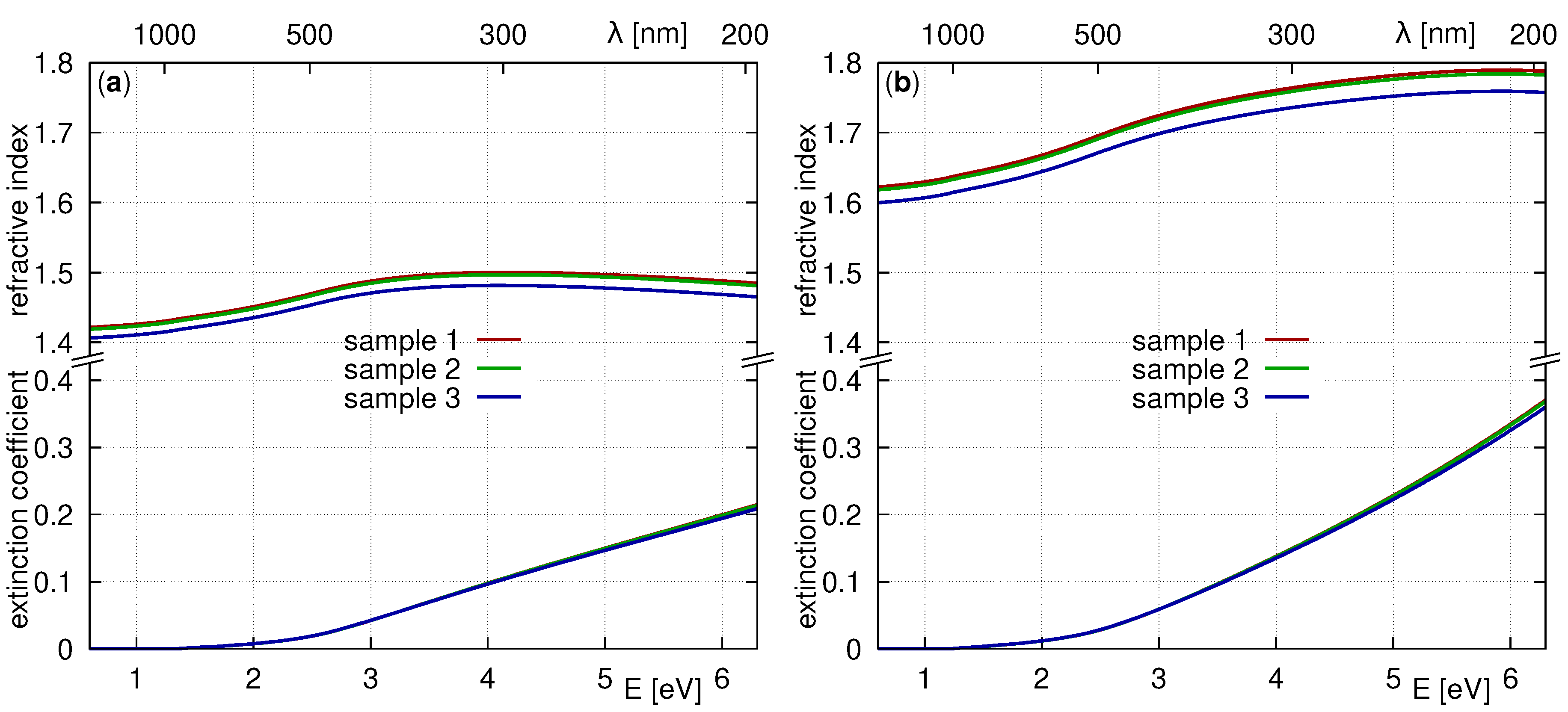
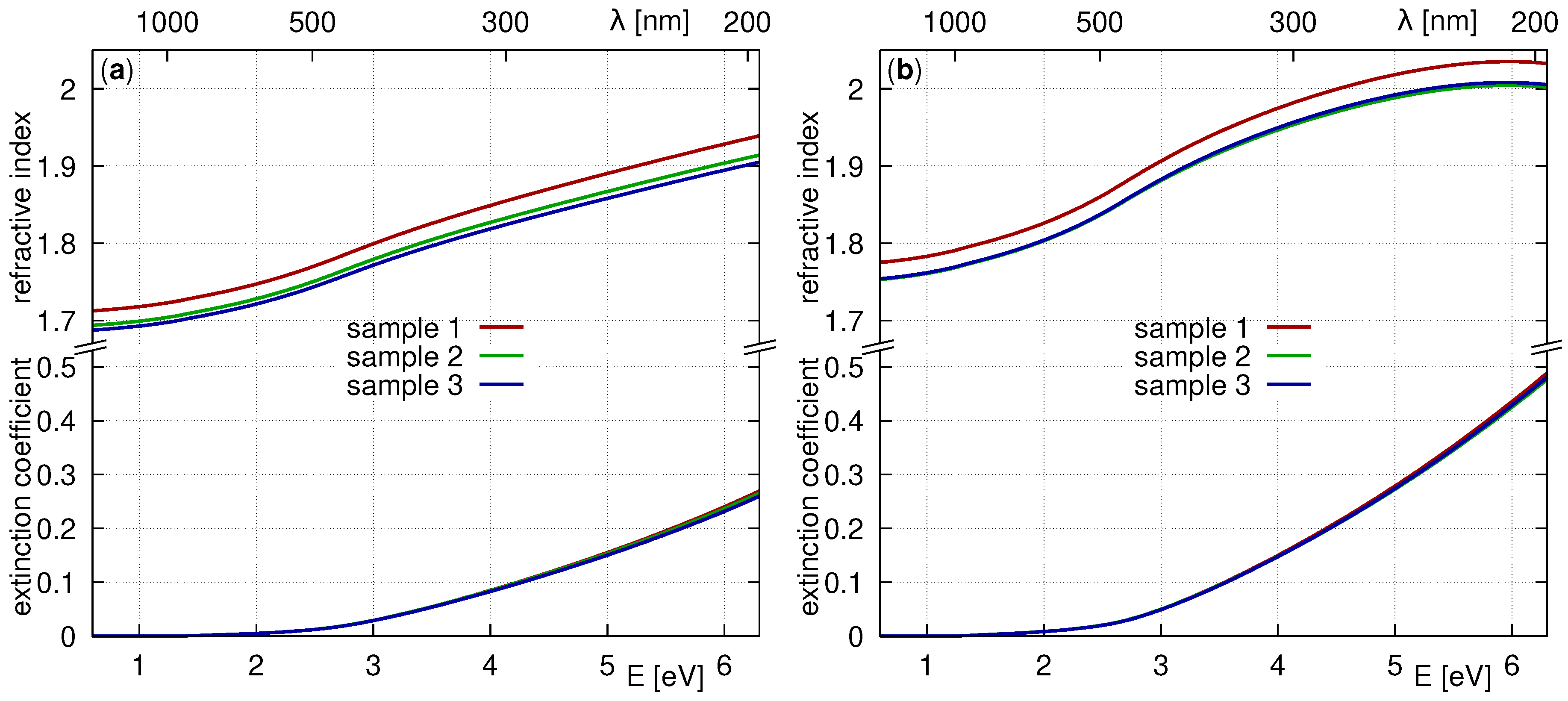
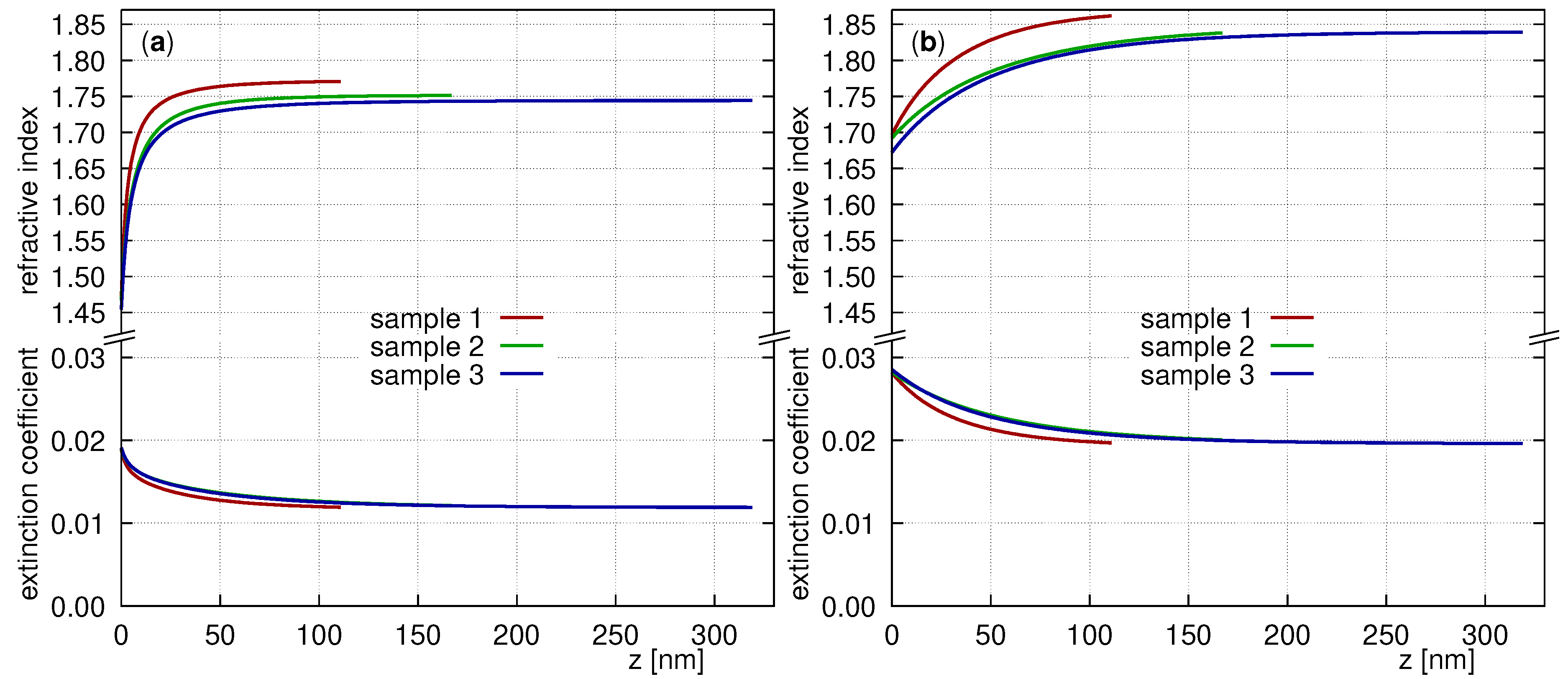
4. Results and Discussion

The results determined by the simultaneous processing of experimental data of all three samples are presented in Table 2. Thickness values corresponding to the ellipsometry and reflectometry for the individual samples are mutually very close, which means that the thickness non-uniformity of the samples is very small. The thickness values of individual samples increase approximately linearly with the deposition times. The rms values of the heights σ of the random roughness are also increasing with the deposition time.
The values of the dispersion parameters are presented in Table 3. This table is divided into three parts. In each part, the values of the dispersion parameters corresponding to groups introduced in Table 1 are listed. The spectral dependencies of the optical constants of the inhomogeneous films for the ordinary and the extraordinary waves at the upper and lower boundaries are presented in Figure 2 and Figure 3. Note that the complex refractive indices are defined as n ^ o = ε ^ o for the ordinary wave and as n ^ e = ε ^ e for the extraordinary wave. They could be written as n ^ o = n o + i k o and n ^ e = n e + i k e , where n o and n e are the real refractive indices and k o and k e are the extinction coefficients.
The profiles of the optical constants corresponding to the ordinary and extraordinary waves are displayed in Figure 4. In this figure, it is evident that the profiles of the inhomogeneous films on Samples 2 and 3 are very similar while the profile exhibited by Sample 1 is somewhat different from the other two samples. This is also visible in Figure 3 on the spectral dependencies of the optical constants at the lower boundary, which are almost the same for Samples 2 and 3 while the refractive indices of Sample 1 are little higher. Moreover, the values of the profile parameters w are almost the same for Samples 2 and 3 but the value determined for Sample 1 is lower than the values determined for the other two samples. However, we should note that the spectral dependencies of the optical constants at the upper boundary exhibit different behavior. The refractive indices corresponding to Samples 1 and 2 are almost the same while the refractive index corresponding to Sample 3 is little lower. Nevertheless, the differences between the optical constants at the upper and lower boundary are relatively small. This means that the inhomogeneity in the optical constants of all three samples exhibits practically the same behavior. The optical constants change in the vicinity of the upper boundary while the lower parts of the films are almost homogeneous. In Figure 2, Figure 3 and Figure 4, it is evident that the refractive indices are smaller at the upper boundaries and higher at the lower boundaries. This is probably connected with the technological process of creating the films.
We also tried to use a similar model with exponential profile in which the optical constants changed near the lower boundary and the upper parts of the films were almost homogeneous. However, this model could not correctly describe the experimental data.
In Section 2.3, the formulae derived within the SDT use the approximation that the optical constants in the range of roughness are constant. Figure 4 shows that the optical constants exhibit non-negligible changes within this range. Thus, the approach that we used to include the influence of the roughness on the optical quantities should be considered to be only a rough approximation. Since the roughness is slight (the rms values of the heights are small), the use of this rough approximation is permissible. This is also supported by the very good fits of the experimental data plotted in Figure 5 and Figure 6.
The thickness of the silicon single crystal substrate was determined using the micrometer screw gauge as 0.585 mm. The thicknesses of the native oxide layers on the back sides of the substrates were determined on the basis of the ellipsometric data measured on the back sides at angle of incidence 65 . The determined values were 3.09 nm for Sample 1, 2.74 nm for Sample 2 and 3.38 nm for Sample 3.
The maps of local thicknesses obtained by ISR are presented in Figure 7 and Figure 8. From these maps, it is clear that the certain non-uniformity in thickness occurs near the edges of the samples. In the central parts of the samples, the inhomogeneous films are practically uniform in thickness. Since the measurements were performed in these uniform parts, it was not necessary to include the thickness non-uniformity into our structural model.
The topography of the surface of Sample 3 obtained by AFM is introduced in Figure 8. The rms value of the heights determined from the AFM image is 7.50 ± 0.04 nm. This is in a relatively good agreement with the rms value of the heights determined by means of the optical method 6.3 ± 0.2 nm.

5. Conclusions

In this study, the optical characterization of the non-stoichiometric silicon nitride films prepared by the reactive magnetron sputtering was performed. To interpret the experimental data, it was necessary to assume that the characterized films exhibit several defects. The original model combining these defects had to be developed. These defects are the inhomogeneity in the optical constants, uniaxial anisotropy with optical axis perpendicular to the boundaries and the roughness of the upper boundaries of the films. The inhomogeneity is represented by profiles of the optical constants across the films.
The simultaneous inclusion of inhomogeneity and anisotropy was achieved using the approximation in which the inhomogeneous layer was approximated by a multi-layer system consisting of large number of thin homogeneous layers. Since the inhomogeneous film was anisotropic, the individual layers in this multi-layer system were also assumed to be anisotropic. The optical quantities of the multi-layer system were calculated using the Yeh matrix formalism. The random roughness of the upper boundaries of the studied films was included using the SDT under the assumption that the optical constants exhibit only small changes in the range of this roughness.
The optical characterization was performed on the basis of the ellipsometric and reflectometric data measured within the spectral range 0.6–6.3 eV. The inclusion of all defects required a model depending on a large number of parameters. To reduce the correlation among the parameters sought within the data processing, the multi-sample method was utilized. The experimental data measured on three samples prepared with different deposition times (i.e., differing in thickness) were processed simultaneously.
It was found that the films exhibited profiles of the optical constants, which can be described using the exponential function so that the pronounced changes of the optical constants occur in the region near the upper boundary. Within the substantial part of the film, the optical constants were practically constant. The evident uniaxial anisotropy with the optical axis perpendicular to the boundaries corresponded to different values of the optical constants for the ordinary and extraordinary waves. Furthermore, the rms values of the heights of the roughness were found in the range of nanometers for all three films.
The ISR was utilized to investigate the thickness non-uniformity of the films. It was found that the films are uniform in thickness along the substantial parts of their area; slight thickness non-uniformity was observed only in the regions near the edges.

Author Contributions

Conceptualization, I.O. and M.O.; Methodology, J.V. and I.O.; Software, J.V. and D.F.; and Investigation, J.V., D.F., Š.Š., M.Č., V.Š., P.V. and J.Ž.

Funding

This work was supported by the project LO1411 (NPU I) funded by Ministry of Education, Youth and sports of the Czech Republic and the project FSI-S-17–4506 funded by Brno University of Technology.

Acknowledgments

We would like to thank V. Holý from the Department of Condensed Matter Physics at the Faculty of Science, Masaryk University for X-ray measurements and analysis of the samples and to P. Klapetek M. Valtr from the Czech Metrology Institute for preparing and measuring the AFM images of the samples.

Conflicts of Interest

The authors declare no conflict of interest. The funders had no role in the design of the study; in the collection, analyses, or interpretation of data; in the writing of the manuscript, or in the decision to publish the results.

References

  1. Ghosh, H.; Mitra, S.; Saha, H.; Datta, S.K.; Banerjee, C. Argon plasma treatment of silicon nitride (SiN) for improved antireflection coating on c-Si solar cells. Mater. Sci. Eng. B Adv. 2017, 215, 29–36. [Google Scholar] [CrossRef]
  2. Kishore, R.; Singh, S.; Das, B. PECVD grown silicon nitride AR coatings on polycrystalline silicon solar cells. Sol. Energy Mater. Sol. Cells 1992, 26, 27–35. [Google Scholar] [CrossRef]
  3. Cai, L.; Rohatgi, A.; Yang, D.; El-Sayed, M.A. Effects of rapid thermal anneal on refractive index and hydrogen content of plasma-enhanced chemical vapor deposited silicon nitride films. J. Appl. Phys. 1996, 80, 5384–5388. [Google Scholar] [CrossRef]
  4. Doshi, P.; Jellison, G.E.; Rohatgi, A. Characterization and optimization of absorbing plasma-enhanced chemical vapor deposited antireflection coatings for silicon photovoltaics. Appl. Opt. 1997, 36, 7826–7837. [Google Scholar] [CrossRef] [PubMed]
  5. Misiakos, I.; Tsoi, E.; Halmagean, E.; Kakabakos, S. Monolithic integration of light emitting diodes, detectors and optical fibers on a silicon wafer: A CMOS compatible optical sensor. In Proceedings of the International Electron Devices Meeting 1998, San Francisco, CA, USA, 6–9 Decemeber 1998; pp. 25–28. [Google Scholar]
  6. Adams, A. Dielectric and polysilicon film deposition. In VLSI technology; Sze, S.H., Ed.; McGraw-Hill Higher Education: New York, NY, USA, 1988. [Google Scholar]
  7. Vernhes, R.; Zabeida, O.; Klemberg-Sapieha, J.E.; Martinu, L. Single-material inhomogeneous optical filters based on microstructural gradients in plasma-deposited silicon nitride. Appl. Opt. 2004, 43, 97–103. [Google Scholar] [CrossRef] [PubMed]
  8. Huang, S.; Arai, K.; Usami, K.; Oda, S. Toward long-term retention-time single-electron-memory devices based on nitrided nanocrystalline silicon dots. IEEE Trans. Nanotechnol. 2004, 3, 210–214. [Google Scholar] [CrossRef]
  9. Yang, M.S.; Cho, K.S.; Jhe, J.H.; Seo, S.Y.; Shin, J.H.; Kim, K.J.; Moon, D.W. Effect of nitride passivation on the visible photoluminescence from Si-nanocrystals. Appl. Phys. Lett. 2004, 85, 3408–3410. [Google Scholar] [CrossRef] [Green Version]
  10. Arora, W.J.; Nichol, A.J.; Smith, H.I.; Barbastathis, G. Membrane folding to achieve three-dimensional nanostructures: Nanopatterned silicon nitride folded with stressed chromium hinges. Appl. Phys. Lett. 2006, 88, 053108. [Google Scholar] [CrossRef]
  11. Debieu, O.; Nalini, R.P.; Cardin, J.; Portier, X.; Perrière, J.; Gourbilleau, F. Structural and optical characterization of pure Si-rich nitride thin films. Nanoscale Res. Lett. 2013, 8, 31. [Google Scholar] [CrossRef]
  12. Kim, J.H.; Chung, K.W. Microstructure and properties of silicon nitride thin films deposited by reactive bias magnetron sputtering. J. Appl. Phys. 1998, 83, 5831–5839. [Google Scholar] [CrossRef]
  13. Asinovsky, L.; Shen, F.; Yamaguchi, T. Characterization of the optical properties of PECVD SiNx films using ellipsometry and reflectometry. Thin Solid Films 1998, 313–314, 198–204. [Google Scholar] [CrossRef]
  14. Jellison, G.E., Jr.; Modine, F.A.; Doshi, P.; Rohatgi, A. Spectroscopic ellipsometry characterization of thin-film silicon nitride. Thin Solid Films 1998, 313–314, 193–197. [Google Scholar] [CrossRef]
  15. Franta, D.; Ohlídal, I. Ellipsometric parameters and reflectances of thin films with slightly rough boundaries. J. Mod. Opt. 1998, 45, 903–934. [Google Scholar] [CrossRef]
  16. Ohlídal, I.; Vohánka, J.; Čermák, M.; Franta, D. Optical characterization of randomly microrough surfaces covered with very thin overlayers using effective medium approximation and Rayleigh–Rice theory. Appl. Surf. Sci. 2017, 419, 942–956. [Google Scholar] [CrossRef]
  17. Ohlídal, I.; Vohánka, J.; Mistrík, J.; Čermák, M.; Franta, D. Different theoretical approaches at optical characterization of randomly rough silicon surfaces covered with native oxide layers. Surf. Interface Anal. 2018, 50, 1230–1233. [Google Scholar] [CrossRef]
  18. Ohlídal, I.; Navrátil, K.; Lukeš, F. Reflection of light by a system of nonabsorbing isotropic film–Nonabsorbing isotropic substrate with randomly rough boundaries. J. Opt. Soc. Am. 1971, 61, 1630–1639. [Google Scholar] [CrossRef]
  19. Ohlídal, I.; Lukeš, F. Ellipsometric parameters of rough surfaces and of a system substrate-thin film with rough boundaries. Opt. Acta 1972, 19, 817–843. [Google Scholar] [CrossRef]
  20. Ohlídal, I. Approximate formulas for the reflectances, transmittances, and scattering losses of nonabsorbing multilayers systems with randomly rough boundaries. J. Opt. Soc. Am. A 1993, 10, 158–170. [Google Scholar] [CrossRef]
  21. Ohlídal, I.; Navrátil, K.; Ohlídal, M. Scattering of light from multilayer systems with rough boundaries. In Progress in Optics; Wolf, E., Ed.; Elsevier: Amsterdam, The Netherlands, 1995; Volume 34, pp. 249–331. [Google Scholar]
  22. Ohlídal, I.; Franta, D.; Nečas, D. Improved combination of scalar diffraction theory and Rayleigh-Rice theory and its application to spectroscopic ellipsometry of randomly rough surfaces. Thin Solid Films 2014, 571, 695–700. [Google Scholar] [CrossRef]
  23. Ohlídal, I.; Vižďa, F.; Ohlídal, M. Optical analysis by means of spectroscopic reflectometry of single and double layers with correlated randomly rough boundaries. Opt. Eng. 1995, 34, 1761–1768. [Google Scholar] [CrossRef]
  24. Yeh, P. Optics of anisotropic layered media: A new 4 × 4 matrix algebra. Surf. Sci. 1980, 96, 41–53. [Google Scholar] [CrossRef]
  25. Knittl, Z. Optics of Thin Films; Wiley: London, UK, 1976. [Google Scholar]
  26. Ohlídal, I.; Vohánka, J.; Čermák, M.; Franta, D. Ellipsometry of layered systems. In Optical Characterization of Thin Solid Films; Stenzel, O., Ohlídal, M., Eds.; Springer International Publishing: Cham, Switzerland, 2018; pp. 233–267. [Google Scholar]
  27. Vohánka, J.; Ohlídal, I.; Ženíšek, J.; Vašina, P.; Čermák, M.; Franta, D. Use of the Richardson extrapolation in optics of inhomogeneous layers: Application to optical characterization. Surf. Interface Anal. 2018, 50, 757–765. [Google Scholar] [CrossRef]
  28. Franta, D.; Dubroka, A.; Wang, C.; Giglia, A.; Vohánka, J.; Franta, P.; Ohlídal, I. Temperature-dependent dispersion model of float zone crystalline silicon. Appl. Surf. Sci. 2017, 421, 405–419. [Google Scholar] [CrossRef]
  29. Franta, D.; Nečas, D.; Ohlídal, I.; Giglia, A. Optical characterization of SiO2 thin films using universal dispersion model over wide spectral range. In Proceedings of the SPIE Photonics Europe, Brussels, Belgium, 3–7 April 2016; Volume 9890, p. 989014. [Google Scholar]
  30. Franta, D.; Nečas, D.; Ohlídal, I. Universal dispersion model for characterization of optical thin films over wide spectral range: Application to hafnia. Appl. Opt. 2015, 54, 9108–9119. [Google Scholar] [CrossRef] [PubMed]
  31. Franta, D.; Vohánka, J.; Čermák, M. Universal dispersion model for characterisation of thin films over wide spectral range. In Optical Characterization of Thin Solid Films; Stenzel, O., Ohlídal, M., Eds.; Springer International Publishing: Cham, Switzerland, 2018; pp. 31–82. [Google Scholar]
  32. Franta, D.; Nečas, D.; Zajíčková, L. Application of Thomas–Reiche–Kuhn sum rule to construction of advanced dispersion models. Thin Solid Films 2013, 534, 432–441. [Google Scholar] [CrossRef]
  33. Franta, D.; Nečas, D.; Zajíčková, L.; Ohlídal, I.; Stuchlík, J.; Chvostová, D. Application of sum rule to the dispersion model of hydrogenated amorphous silicon. Thin Solid Films 2013, 539, 233–244. [Google Scholar] [CrossRef]
  34. Ohlídal, M.; Vodák, J.; Nečas, D. Optical characterization of thin films by means of imaging spectroscopic reflectometry. In Optical Characterization of Thin Solid Films; Stenzel, O., Ohlídal, M., Eds.; Springer International Publishing: Cham, Switzerland, 2018; pp. 107–141. [Google Scholar]
  35. Ohlídal, I.; Ohlídal, M.; Nečas, D.; Franta, D.; Buršíková, V. Optical characterisation of SiOxCyHz thin films non-uniform in thickness using spectroscopic ellipsometry, spectroscopic reflectometry and spectroscopic imaging reflectometry. Thin Solid Films 2011, 519, 2874–2876. [Google Scholar] [CrossRef]
  36. Nečas, D.; Ohlídal, I.; Franta, D.; Ohlídal, M.; Čudek, V.; Vodák, J. Measurement of thickness distribution, optical constants, and roughness parameters of rough nonuniform ZnSe thin films. Appl. Opt. 2014, 53, 5606–5614. [Google Scholar] [CrossRef]
  37. Nečas, D.; Čudek, V.; Vodák, J.; Ohlídal, M.; Klapetek, P.; Benedikt, J.; Rügner, K.; Zajíčková, L. Mapping of properties of thin plasma jet films using imaging spectroscopic reflectometry. Meas. Sci. Technol. 2014, 25, 115201. [Google Scholar] [CrossRef]
  38. Nečas, D.; Ohlídal, I.; Franta, D.; Čudek, V.; Ohlídal, M.; Vodák, J.; Sládková, L.; Zajíčková, L.; Eliáš, M.; Vižďa, F. Assessment of non-uniform thin films using spectroscopic ellipsometry and imaging spectroscopic reflectometry. Thin Solid Films 2014, 571, 573–578. [Google Scholar] [CrossRef]
  39. Berg, S.; Nyberg, T. Fundamental understanding and modeling of reactive sputtering processes. Thin Solid Films 2005, 476, 215–230. [Google Scholar] [CrossRef]
  40. Franta, D.; Ohlídal, I.; Klapetek, P. Analysis of slightly rough thin films by optical methods and AFM. Mikrochim. Acta 2000, 132, 443–447. [Google Scholar] [CrossRef]
  41. Franta, D.; Ohlídal, I. Analysis of thin films by optical multi-sample methods. Acta Phys. Slov. 2000, 50, 411–421. [Google Scholar]
  42. Franta, D.; Zajíčková, L.; Ohlídal, I.; Janča, J.; Veltruská, K. Optical characterization of diamond like carbon films using multi-sample modification of variable angle spectroscopic ellipsometry. Diam. Relat. Mater. 2002, 11, 105–117. [Google Scholar] [CrossRef]
Figure 1. Schematic diagram of the division of the inhomogeneous film into thin homogeneous slices.
Coatings 09 00416 g001
Figure 2. Spectral dependencies of the optical constants of the inhomogeneous films at the upper boundary for: ordinary wave (a); and extraordinary wave (b).
Coatings 09 00416 g002
Figure 3. Spectral dependencies of the optical constants of the inhomogeneous films at the lower boundary for: ordinary wave (a); and extraordinary wave (b).
Coatings 09 00416 g003
Figure 4. The profiles of the optical constants of the inhomogeneous films of refractive index for the selected photon energy E = 2.5 eV (496 nm) for: ordinary wave (a); and extraordinary wave (b). The coordinate z is directed such that it corresponds to the depth inside the inhomogeneous films (i.e., the distance form the upper boundary).
Coatings 09 00416 g004
Figure 5. Spectral dependencies of the associated ellipsometric parameters of Sample 2 (a) and Sample 3 (b) at incidence angle 70 : points denote the measured values, curves denote the theoretical values.
Coatings 09 00416 g005
Figure 6. Spectral dependencies of reflectance of all three samples (a) and the associated ellipsometric parameters of Sample 1 at incidence angle 70 (b): points denote the measured values, curves denote the theoretical values.
Coatings 09 00416 g006
Figure 7. The map of the local thicknesses determined by ISR for: Sample 1 (a); and Sample 2 (b).
Coatings 09 00416 g007
Figure 8. The map of the local thicknesses determined by ISR for Sample 3 (a); and topography of the upper boundary of Sample 3 measured by AFM (b).
Coatings 09 00416 g008
Table 1. Summary of dispersion parameters.
ParametersExhibit ProfileDifferent for ε ^ o and ε ^ e Different for Each Sample
N vc yesnoyes
E g , A ex , E ex yesyesno
E h , N ut , E u , B ex nonono
Table 2. The values of the structural parameters.
Parameter Sample 1Sample 2Sample 3
deposition timet[min]304590
thickness ellipsometry d e [nm] 111.21 ± 0.05 167.10 ± 0.08 323.9 ± 0.1
thickness reflectance d r [nm] 112.12 ± 0.06 167.91 ± 0.07 320.80 ± 0.09
roughness (rms) σ [nm] 3.0 ± 0.2 4.6 ± 0.2 6.3 ± 0.2
profile parameterw[nm] 39.3 ± 1.8 65.6 ± 2.8 57.6 ± 2.6
Table 3. The values of the dispersion parameters.
Parameter
E h [eV] 70.0 ± 1.6
B ex [eV] 3.90 ± 0.03
N ut [eV 2 ] 37.8 ± 2.6
E u [eV] 0.405 ± 0.002
Parameters without profile which are identical for the ordinary and extraordinary dielectric functions
Parameter Upper Boundary z
N vc [eV 2 ]Sample 1 401.6 ± 3.2 453.7 ± 3.4
Sample 2 398.0 ± 3.5 437.1 ± 3.3
Sample 3 381.6 ± 2.9 430.8 ± 3.2
Parameters with profile which are identical for the ordinary and extraordinary dielectric functions
Upper Boundary z
Parameter OrdinaryExtraordinaryOrdinaryExtraordinary
E g [eV] 2.65 ± 0.03 2.43 ± 0.0 2.77 ± 0.03 2.55 ± 0.02
A ex 0.21 ± 0.03 1.1 ± 0.1 11.8 ± 1.1 2.4 ± 0.1
E ex [eV] 10.31 ± 0.05 9.15 ± 0.07 11.20 ± 0.02 8.65 ± 0.05
Parameters with profile which are different for the ordinary and extraordinary dielectric functions

