Article

Growth and Correlation of the Physical and Structural Properties of Hexagonal Nanocrystalline Nickel Oxide Thin Films with Film Thickness

by
Ahmed H. Hammad
1,2,*,
Mohamed Sh. Abdel-wahab
1,3,
Sajith Vattamkandathil
1 and
Akhalakur Rahman Ansari
1
1
Center of Nanotechnology, King Abdulaziz University, Jeddah 21589, Saudi Arabia
2
Electron Microscope and Thin Films Department, Physics Division, National Research Centre, Dokki, Giza 12622, Egypt
3
Materials Science and Nanotechnology Department, Faculty of Postgraduate Studies for Advanced Sciences, Beni-Suef University, Beni-Suef 62521, Egypt
*
Author to whom correspondence should be addressed.
Coatings 2019, 9(10), 615; https://doi.org/10.3390/coatings9100615
Submission received: 21 July 2019 / Revised: 20 September 2019 / Accepted: 24 September 2019 / Published: 26 September 2019

Abstract

:
This study investigated nonstoichiometric nickel oxide thin films prepared via the DC-sputtering technique at different film thicknesses. The prepared films were characterized by a surface profiler for thickness measurement, X-ray diffraction (XRD) for film nature, atomic force microscopy (AFM) for film morphology and roughness, UV-visible-near infrared (UV-vis.-NIR) spectroscopy for optical transmittance spectra of the films, and the photoluminescence (PL) spectra of the prepared films were obtained. The measured film thickness increased from 150 to 503 nm as the deposition time increased. XRD detected the trigonal crystal system of NiO0.96. The crystallite sizes were mainly grown through (101) and (110) characteristic planes. NiO0.96 films have a spherical particle shape and their sizes decreases as the film thickness increased. The optical band gap values decrease from 3.817 to 3.663 eV when the film thickness increases. The refractive index was estimated from the Moss relation, while the high-frequency dielectric constant and the static dielectric constant were deduced from the empirical Adachi formula. The photoluminescence behavior of the studied films confirmed the photogeneration of an electron-hole in nickel and oxygen vacancies. Hence, this study confirms the presence of nickel oxide lattice in the hexagonal structure containing the defects originated from the nickel vacancies or the excess of oxygen.

1. Introduction

Three-dimensional transition metal oxide materials such as nickel oxide are mostly antiferromagnetic materials as a result of their partially filled 3d orbitals [1,2]. The magnetic moment of Ni2+ ions is ordered below the Néel point at 523 K, in which the spins are parallel through the (111) plane and antiparallel between the adjacent (111) plane [2]. Nickel oxide has different crystalline phases, such as the cubic phase (NiO) and the hexagonal phase (Ni2O3 and NiOx). However, nickel oxide crystals are predominately deficient due to the excess of oxygen atoms and the deficiency in the nickel structure. This causes nickel oxide crystals non-stoichiometries to show p-type semiconductor behavior [3,4]. Passerini and Scrosati [5] investigated non-stoichiometric nickel oxide thin films prepared by the DC-sputtering technique. They found that these films could be used as intercalation electrodes, and hence could be applied to the improvement of electrochromic displays [5]. The supercapacitor trend was affected through the formation of the non-stoichiometric layer of nickel oxide thin films by the RF-sputtering process [6]. The specific capacitance is strongly dependent on the nickel states in such films. Manceriu et al. [7] presented a method for the determination of sub-stoichiometric nickel oxide (Ni1−xO) and the effect of subsequent heat treatment. They suggested that increasing the Ni3+ state gives a deep brownish color and increases the film crystallinity. They also confirmed the non-stoichiometric ratio between the oxygen and nickel ions. Moreover, Kwon et al. [8] observed the phase of Ni2O3, along with the NiO phase. They suggested that the Ni2O3 phase was assembled by Ni vacancies in NiO films, which confirms non-stoichiometry in nickel oxide materials. Another observation of the hexagonal phase of nickel oxide was done by Zhu et al. [9], who observed a hexagonal side length of nanocrystals of nickel oxide, which was confirmed by high-resolution transmission electron microscopy (HRTEM). Recently, Hammad et al. [10] studied the behavior of non-stoichiometry nickel oxide prepared at various experimental oxygen gas rates, from 10 to 50 SCCM. They observed that the crystallites were mainly grown through the (101) and (012) planes for films prepared at a flow oxygen rate of 10 and 20 SCCM, while the crystallites were predominantly grown on the (101) plane at oxygen flow rates of 30, 40, and 50 SCCM. The increasing values in the energy gap are associated with the flow gas of oxygen from 3.74 eV/10 SCCM to 3.8 eV/50 SCCM.
Several preparation techniques are used to form nickel oxide films on glass substrate or indium doped tin oxide glass substrate such as sol-gel [11,12,13], chemical bath deposition [14,15,16], electron beam evaporation [17,18], and sputtering [19,20,21,22], among other things.
It is believed that distinct control in the preparation parameters gives good quality films that can be applied in different technological applications, such as photovoltaics [15], electrochromic devices [17], and supercapacitor electrochemical response [9], among others.
Based on the previous investigation by Hammad et al. [10], the created films were favorable in terms of the nonstoichiometric ratio between nickel and oxygen atoms. Hence, this research paper is an extension to previous reported work [10] aiming to study and investigate the correlation between the structure, morphology, and the optical properties of the deposited films at different higher thicknesses (more than 141 nm) in order to observe the growth mechanism of such materials at a fixed oxygen flow rate of 10 SCCM. The present research includes several techniques for characterization, including XRD, AFM, optical and photoluminescence characteristics.

2. Materials and Methods

Before depositing thin films on both the normal glass substrate and silicon wafer, they were washed in boiled distilled water. Then the substrates were transferred to an ultrasonic bath filled with a mixture of distilled water/ethanol for 1 h. Finally, they were dried by nitrogen gas at normal room temperature.
The sputtering technique (DC-sputtering, Syskey Technologies, Hsinch County, Taiwan) is used to deposit nickel oxide material on the glass substrates/silicon wafer by oxidation of the nickel target with a dimension of 3 × 0.6 inch at a power of 200 W at a constant oxygen flow rate of 10 SCCM and a flow of high-purity gas of argon (99.99%) at 20 SCCM on the substrate. The films are synthesized at an operating pressure of 5 mTorr and a substrate cycle of 15 rpm, and the Ni base targets to the substrate distance are fixed at 140 mm. Different thicknesses of nickel oxide films can be achieved at different deposition times of 1200, 1800, 2100, and 2400 s, as measured by a surface profiler, type Dektak XT, Bruker, Karlsruhe, Germany. Their values are presented in Table 1.
The film nature was detected using an X-ray diffraction device (type Ultima-IV; Rigaku, Tokyo, Japan) worked at 40 kV/40 mA with Cu kα radiation (λ = 0.154056 nm) in the angle range 20–80°. The surface film structure was investigated via atomic force microscopy type Omicron-UHV-VT-AFM XA through a contact mode under ultra-high vacuum conditions. The estimation of the grain size and the roughness were obtained by software described in detail in a previous article [10]. Optical transmittance was recorded via the spectrometer Perkin Elmer Lambda 750, Massachusetts, USA in the photon wavelength 190–2500 nm with a resolution of 1 nm. Photoluminescence (PL) RF-5301PC spectrofluorophotometer SHIMADZU, Kyoto, Japan was measured for investigation of the films’ luminescence at an excitation wavelength of 325 nm and at room temperature.

3. Results and Discussion

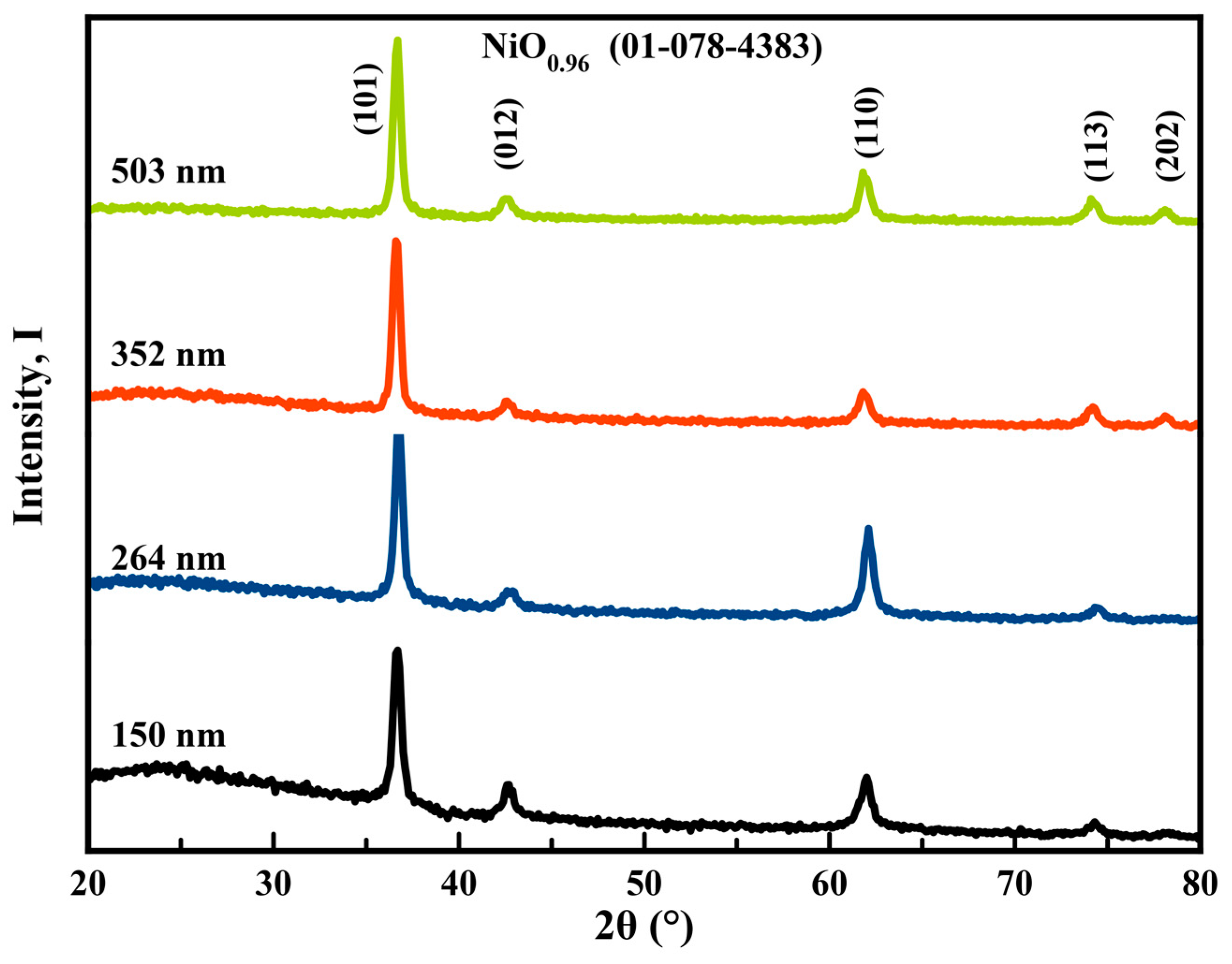
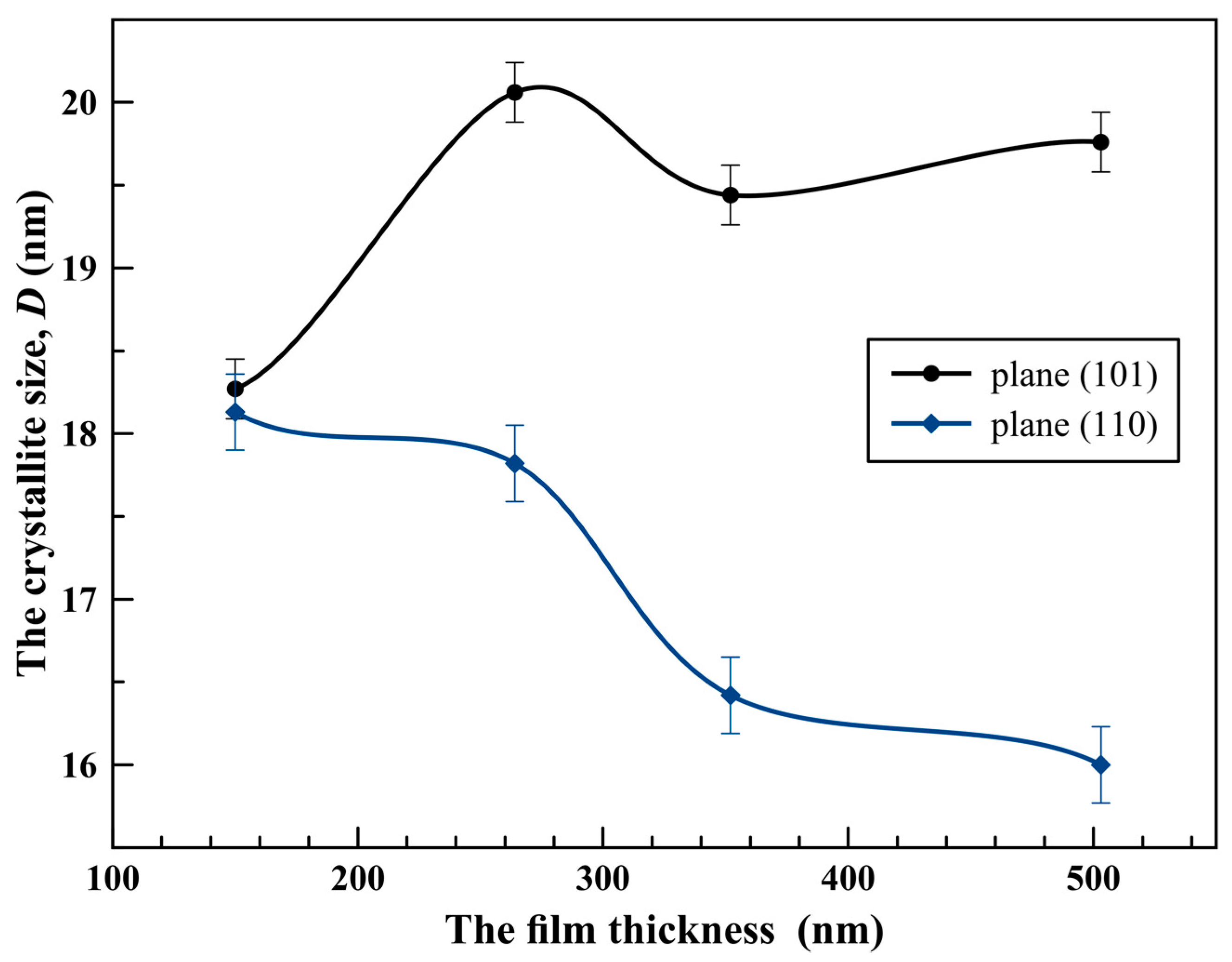
3.1. X-Ray Diffraction Analysis

The prepared samples showed the formation of a trigonal crystal system NiO0.96 of the card number (01-078-4383). The trigonal crystal system is in the hexagonal crystal family. Figure 1 represents the XRD patterns for different thicknesses of nickel oxide thin films. The characteristic planes are also included in the XRD chart. Five planes characterize the hexagonal structure of NiO0.96 films; (101) plane at 2θ~36.7°, (012) at 2θ~42.7°, (110) at 2θ~62.1°, (113) at 2θ~74.1°, and (202) at 2θ~78.1°. Indeed, plane (101) is the major plane in all samples due to the higher intensity than other planes. Additionally, plane (110) is next to plane (101) in intensity, instead of plane (012) for the prepared films at different oxygen flow rates as discussed previously [10]. Plane (110) was observed to become broader and the intensity was reduced as the deposition time increased.
The average crystallite size (D) of the crystals is determined from the Scherrer formula [23] for (101) and (110) planes, as follows:
D = 0.89 λ / β cos θ
where β is the full width at half maximum of the peak, and θ is the diffraction angle. The size grew through plane (101) (as seen in Figure 2) from 18.27 to 19.76 nm as the film thickness varied from 150 to 503 nm, while the crystallite size decreased slowly through plane (110).
XRD confirmed the nonstoichiometric ratio in the nickel oxide lattice. The crystallites were largely grown on planes (101) and (110). Therefore, under the present experimental condition of sputtered nickel oxide films, the crystallites preferred to grow on plane (101). The texture coefficient Tc(hkl) examined the preferred growth/orientation according to the following equation [24,25]:
T c ( hkl ) = I ( hkl ) / I o ( hkl ) ( 1 / N ) N ( I ( hkl ) / I o ( hkl ) )
where I(hkl) represents the experimentally measured intensity, Io(hkl) is the relative incident intensity given from the standard XRD card, and N denotes the diffraction peak numbers. Table 1 shows the texture coefficient values and the calculated crystallite size obtained from the XRD chart. The texture coefficient of (101) is higher than (110), which confirms the assumption of crystallite growth along (101). However, the texture coefficient values decreased when the film thickness increased, while the texture coefficient values for plane (110) increased when the thickness increased (except the nickel oxide sample with a thickness of 503 nm).

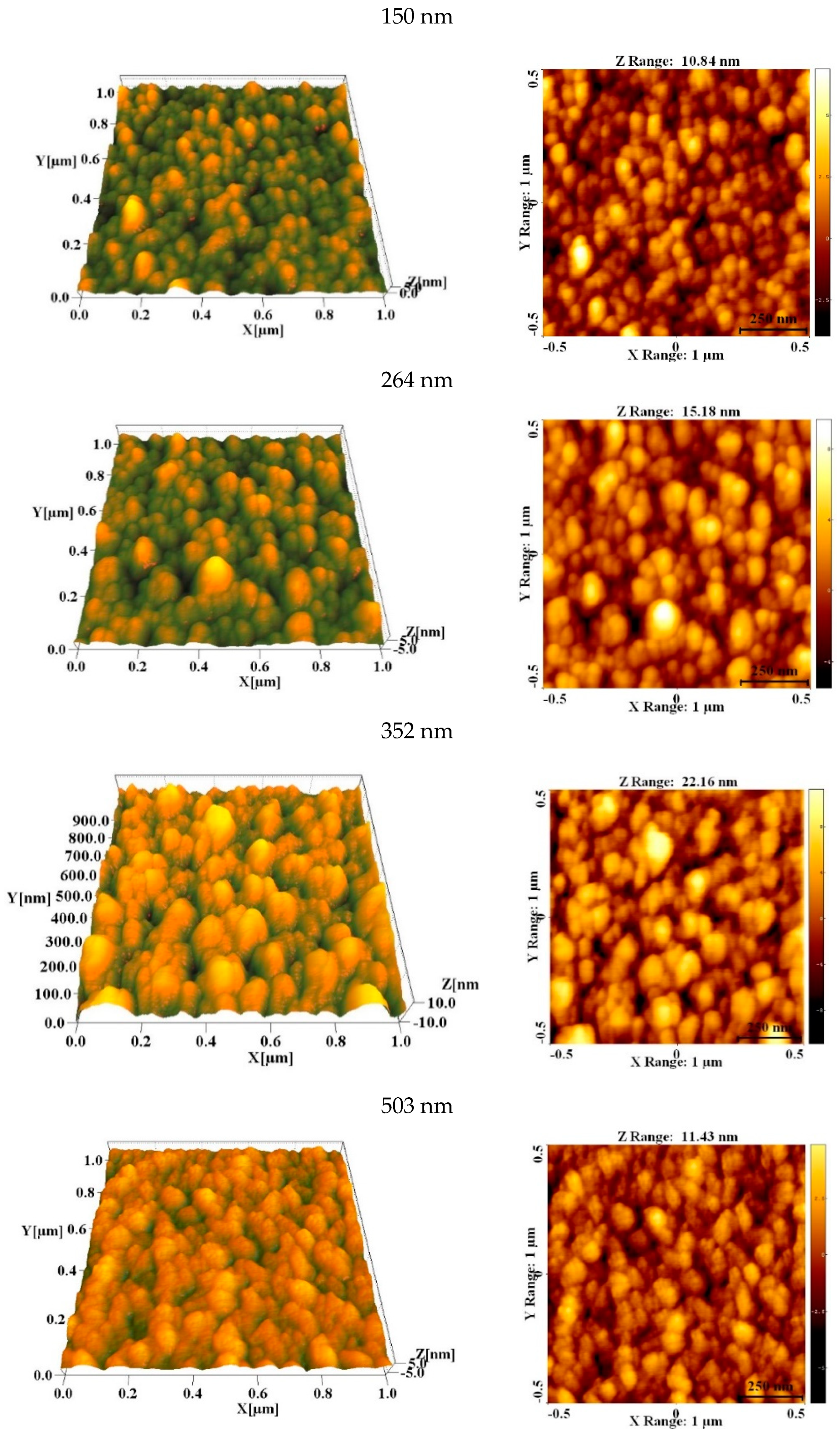
3.2. Surface Morphology Investigation

All samples have a spherical shape, as seen in Figure 3. Increasing the film thickness or the deposition time causes the grains to accumulate on the silicon wafer substrates. The grain size decreases from 48.85 to 30.68 nm as the film thickness increases. Nickel oxide films with a thickness of 503 nm show the highest surface roughness relative to the other samples. Table 2 indicates the values of both the grain size and the surface roughness.
Indeed, XRD gives the crystallite size and it must be lower than the grain size obtained from scanning electron microscopy or atomic force microscopy. The grain size represents groups of crystallites.
Therefore, it can be said that a set of crystallites are located in grains of spherical shapes depend on the film thickness. As the thickness of nickel oxide increases, the grains reduce in size and aggregated, leading to an increase film roughness (with the maximum film thickness being 503 nm).

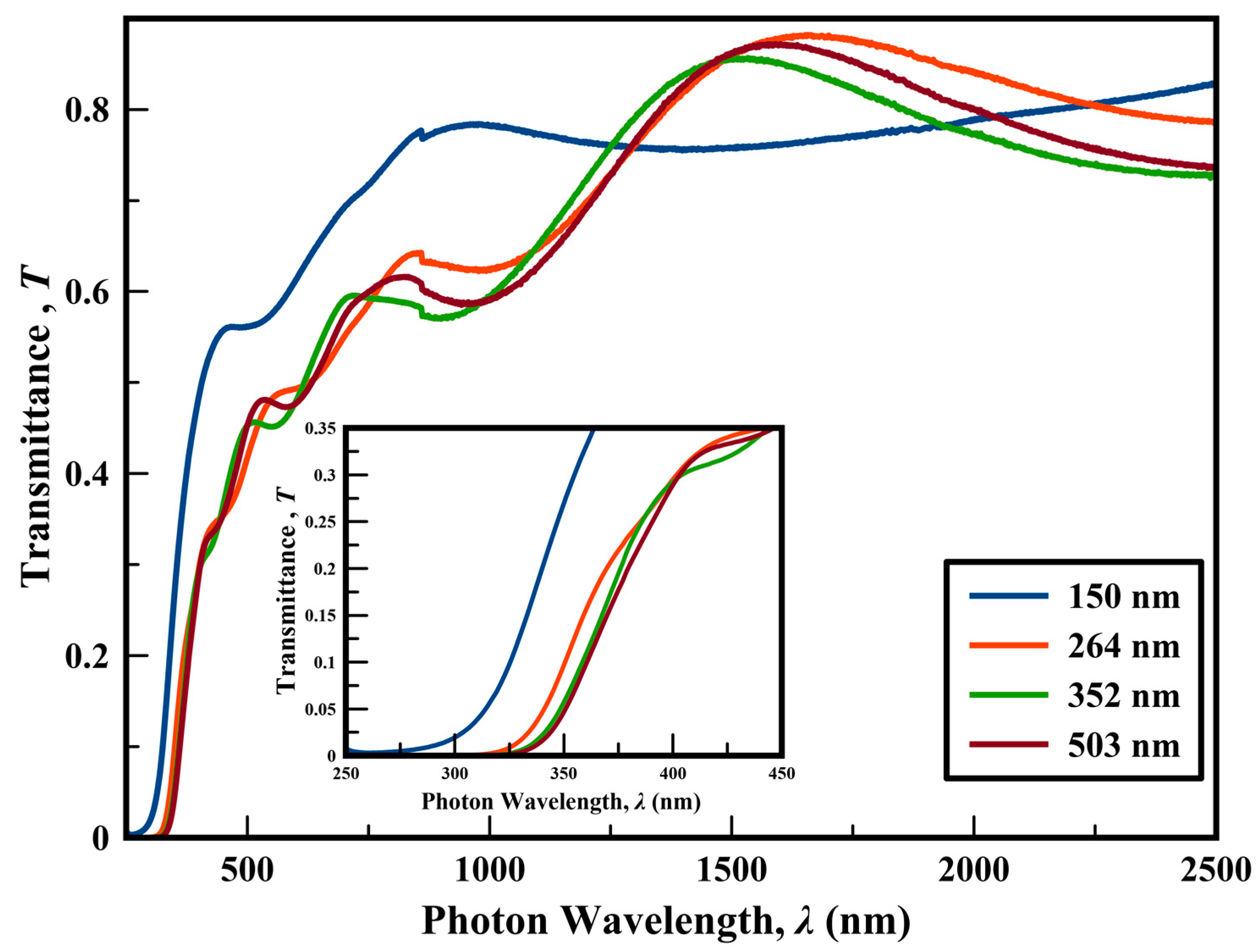
3.3. Optical Properties of Nickel Oxide Films

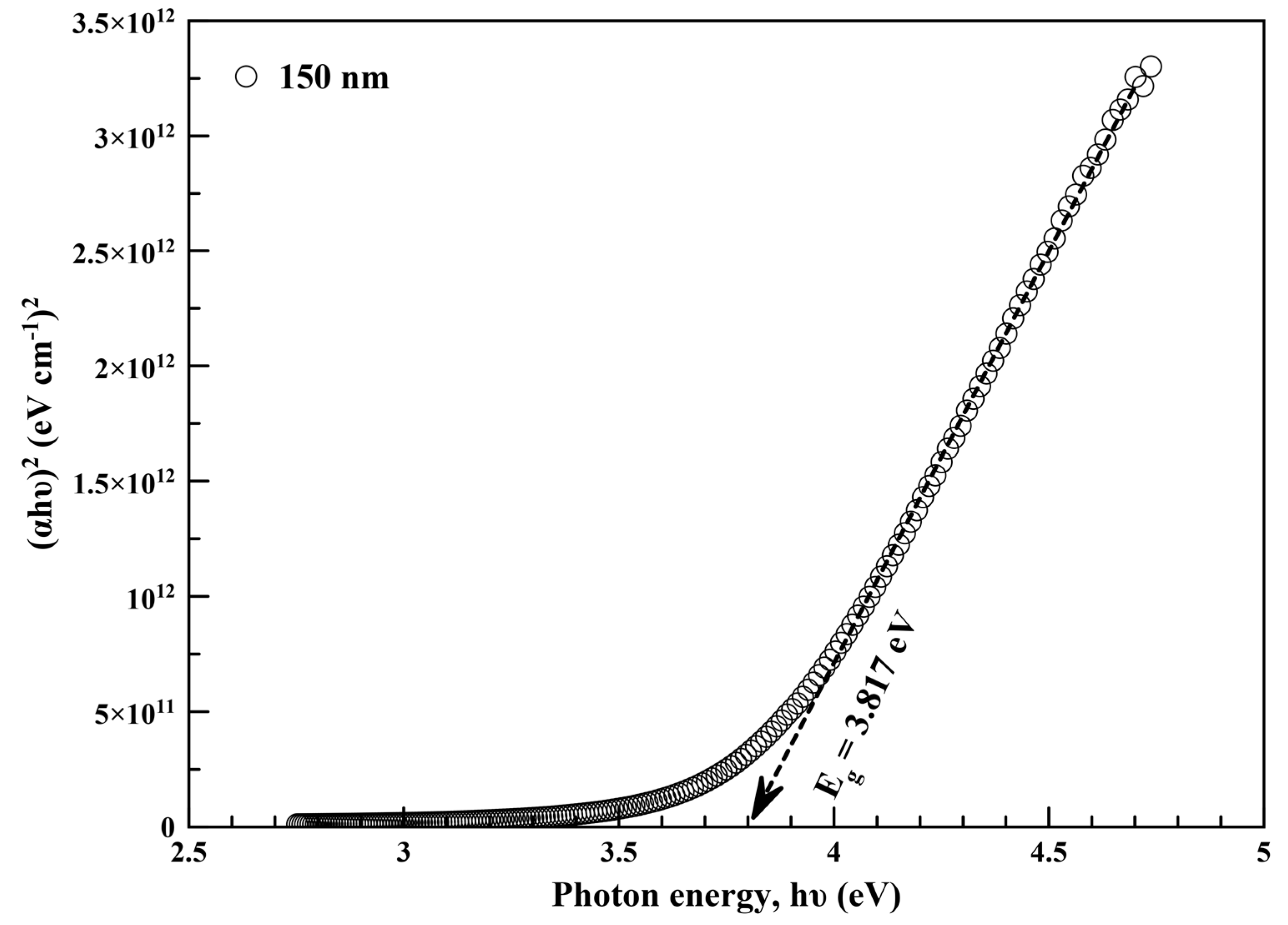
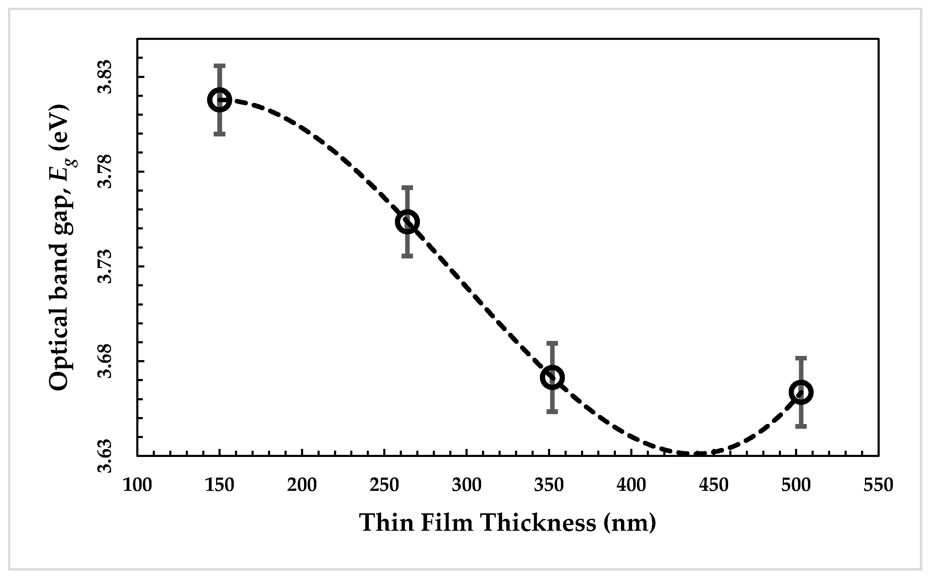
3.3.1. Optical Transmittance and Optical Band Gap

The optical transmittance, T, of nickel oxide thin films is shown in Figure 4. The optical transference is observed through all samples, indicating the good quality and homogeneity of the films. The inset figure shows the displacement of the absorption edge toward a higher wavelength. Therefore, the expected optical band gap values decreased as the thin film thickness increased.
For the estimation of the optical energy band gap, Eg, and the transition order, q, the following procedure is applied:
The optical energy band gap depends on the absorption coefficient, α according to the following equation [26]:
( α h υ ) = β ( h υ E g ) q
where β represents the energy independent constant, and α is deduced from the expression α = 1 t ln ( 1 T ) . The optical transition order, q, is then to be either ½ for direct transition or 2 for indirect transition. It is agreed that in the case of the crystalline materials, the optical transition is almost a direct transition; q = ½ in Equation (3). Therefore, the resulting plot of (αhυ)2 vs. hυ is a curve with a straight-line portion [27,28,29]. The intersection of this linear portion with the hυ axis is analogous to the value of the energy band gap as seen in Figure 5 for the film thickness of 150 nm.
The estimated optical band gap values have a similar trend, as shown in Figure 5, which decreases as the thin film thickness increases, as shown in Figure 6. The values of the optical band gap changed from 3.817 to 3.663 eV as the film thickness increased from 150 to 503 nm (red shift). The previous investigation of nickel oxide thin films prepared at different oxygen flow rates by Hammad et al. [10] showed that at an oxygen gas rate of 10 SCCM with a thickness of 141 nm has a band gap value of 3.74 eV. Therefore, the thickness changed in the range of 141 to 150 nm and by increasing the deposition time/film thickness, a red shift occurred, up to a higher thickness of 503 nm.

3.3.2. Refractive Index and High-Frequency Dielectric Constant

The linear refractive index, no, is directly proportional to the optical band gap, Eg, from the Moss relation [30]:
n o = 95 E g 1 4
Moreover, the high-frequency dielectric constant, ε, and the static dielectric constant, εo, are also correlated with the optical band gap according to Adachi as follows [31]:
ε = 11.26 1.42 E g
ε 0 = 18.52 3.08 E g
The presented data of the refractive index, no, the high frequency dielectric constant, ε, and the static dielectric constant, εo, are presented in Table 3. These data agree with the study obtained by El-Nahass et al. [32] for nickel oxide films obtained via electron beam evaporation.

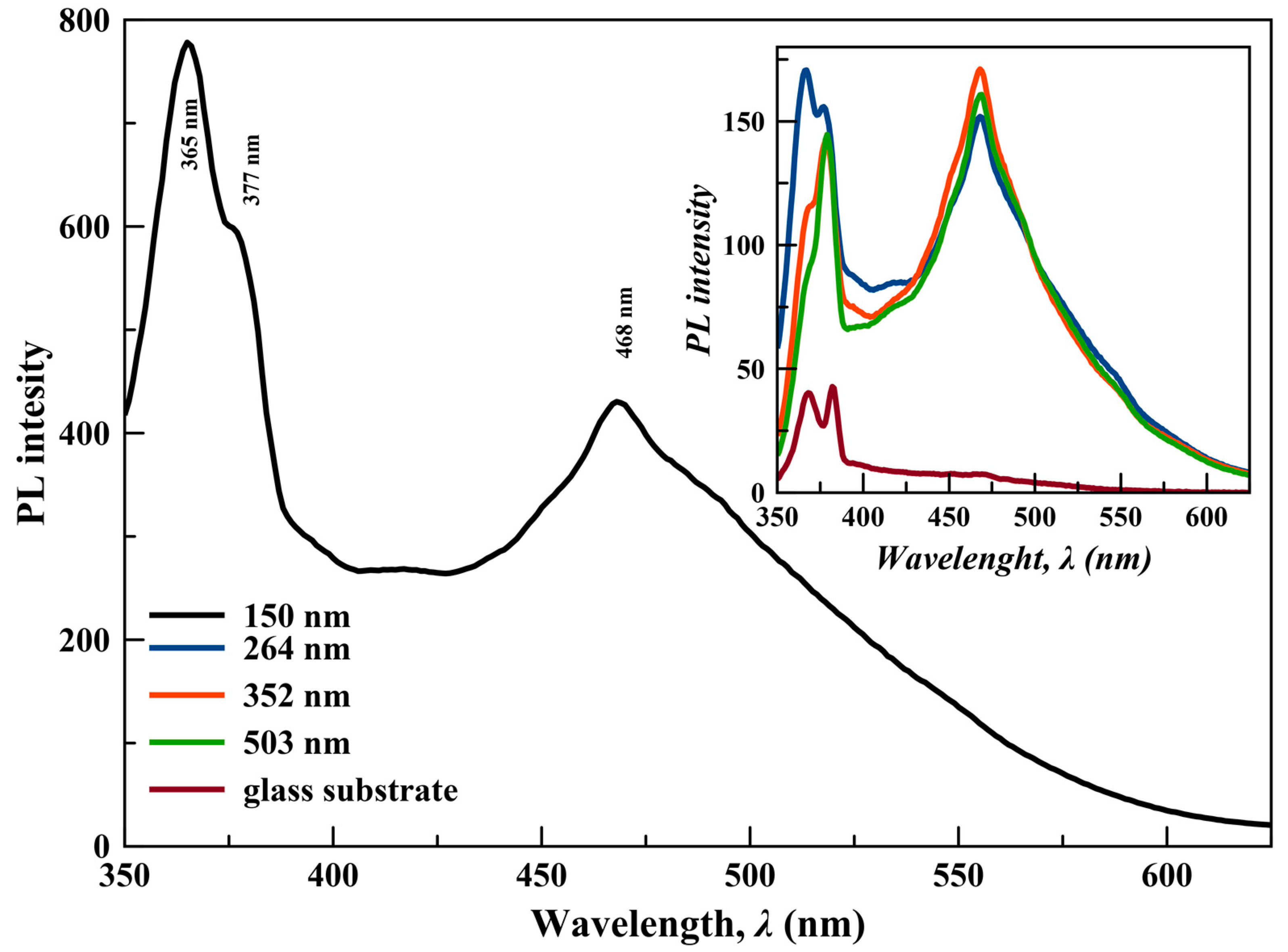
3.4. Photoluminescence Properties

Figure 7 shows the PL spectra of NiOx for a film thickness of 150 nm, while the inset figure shows the PL behavior for the other film thicknesses from 264 to 503 nm as well as the glass substrate. The photoluminescence intensity descends as the film thickness grows and is higher in the intensity than the glass substrate. Three characteristic peaks/shoulders are observed for all films, located at 365, 377, and 468 nm, respectively. Indeed, the PL of the glass substrate has two peaks, at 370 and 385 nm. No further peaks occur in the range of 450–500 nm. This means that the PL peak at 468 nm is for NiOx and not for the glass substrate. Moreover, the coating of NiOx on the glass substrate shifts the peak from 370 to 365 nm and from 385 to 377 nm, forming a broad peak with a shoulder instead of two distinct peaks, as observed for the glass substrate. This could be explained as the superposition of the PL peaks of NiO and the glass substrate.
Hence, PL investigation confirmed the structural change in the NiOx films. The peaks at 365 and 377 nm suggest exciton-exciton scattering in the UV emission [10,33]. The peak at 468 nm is correlated with the recombination of electron-holes in the vacancies of the Ni and O lattice [10,34,35,36]. The photoluminescence spectra are correlated with the particle size of the prepared films. As the particle size decreases, the PL intensity is also decreased. This assumption was suggested and confirmed by Musevi et al. [34] when they investigated the particle size distribution and correlated it with the PL spectra. As the film’s thickness grows, and the presence of the non-stoichiometric ratio is realized, the defects or vacancies increase, leading to the decreasing value of the PL intensity, as well as the transmittance spectra.

4. Conclusions

Sputtered nickel oxide thin films at a fixed oxygen flow rate of 10 SCCM and at different deposition times proved the trigonal phase of nickel oxide due to the vacancies in the nickel lattice and the excess of oxygen gas. Therefore, the present sputtering process suggests the non-stoichiometric behavior of nickel oxide. The crystallites are grown through planes (101) and (110). However, the crystallite growth on plan (101) is predominant through the film thickness growing. Spherical particles are grown and their size decreases as the film thickness increases. The absorption edge of the prepared films is red shifted towards a higher wavelength (or at higher thicknesses), and the optical band gap values are then decreased as the film thickness increases. The refractive index and the dielectric constants are proportional to the optical band gap values. Photoluminescence spectra showed that defects are created in the nickel oxide lattice. Moreover, this is strongly dependent on the film’s morphology and the particle size. The PL intensity decreases as the film thickness increases, as well as when the particle size decreases. This means that the PL behavior of NiOx is dominated by both the film morphology and the film thickness.

Author Contributions

Conceptualization, A.H.H., and M.S.A.-w.; methodology, A.H.H.; software, S.V., and A.R.A.; validation, A.H.H., and M.S.A.-w.; formal analysis, S.V., and A.R.A; investigation, A.H.H.; resources, M.S.A.-w.; data curation, A.H.H.; writing—original draft preparation, M.S.A.-w.; writing—review and editing, A.H.H.; visualization, A.H.H.; supervision, A.H.H.; project administration, A.H.H.; funding acquisition, A.H.H.

Funding

This research was funded by the Deanship of Scientific Research (DSR), King Abdulaziz University, Jeddah grant number (D-100-903-1440).

Acknowledgments

The authors, therefore, gratefully acknowledge the DSR technical and financial support.

Conflicts of Interest

The authors declare no conflict of interest.

References

  1. Fujii, E.; Tomozawa, A.; Torii, H.; Takayama, R. Preferred orientations of NiO films prepared by plasma-enhanced metalorganic chemical vapor deposition. Jpn. J. Appl. Phys. 1996, 35, L328–L330. [Google Scholar] [CrossRef]
  2. Tsuda, N.; Nasu, K.; Fujimori, A.; Siratori, K. Electronic Conduction in Oxides; Springer: Berlin/Heidelberg, Germany, 2000. [Google Scholar]
  3. Song, Z.; Bourgeteau, T.; Raifuku, I.; Bonnassieux, Y.; Johnson, E.; Ishikawa, Y.; Foldyna, M.; i Cabarrocas, P.R.; Uraoka, Y. Structural study of NiOx thin films fabricated by radio frequency sputtering at low temperature. Thin Solid Films 2018, 646, 209–215. [Google Scholar] [CrossRef]
  4. Kofstad, P. Defects and transport properties of metal oxides. Oxid. Met. 1995, 44, 3–27. [Google Scholar] [CrossRef]
  5. Passerini, S.; Scrosati, B. Characterization of nonstoichiometric nickel oxide thin-film electrodes. J. Electrochem. Soc. 1994, 141, 889. [Google Scholar] [CrossRef]
  6. Lee, S.-H.; Tracy, C.E.; Roland Pitts, J. Effect of nonstoichiometry of nickel oxides on their supercapacitor behavior. Electrochem. Solid-State Lett. 2004, 7, A299–A301. [Google Scholar] [CrossRef]
  7. Manceriu, L.M.; Colson, P.; Maho, A.; Eppe, G.; Nguyen, N.D.; Labrugere, C.; Rougier, A.; Cloots, R.; Henrist, C. Straightforward prediction of the Ni1−xO layers stoichiometry by using optical and electrochemical measurements. J. Phys. D Appl. Phys. 2017, 50, 225501. [Google Scholar] [CrossRef]
  8. Kwon, D.-H.; Lee, S.R.; Choi, Y.S.; Son, S.-B.; Oh, K.H.; Char, K.; Kim, M. Observation of the Ni2O3 phase in a NiO thin-film resistive switching system. Phys. Status Solidi Rapid Res. Lett. 2017, 11, 1700048. [Google Scholar] [CrossRef]
  9. Zhu, Z.; Ping, J.; Huang, X.; Hu, J.; Chen, Q.; Ji, X.; Banks, C.E. Hexagonal nickel oxide nanoplate-based electrochemical supercapacitor. J. Mater. Sci. 2012, 47, 503–507. [Google Scholar] [CrossRef]
  10. Hammad, A.H.; Abdel-wahab, M.S.; Vattamkandathil, S.; Ansari, A.R. Influence the oxygen flow rate on the film thickness, structural, optical and photoluminescence behavior of DC sputtered NiOx thin films. Phys. B Condens. Matter 2019, 568, 6–12. [Google Scholar] [CrossRef]
  11. Garcia-Miquel, J.; Zhang, Q.; Allen, S.; Rougier, A.; Blyr, A.; Davies, H.; Jones, A.; Leedham, T.; Williams, P.; Impey, S. Nickel oxide sol–gel films from nickel diacetate for electrochromic applications. Thin Solid Films 2003, 424, 165–170. [Google Scholar] [CrossRef]
  12. Sawaby, A.; Selim, M.S.; Marzouk, S.Y.; Mostafa, M.A.; Hosny, A. Structure, optical and electrochromic properties of NiO thin films. Phys. B Condens. Matter 2010, 405. [Google Scholar] [CrossRef]
  13. Danial, A.S.; Saleh, M.M.; Salih, S.A.; Awad, M.I. On the synthesis of nickel oxide nanoparticles by sol–gel technique and its electrocatalytic oxidation of glucose. J. Power Sources 2015, 293, 101–108. [Google Scholar] [CrossRef]
  14. Sagadevan, S.; Rajesh, S.; Das, I. Studies on nanocrystalline nickel oxide thin films for potential applications. Mater. Today Proc. 2017, 4, 4123–4129. [Google Scholar] [CrossRef]
  15. Sun, J.; Lu, J.; Li, B.; Jiang, L.; Chesman, A.S.R.; Scully, A.D.; Gengenbach, T.R.; Cheng, Y.-B.; Jasieniak, J.J. Inverted perovskite solar cells with high fill-factors featuring chemical bath deposited mesoporous NiO hole transporting layers. Nano Energy 2018, 49, 163–171. [Google Scholar] [CrossRef]
  16. Das, M.R.; Mukherjee, A.; Mitra, P. Structural, optical and ac electrical characterization of CBD synthesized NiO thin films: Influence of thickness. Phys. E Low Dimens. Syst. Nanostructures 2017, 93, 243–251. [Google Scholar] [CrossRef]
  17. Agrawal, A.; Habibi, H.R.; Agrawal, R.K.; Cronin, J.P.; Roberts, D.M.; Caron-Popowich, R.; Lampert, C.M. Effect of deposition pressure on the microstructure and electrochromic properties of electron-beam-evaporated nickel oxide films. Thin Solid Films 1992, 221, 239–253. [Google Scholar] [CrossRef]
  18. Sahu, D.R.; Wu, T.-J.; Wang, S.-C.; Huang, J.-L. Electrochromic behavior of NiO film prepared by e-beam evaporation. J. Sci. Adv. Mater. Devices 2017, 2, 225–232. [Google Scholar] [CrossRef]
  19. Conell, R.S.; Corrigan, D.A.; Powell, B.R. The electrochromic properties of sputtered nickel oxide films. Sol. Energy Mater. Sol. Cells 1992, 25, 301–313. [Google Scholar] [CrossRef]
  20. Zhao, Y.; Wang, H.; Yang, F.; Zhen, Z.; Li, X.; Li, Q.; Li, J. Influence of growth temperature on structure, optical and electrical properties of nickel oxide films by magnetron sputtering. Vacuum 2018, 151, 163–166. [Google Scholar] [CrossRef]
  21. Inoue, N.; Yasuoka, Y. Properties of nickel oxide films grown by sputter oxidation. Vacuum 1984, 34, 687–691. [Google Scholar] [CrossRef]
  22. Widjonarko, N.E.; Ratcliff, E.L.; Perkins, C.L.; Sigdel, A.K.; Zakutayev, A.; Ndione, P.F.; Gillaspie, D.T.; Ginley, D.S.; Olson, D.C.; Berry, J.J. Sputtered nickel oxide thin film for efficient hole transport layer in polymer–fullerene bulk-heterojunction organic solar cell. Thin Solid Films 2012, 520, 3813–3818. [Google Scholar] [CrossRef]
  23. Gordillo, G.; Flórez, J.M.; Hernández, L.C. Preparation and characterization of CdTe thin films deposited by CSS. Sol. Energy Mater. Sol. Cells 1995, 37, 273–281. [Google Scholar] [CrossRef]
  24. Sakaliūnienė, J.; Čyvienė, J.; Abakevičienė, B.; Dudonis, J. Investigation of structural and optical properties of GDC thin films deposited by reactive magnetron sputtering. Acta Phys. Pol. A 2011, 120, 63–65. [Google Scholar] [CrossRef]
  25. Nasser, S.; Afify, H..; El-Hakim, S.; Zayed, M. Structural and physical properties of sprayed copper–zinc oxide films. Thin Solid Films 1998, 315, 327–335. [Google Scholar] [CrossRef]
  26. Davis, E.A.; Mott, N.F. Conduction in non-crystalline systems V. Conductivity, optical absorption and photoconductivity in amorphous semiconductors. Philos. Mag. 1970, 22, 0903–0922. [Google Scholar] [CrossRef]
  27. Abdel-wahab, M.S.; Jilani, A.; Alshahrie, A.; Hammad, A.H. Impact of titanium ions in the hexagonal nanostructured ZnO thin films. J. Mater. Sci. Mater. Electron. 2018, 29, 3056–3065. [Google Scholar] [CrossRef]
  28. Hammad, A.H.; Abdel-wahab, M.S.; Vattamkandathil, S.; Ansari, A.R. Structural and optical properties of ZnO thin films prepared by RF sputtering at different thicknesses. Phys. B Condens. Matter 2018, 540, 1–8. [Google Scholar] [CrossRef]
  29. Hammad, A.H.; Abdel-wahab, M.S. Investigation the phase transformation of sputtered molybdenum oxide thin films and their correlation with the film thickness. Optik 2018, 154, 777–784. [Google Scholar] [CrossRef]
  30. Moss, T.S. Relations between the refractive index and energy gap of semiconductors. Phys. Status Solidi 1985, 131, 415–427. [Google Scholar] [CrossRef]
  31. Optical Properties. In Properties of Group-IV, III-V and II-VI Semiconductors; Adachi, S. (Ed.) John Wiley & Sons, Ltd.: Chichester, UK, 2005; pp. 211–281. [Google Scholar]
  32. El-Nahass, M.M.; Emam-Ismail, M.; El-Hagary, M. Structural, optical and dispersion energy parameters of nickel oxide nanocrystalline thin films prepared by electron beam deposition technique. J. Alloy. Compd. 2015, 646, 937–945. [Google Scholar] [CrossRef]
  33. Mohseni Meybodi, S.; Hosseini, S.A.; Rezaee, M.; Sadrnezhaad, S.K.; Mohammadyani, D. Synthesis of wide band gap nanocrystalline NiO powder via a sonochemical method. Ultrason. Sonochem. 2012, 19, 841–845. [Google Scholar] [CrossRef] [PubMed]
  34. Musevi, S.J.; Aslani, A.; Motahari, H.; Salimi, H. Offer a novel method for size appraise of NiO nanoparticles by PL analysis: Synthesis by sonochemical method. J. Saudi Chem. Soc. 2016, 20, 245–252. [Google Scholar] [CrossRef] [Green Version]
  35. Kumari, L.; Li, W.Z.; Vannoy, C.H.; Leblanc, R.M.; Wang, D.Z. Vertically aligned and interconnected nickel oxide nanowalls fabricated by hydrothermal route. Cryst. Res. Technol. 2009, 44, 495–499. [Google Scholar] [CrossRef]
  36. Mrabet, C.; Ben Amor, M.; Boukhachem, A.; Amlouk, M.; Manoubi, T. Physical properties of La-doped NiO sprayed thin films for optoelectronic and sensor applications. Ceram. Int. 2016, 42, 5963–5978. [Google Scholar] [CrossRef]
Figure 1. XRD of NiOx thin films at different thicknesses.
Coatings 09 00615 g001
Figure 2. The variation of the crystallite size as a function of thin film thickness.
Coatings 09 00615 g002
Figure 3. 2D and 3D AFM of NiOx thin films at different film thicknesses.
Coatings 09 00615 g003
Figure 4. Optical transmittance of nickel oxide thin films.
Coatings 09 00615 g004
Figure 5. Optical band gap determination of 150 nm NiOx thin film.
Coatings 09 00615 g005
Figure 6. Dependence the optical band gap on the film thickness.
Coatings 09 00615 g006
Figure 7. Photoluminescence spectra of NiOx thin films at different film thicknesses.
Coatings 09 00615 g007
Table 1. Film thickness (nm), the crystallite size on plane (101) and (110) (nm), and the texture coefficient Tx for planes (101) and (110) for trigonal nickel oxide thin films.
Deposition Time (s)Film Thickness (nm)Crystallite Size, D (101) (nm)Crystallite Size, D (110) (nm)Texture Coefficient, Tx (101)Texture Coefficient, Tx (110)Full Width at Half Maximum FWHM (110)
120015018.2718.131.7910.3280.51
180026420.0617.821.910.7560.54
210035219.4416.421.3921.1650.59
240050319.76161.7340.4750.62
Table 2. Grain size and the film roughness values for NiO0.96 thin films.
Film Thickness (nm)Grain Size (nm)Film Roughness (nm)
15046.851.11
26439.601.56
35234.251.06
50330.671.94
Table 3. Some optical parameters for NiO0.96 thin films at different thicknesses.
Film Thickness (nm)150264352503
Optical Band Gap, Eg (eV)3.8173.7553.6713.664
Refractive Index, no2.2342.2432.2552.257
High Frequency Dielectric Constant, ε∞5.845.936.0476.058
Static Dielectric Constant, εo6.7616.967.2127.24
Optical Parameters Obtained from Ref. [29]Eg = 3.849 (eV)no = 2.1ε∞ = 5.408

