Abstract
High-density ruthenium (Ru) thin films were deposited using Ru(EtCp)2 (bis(ethylcyclopentadienyl)ruthenium) and oxygen by thermal atomic layer deposition (ALD) and compared to magnetron sputtered (MS) Ru coatings. The ALD Ru film growth and surface roughness show a significant temperature dependence. At temperatures below 200 °C, no deposition was observed on silicon and fused silica substrates. With increasing deposition temperature, the nucleation of Ru starts and leads eventually to fully closed, polycrystalline coatings. The formation of blisters starts at temperatures above 275 °C because of poor adhesion properties, which results in a high surface roughness. The optimum deposition temperature is 250 °C in our tool and leads to rather smooth film surfaces, with roughness values of approximately 3 nm. The ALD Ru thin films have similar morphology compared with MS coatings, e.g., hexagonal polycrystalline structure and high density. Discrepancies of the optical properties can be explained by the higher roughness of ALD films compared to MS coatings. To use ALD Ru for optical applications at short wavelengths (λ = 2–50 nm), further improvement of their film quality is required.
1. Introduction
Ultrathin metal films are essential for numerous applications, especially in microelectronics [1], heterogeneous catalysis [2], soft X-ray optics, and sensing. Ruthenium, as a relatively low-cost noble metal, is an attractive material when high oxidation resistance is needed [3]. Smooth and high-density Ru thin films are a preferred solution, for example, as electrodes for dynamic random access memories (DRAM) [4,5,6,7], metal-oxide-semiconductor field-effect transistors (MOSFET) [8], metal-insulator-metal capacitors [9,10], and grazing-incidence soft X-ray mirrors [11]. The atomic layer deposition (ALD) technology enables pinhole-free and conformal films with sub-nanometer thickness control. Since conventional physical vapor deposition (PVD) technologies cannot realize conformal coatings on complex shaped substrates, ALD is being considered as a promising technology for optical coatings. High-efficiency metal wire polarizers for UV spectral range have already been realized based on frequency doubling technique with iridium (Ir) coatings by ALD [12,13]. Iridium ALD coating has been also applied for Fresnel zone plates for X-ray microscopes at 1 keV synchrotron radiation [14]. Although ALD of Ru processes has been widely investigated for their electronic properties [2,6,7,8,9,15,16,17,18,19], their optical properties have not been analyzed yet. The large interest for Ru ALD arises since it is considered as a favorable capacitor electrode in DRAM [3,4,6,18], as gates in metal oxide semiconductor transistors [5,8], or is applied as nucleation seed layers for copper interconnect formation [19]. As an optical coating, Ru is currently realized for capping layers [3,20,21] and grazing incidence mirrors [22,23,24,25] by magnetron sputtering (MS).
This article presents the optical and structural properties of Ru ALD in the soft X-ray and XUV (extreme UV) spectral range. Furthermore, the coating properties are compared with conventional sputtered Ru films and the potential of the ALD technology for optical applications is discussed.
2. Experimental
Ru thin film deposition was performed with an Oxford Instruments OpAL open load reactor tool. In this study, Ru(EtCp)2 (bis(ethylcyclopentadienyl)ruthenium, Strem Chemicals, Kehl, Germany) and O2 were used as metalorganic precursor and co-reactant, respectively. Ru(EtCp)2 as a liquid precursor has a relatively high vapor pressure of 0.24 mbar at 80 °C [26]. This temperature was applied to bubble the precursor with 150 sccm argon (Ar) gas flow into the ALD reactor. Under a working pressure of approximately 0.1 mbar, the coatings were fabricated in a thermal ALD process at substrate temperatures between 200 °C and 300 °C. Major reaction products during this ALD process are carbon dioxide (CO2) and water (H2O). The overall chemical reaction can be suggested as:
Ru(EtCp)2 (g) + 37/2 O2 (g) → Ru (s) + 9 H2O (g) + 14 CO2 (g)
Growth rate experiments of the Ru films were performed at a deposition temperature of 250 °C. The ALD cycle consists of four repeated steps: Ru(EtCp)2 precursor pulse, precursor purge with Ar (150 sccm), co-reactant pulse with 50 sccm O2, and a final purge with 150 sccm Ar flow. The optimized time for each step was constant at 2 s, 4 s, 3 s, and 4 s, respectively. Furthermore, a plasma enhanced ALD (PEALD) process was tested. Therefore, O2 plasma was ignited with 100 W RF power at 100 sccm flow rate. The substrate was exposed for three seconds to the O2 plasma instead of the thermally activated O2 gas flow. Super-polished silicon (Si) wafers with a crystal orientation of (100) and amorphous fused silica (SiO2) were used as conventional substrates for optical coatings.
For comparison, Ru coatings were fabricated on the DC-magnetron sputtering system NESSY 3 [27]. In this industrial system, coatings were deposited in an Ar atmosphere on Si substrates with a working pressure of 10−3 mbar and a source power of 500 W.
All samples produced were measured by grazing incidence X-ray reflectometry (XRR) with Cu-Kα radiation (λ = 0.154 nm) to characterize the coating properties. The XRR data were fitted with a simple single layer model (Ru on substrate, whereby the roughness of the coating is also considered) using the Leptos 7 software package (Bruker Corporation) [28]. The extracted simulation results provide information on the coating thickness, coating density, and surface roughness. The same measurement setup was used for X-ray diffraction experiments (XRD). The crystal sizes were estimated according to the Scherrer equation [29].
Furthermore, the surface was investigated with a Carl Zeiss Σigma scanning electron microscope (SEM, Carl Zeiss, Oberkochen, Germany) with a constant acceleration voltage of 10 kV and energy dispersive X-ray analysis (EDX) for chemical characterization. Surface roughness analysis was additionally carried out through atomic force microscopy (AFM, Dimension 3100 with Nanoscope IV controller, Digital Instruments, Santa Barbara, CA, USA) measurements.
The XUV reflectometry (XUVR) was carried out by the Physikalisch Technische Bundesanstalt (PTB, Bessy II, Beamline PTB-EUV, Berlin, Germany) [30] at a fixed grazing incidence angle of 10° varying the wavelength between 2 nm and 25 nm. The reflectivity curves were simulated with the IMD-software [31] using the optical constants of Henke et al. [32]. Similar to the XRR simulations, a single-layer model has initially been applied, but had to be extended by a thin RuO2 and C layer.
The surface composition was studied with X-ray photoelectron spectroscopy (XPS, XR 50 M X-ray source with FOCUS 500 monochromator, SPECS Surface Nano Analysis GmbH, Berlin, Germany) using an ultrahigh vacuum (UHV) surface analysis system. The photoelectrons were excited by monochromatic Al-Kα radiation (E = 1486.71 eV) under 55° angle of incidence and detected with a PHOIBOS 150 hemispherical electron analyzer (SPECS Surface Nano Analysis GmbH, Berlin, Germany).
Additionally, an Auger electron spectroscopy (AES, Varian Vacuum Division, Palo Alto, CA, USA) depth profile was performed with an Auger cylindrical mirror spectrometer. A focused 5 keV electron beam under an angle of incidence of 30° and a cylindrical mirror analyzer (CMA) were used. Sputtering was carried out with krypton (Kr) at an energy of 2 keV and a current of 10 µA.
3. Results
Atomic layer deposition of Ru has been reported using several metalorganic precursors. Hämäläinen et al. presented a review of the reported Ru ALD processes with various precursors [33]. They summarized growth rates, deposition temperatures and the evaporation temperature of different precursors relating to the corresponding co-reactants. Besides Ru(Cp)2 [6,34] and Ru(Thd)3 [33,35], Ru(EtCp)2 [5,10,34,36] is the most commonly used precursor. Its flexible deposition properties have led to the choice of Ru(EtCp)2 to start here the optical coating development. Besides thermal and plasma enhanced ALD, the precursor enables the deposition with a wide selection of co-reactants, e.g., air [6], O2 [26,34], ozone (O3) [10], ammonia (NH3) [19,34], and hydrogen (H2) [5]. The main by-products of the chosen process (Ru(EtCp)2 and O2) are water and carbon dioxide [37] (see Equation (1)) and thus it fulfills safety requirements. Furthermore, the liquid precursor Ru(EtCp)2 is readily available in adequate ALD bubblers for precursor delivery.
3.1. Structural Properties
Immediately after deposition, all coatings were characterized by XRR to determine the density (ρ), roughness (σ), and film thickness (z) without major influence of contaminations.
The experimental data and the corresponding simulation are presented in Figure 1. As shown, a simple simulation model (single Ru layer on Si-substrate) describes the experimental data very well. After 1500 cycles at 250 °C, the Ru grows to a z = 57.5 nm thick film with a surface roughness of σ = 2.6 nm. At comparable temperatures of 275 °C to 300 °C, other authors reported an even higher surface roughness from 3.7 nm [34] up to 13.9 nm [10] of thermally deposited Ru. Furthermore, the Ru ALD layer exhibits a high density of ρ = 12.3 g·cm−3 comparable to the bulk Ru value of 12.45 g·cm−3 [38].
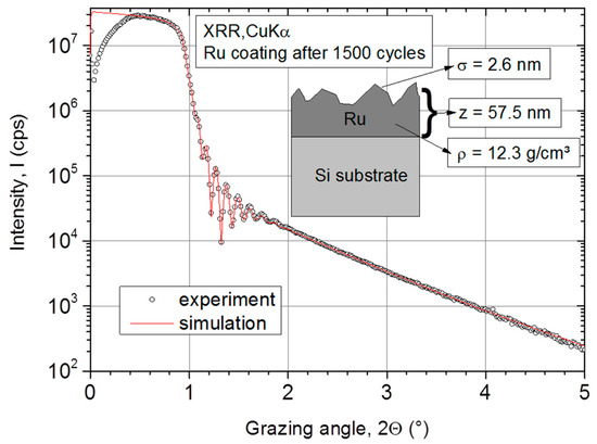
Figure 1.
X-ray reflectometry (XRR) measurement on atomic layer deposition (ALD) Ru layer and corresponding simulation with a simple two-layer model (substrate + Ru thin film).
To determine the growth rate per cycle (GPC), processes were carried out with 500 cycles up to 3000 cycles and the films were thoroughly characterized. Figure 2 points out a linear thickness evolution with increasing number of ALD cycles. The GPC was determined by a linear fit to (0.047 ± 0.002) nm/cycle on a Si substrate and (0.049 ± 0.002) nm/cycle on fused silica, respectively. Compared with other ALD processes using Ru(EtCp)2 as a precursor, the determined GPCs are of the same magnitude. Wojcik et al. reported a growth rate of 0.037 nm/cycle with a Ru(EtCp)2 PEALD process [39] and Park et al. 0.075 nm/cycle with a thermal process [34]. A higher growth rate of 0.12 nm/cycle was achieved with O3 as co-reactant [10].
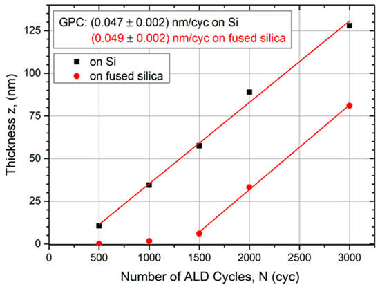
Figure 2.
Evolution of Ru film thickness determined by XRR measurements as function of the number of ALD cycles on different substrates. After a nucleation delay, the growth rate per cycle (GPC) becomes constant for both substrate materials.
Figure 2 indicates a nucleation delay since the linear fit does not cross the origin until the growth rate becomes constant. This delay lasts longer for amorphous fused silica substrates compared with Si substrates. Following the linear fit in Figure 2, the linear growth regime starts after approximately 250 cycles on Si and after 1350 cycles on SiO2, respectively. An ALD review by George indicates that ALD metals prefer to form clusters on oxide surfaces [40]. Depending on the substrate material, it takes a certain amount of ALD cycles until the first metal layer is fully closed and the growth becomes linear per cycle. Hämäläinen et al. reported that this nucleation delay for Ru can last up to hundreds of cycles [33], as our observation also indicates. The initial density of nucleation sites plays a critical role in the formation of Ru thin films and is higher on Si than on SiO2. On noble metal substrates, such as platinum (Pt) and palladium (Pd), no nucleation delay was found by Lu et al. [5].
Nevertheless, all ALD coatings show a high density of (12.3 ± 0.1) g·cm−3 by XRR independent of their thickness. Repeated XRR measurements show identical curves three months past deposition. Thus, high coating stability is assumed due to identical XRR results. High-density coatings are important for the optical properties in the soft X-ray and XUV spectral range [41]. Kim et al. report a density of ρ = 11.9 g·cm−3 by XRR investigations [10] although they used O3 as a more reactive co-reactant. The highest Ru coating density of 12.7 g·cm−3, achieved with an O2 based ALD process, was reported by Manke et al. [42] at temperatures of Tdep = 450 °C. In addition to the density, a low surface roughness is also essential for high reflective properties in optical applications. We have determined a strong influence of the deposition temperature Tdep on the film growth and thus the surface roughness.
Figure 3 presents film surface morphologies after 500 cycles deposited at different temperatures. No deposition was observed at temperatures below Tdep < 200 °C. The deposition started at Tdep = 230 °C. However, the nucleation delay was so high that even after 500 cycles the layer was not fully covering the substrate and Ru nanoparticles were clearly visible. The black background corresponds to the Si substrate surface. The small white areas on top are Ru nuclei with a diameter of approximately 6–20 nm. The growth rate rises with an increasing temperature of Tdep = 250 °C. At this point, the complete surface is covered with Ru crystals and results in a film thickness of z = 17 nm. Furthermore, the estimated crystal size is of a similar magnitude (20–30 nm). At a higher deposition temperature of Tdep = 300 °C, the lateral crystal size grows further to 25–40 nm. Besides a larger film thickness (z = 35 nm by XRR) caused by a higher growth rate, a possible reason for larger grains is the higher substrate temperature itself. This increases the mobility of the Ru atoms and thus they can reach places at a favorable energetic state, e.g., the crystal lattice.
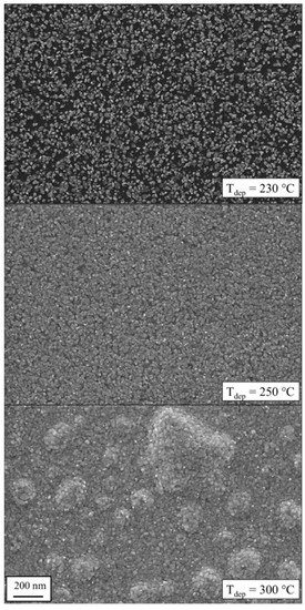
Figure 3.
Scanning electron microscopy (SEM) images of Ru layers at different deposition temperatures after 500 ALD cycles. While no deposition was observed below Tdep = 200 °C, blistering occurred at higher temperatures. A temperature optimum was found at 250 °C.
Furthermore, the formation of blisters at deposition temperature of 300 °C can be seen in Figure 3. These large blisters consist of air pockets. This phenomenon was also reported by Kim et al. for a Ru(EtCp)2–O2 process [10]. For Ru deposition at Tdep = 275 °C, they reported a formation of blisters that led to a significant surface roughness of approximately 14 nm [10]. Other O2 based metal ALD, e.g., Ir [43], show also the effect of blistering, whereby improving the process parameters (e.g., long purge time) significantly minimized the appearance of defects. Gadkari et al. described that the blistering can be caused by the combination of stress and a weak film-substrate adhesion [44]. Nevertheless, we also detected that the film adhesion became worse and the coating could easily be scratched. Thus, these coatings deposited at high temperatures are not suitable for optical applications.
As shown in Figure 3, all coatings demonstrate a crystalline growth. Therefore, additional XRD-investigations have been carried out to study the crystallinity of the Ru ALD coatings in detail. Figure 4 shows the diffraction pattern of a 57 nm thick coating on a Si substrate deposited at the optimized temperature of 250 °C. For comparison, an MS coating with equivalent thickness is additionally presented.
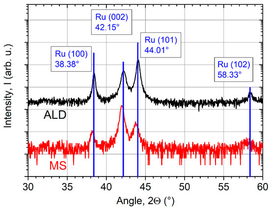
Figure 4.
X-ray diffraction (XRD) pattern of ALD (z = 57 nm) and magnetron sputtered (MS) (z = 50 nm) Ru coatings on Si substrates with corresponding phase analysis. Diffraction peaks of the MS coating are slightly shifted to smaller angles indicating film stress.
Both coatings consist of hexagonal polycrystals [45]. Three peaks can be clearly identified at the angles of 38°, 42°, and 44°. The fourth peak at 58° is only indicated because of its low intensity. The blue solid lines show the intensity distribution of each peak for a randomly oriented powder sample. This indicates that both coatings are randomly oriented with the Ru polycrystalline structure oriented in the [100], [002] and [101] orientations in the growth direction. Further, the peaks of the sputtered coating are slightly shifted to smaller angles. These findings suggest that the coating is under compressive stress. Alagoz et al. report on high compressive stresses of several GPa in Ru films by MS [46]. The ALD sample matches the diffraction database values perfectly. Therefore, low film stress is expected. The film stress, reported by Kim et al. based on a Ru(EtCp)2 and O2 process, was also low with a value of 88 MPa [10].
Figure 5 summarizes the evolution of grain size and roughness with increasing film thickness. The grain size was estimated by the Scherrer equation based on the (101) peak with maximum intensity. When the film thickness increases, the grain size rises as well. Nevertheless, for thin films, the grain growth evolves further into a saturation of approximately Λ = 30 nm. The MS Ru coatings have a comparable grain size (Λ = 21 nm, z = 50 nm).
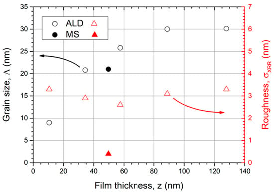
Figure 5.
The estimated grain size by the Scherrer equation (left, ○) increases with coating thickness and saturates at Λ = 30 nm. The roughness evolution with increasing Ru film thickness is additionally shown (right, ∆). The filled symbols correspond to the MS coating.
The estimated grain sizes by the Scherrer equation from XRD are commonly smaller than from SEM images because only coherently scattering areas contribute to the signal. Other effects, e.g., mechanical stress, can also lead to a broadening of Bragg peaks and thus apparently smaller grains. Hence, the Scherrer values are considered as a lower limit value.
In relation, the surface roughness σ of all ALD coatings with thicknesses between 10 and 130 nm show similar results between 2 and 4 nm (AFM measurement). Interestingly, the thinnest layers demonstrate high roughness values that are as high as for thick layers. Due to the nucleation process, we assume the appearance of a Ru film which is not a fully closed layer with protruding crystals. This effect could cause the high roughness at the early observation stage. As the film thickness increases, the layer closes and smooths out the surface to a roughness of only 2.6 nm for a 57 nm thick coating. When the film thickness further increases, the surface roughness rises as well, but no blisters have been observed. This can be explained by larger Ru crystals. Due to the fact that the crystal size growth saturates, we also expect a saturated roughness of coatings with thicknesses larger than z > 150 nm. The MS Ru coating is much smoother, although the crystal size has comparable dimensions (σ = 0.5 nm, Λ = 21 nm) compared to the ALD sample (σ = 2.6 nm, Λ = 26 nm). All investigated coating properties for a 50 nm thick film are summarized and compared with an MS coating in Table 1.

Table 1.
Comparison of coating properties of a 57.5 nm thick ALD and a 50 nm thick MS Ru coating.
3.2. Optical Properties
The measurement of the reflectance in the XUV spectral range requires specialized beamline equipment, which is only available in a few research centers. Hence, the XUV reflectance measurement could be carried out only 5 months after deposition of the ALD samples. Degradation of the Ru ALD samples with time cannot be fully excluded. The thickness of the Ru thin films for XUV applications at a grazing angle of incidence should exceed tens of nanometers to obtain high reflectance values. Further, for numerous reasons, even film thicknesses >200 nm are required to ensure the stability of the mirror optics at the beamline to minimize damage due to the radiation. In Figure 6, the reflection data determined for an ALD sample with a layer thickness of z = 35 nm is compared to a sputtered Ru film (z = 50 nm). A lower reflection appears for the fixed angle of incidence Θ = 10° in the spectral range between λ = 2 nm and 25 nm (Figure 6) for the ALD coating as compared to the MS sample. In addition to the normalized integral reflection, the critical angle for the ALD film is significantly smaller (see Table 2).
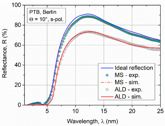
Figure 6.
Comparison of experimental reflection data of sputtered and ALD Ru films in the soft X-ray and extreme UV (XUV) spectral range. Shown in red is the fit with the simulation model Ru + RuO2 + C. In blue, the reflectivity without a surface oxide and ideal smooth interfaces is shown.
Table 2.
Comparison of the optical properties and simulation results for a 35 nm thick ALD and a 50 nm thick sputtered Ru layer from XUV reflectometry (XUVR) measurements.
Although a simple single-layer model leads to a good agreement with the experiment for the XRR simulations, the model had to be improved by two additional layers besides surface roughness to fit the XUV reflectance data. First, a ruthenium(IV) oxide layer (RuO2: ρ = 7.0 g·cm−3) on the Ru surface was assumed, and second carbon residuals (C: ρ = 2.0 g·cm−3). These thin surface layers could not be detected by XRR due to the high surface roughness. The characteristic oscillation is suppressed in XRR even at small angles of incidence. Hence, the features of the thin surface layer, which typically occur at large angles, are not visible.
With the extended model, the XUVR measurement data could be fitted very well. The fit shows that the surface of the ALD coating is significantly rougher (σALD = (4.5 ± 0.6) nm) than that of the sputtered film (σMS = (0.7 ± 0.3) nm). These results are in qualitative agreement with the XRR study of the roughness. The surface roughness is a critical factor affecting the reflectivity at XUV wavelength range because the microstructural relevant size of the surface is close to the wavelength of light. In terms of reflectivity, the higher roughness of the ALD coating leads to a reduction of nearly 20% compared to the MS coating. In the XUVR simulations, the thickness of the surface oxide on the ALD film is larger (doxide = 2.5 nm) compared to the sputtered layer (doxide = 1.0 nm). Due to the increased surface roughness and grainy topography of the ALD sample, it is assumed as the cause of the increased oxide thickness. Furthermore, a 1.6 nm thick C layer was fitted on the RuO2 layer. This third layer was not presumed for the simulation of the sputtered sample. The C residuals on the surface of the ALD layer could be attributed to reaction products during the ALD process because C is a component of the precursor Ru(EtCp)2. Additionally, the C surface contamination due to increased roughness and long storage time is probable.
If the influences of the surface roughness σ and the layer thicknesses (RuO2, C) for the ALD coating are considered separately, σ describes three-quarters of the reflection losses with respect to the normalized integral reflection Rexp. If the reflection curve is simulated with a RuO2 and C layer, it leads to a quarter of the reflection losses, neglecting the surface roughness (σ = 0 nm). This observation shows that the roughness of the Ru ALD film is the critical reflection-reducing effect. The simulation results with the optical properties are summarized in Table 2.
3.3. Chemical Analysis
To verify the XUVR simulation model, XPS and an AES depth profile were performed on a z = 57 nm thick ALD sample. With both methods, only Ru and O were detected. The XPS survey spectra with indicated features are shown in Figure 7. Oxygen is mainly present on the surface because the Ru features decrease stronger than the O features with increasing angle of photoelectron emission (increased surface sensitivity). The Ru 3d3/2 state overlaps the C 1s state at EB ≈ 285 eV (see Figure 7 inset). Unfortunately, a determination of the amount of adventitious C on the surface is not possible because the C 1s peak is obstructed by the Ru 3d3/2 feature.
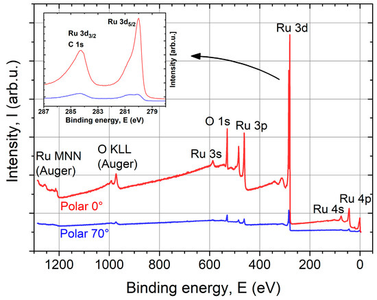
Figure 7.
X-ray photoelectron spectroscopy (XPS) survey spectra of ALD Ru (z = 57 nm) coating on a Si substrate at normal emission (0°) and a polar angle of 70° with indicated features. Only Ru and O were detected, with O mainly being present on the layer surface. The inset shows a zoom-in into the Ru 3d state region.
The Ru 3d5/2 peak appears asymmetric at normal emission (0°) and has clearly two components at 70°. This originates from metallic Ru and oxidized Ru. Based on the binding energies of different Ru oxides, the surface oxide can be confirmed as RuO2 corresponding to the shoulder around 280.8 eV (see Table 3). The thickness of the surface RuO2 layer can be estimated between 1 nm and 2 nm, which is in agreement with the XUVR simulation.
Table 3.
Binding energies of Ru 3d5/2 state for metallic Ru and different Ru oxides [46].
Figure 8 presents an atomic ratios depth profile for Ru and O using AES. On the surface, that means without sputtering, more than 60 at % O is situated which fits to a thin RuO2 on the surface. The O content decreases exponentially with increasing sputter depth and remains at 0.8% in the bulk material. Probably due to the high surface roughness, no ideal layered structure of RuO2 and Ru occurs. Carbon was not measurable, because the Ru signal overlaps spectrally the C signal again.
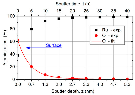
Figure 8.
Atomic ratios depth profile for Ru and O of ALD Ru (z = 57 nm) coating on a Si substrate using Auger electron spectroscopy (AES). The composition on the surface fits RuO2, whereby the O content decreases fast with increasing sputter depth and remains at 0.8% in the bulk material. The sputter depth is a rough approximation, whereby the sputter rate is roughly 8 nm/min.
4. Discussion
Ruthenium thin films deposited by ALD have been thoroughly characterized. The typical ALD temperature window to obtain a constant growth rate for the specific process is in the range of 230 to 300 °C. However, the nucleation and film properties significantly depend on the deposition temperature.
The results obtained in this study indicate that further optimization of ALD Ru coatings for optical applications is essential to leverage on the ALD capability of conformal coatings on nanostructured substrates or on complex shaped optics. The comparison between the ALD and MS technologies has pointed out several advantages of the MS technology. As shown, a sputtered Ru coating resulted in a highly dense and smooth film. The reflection measurements and simulations (Figure 6) indicate that the smooth interfaces are essential for high reflection properties at short wavelengths. The reflectance of the sputtered coatings is approximately 20% higher than the ALD coatings at the peak wavelength of 12 nm. However, there are also disadvantages for MS compared to ALD. The XRD pattern suggests higher film stress in MS films. Stress can lead to deviations of manufacturing tolerances or delamination. Alagoz et al. reported that highly dense Ru films could not be grown to a thickness of higher than 85 nm by magnetron sputtering because they started to peel off beyond this thickness [47]. In this study, Ru coating with a film thickness of 120 nm has been achieved by ALD although it is a relatively slow deposition process. In general, the crystal size and roughness continuously grow with increasing film thickness in MS coatings [48], whereas in ALD the crystal size and surface roughness do not alter with increasing coating thickness. The roughness evolution of MS films, caused by grain growth, increases significantly in thicker coatings in contrast to ALD. The technology of ALD has further advantages compared with conventional MS. A conformal deposition is possible over large areas and even on complex-shaped substrates [49]. Furthermore, there is the possibility to switch easily between Ru and RuO2 coatings while increasing the O2 pressure and pulse lengths [18].
Concerning the optical properties, the higher surface roughness of ALD coatings mainly reduces the reflection at short wavelengths. We tried to reduce the crystal growth to smaller grains and thus the roughness evolution. While Park et al. reported smoother surfaces of σ = 0.9 nm with an NH3 based PEALD process [34], there was no improvement observed using O2 plasma. No film growth was observed by PEALD with O2 plasma. The O2 plasma was strong enough to instantaneously remove the grown Ru layer. Similar etching phenomena were reported by Belau et al. [20]. Even by changing the deposition temperature, a further improvement of the surface roughness was not possible, and a deposition with NH3 is currently not available in our laboratories.
As potential option to improve the nucleation seed density and thus the fast formation of the first fully closed metal layer, a metal-based seed layer can be implemented as Lu et al. reported that no nucleation delay was found on Pt and Pd layers [5]. Furthermore, Kim et al. showed a nucleation improvement and a surface roughness reduction by O3 supply [10]. An alternative chemistry of precursor and co-reactant is also possible. There are several other precursors and processes that achieved smoother Ru ALD films, e.g., Ru(MePy)2: σ = 0.2 nm [50], RuEtPy: σ = 0.4 nm [51] and RuO4 with H2: σ = 0.3 nm. However, with regard to other necessary requirements for optical applications, e.g., high purity and high density, these processes need to be evaluated in detail.
The chemical analysis of the ALD Ru surface has confirmed the presence of a thin oxide layer at the surface of the coating; however, not within the film. This ultra-thin surface layer also significantly affects the XUV reflection of the ALD Ru, even though not as much as the high surface roughness. The oxide layer might be related to the chemical process which involves an oxidizing step to remove the organic ligands of the Ru(EtCp)2 precursor. In the O2 pulse step, the Ru would be also partially oxidized. In the following metalorganic pulse, the oxide is probably decomposed and the precursor ligands serve as a reducing agent. Hence, little oxygen contamination is being detected in the film. In contrast, at the surface, the reaction terminates with the O2 pulse and remaining RuO2 is not further reduced. This further motivates the development of oxygen free ALD processes of metals.
5. Conclusions
Ruthenium thin films grown by ALD have been evaluated for optical applications. High-density Ru films have successfully been deposited on Si and fused silica substrates. Temperatures above 230 °C are required for a film formation using Ru(EtCp)2 and O2. Higher deposition temperatures above 275 °C have led to blisters that increased the surface roughness significantly and reduced the adhesion properties. With an optimized deposition temperature of 250 °C, we have explored the film growth and the resulting optical properties. The polycrystalline growth and the corresponding evolution of the surface roughness have led to major reflection losses at short wavelengths. Sputtered Ru coatings show similar density but are much smoother than ALD coatings. The ALD samples show a thin (<2 nm) RuO2 surface layer and 0.8 at % residual O in bulk material. Carbon impurities were not measurable. Further experimental development is required to leverage on the major benefit of ALD to realize conformal coatings on complex-shaped substrates towards coatings with high reflectance and stability for optical applications.
Author Contributions
Conceptualization, R.M., L.G., and A.S.; ALD Depositions, L.G.; SEM Characterization, S.W.; AFM Measurements, V.B., XRR and XUV Analysis, R.M.; XPS and AES Analysis, F.O. and T.F.; Writing–Original Draft Preparation, R.M. and P.S.; Writing–Review and Editing, P.S., L.G., T.F, and A.S.; Supervision, A.S.; Project Administration, A.S., N.K. and A.T.; Funding Acquisition, A.S., N.K. and A.T.
Funding
This research was funded by the Fraunhofer Society Attract Project (No. 066-601020), the Fraunhofer IOF, Center of Excellence in Photonics and the Deutsche Forschungsgemeinschaft (DFG) Emmy-Noether-Project (No. SZ235/1-1).
Acknowledgments
The authors thank David Kästner for the technical support and Philipp Naujok for helpful discussions. We also acknowledge constructive comments of reviewers to improve the article.
Conflicts of Interest
The authors declare no conflict of interest. The funders had no role in the design of the study; in the collection, analyses, or interpretation of data; in the writing of the manuscript, or in the decision to publish the results.
References
- Yeo, S.; Choi, S.-H.; Park, J.-Y.; Kim, S.-H.; Cheon, T.; Lim, B.-Y.; Kim, S. Atomic layer deposition of ruthenium (Ru) thin films using ethylbenzen-cyclohexadiene Ru (0) as a seed layer for copper metallization. Thin Solid Films 2013, 546, 2–8. [Google Scholar] [CrossRef]
- Minjauw, M.M.; Dendooven, J.; Capon, B.; Schaekers, M.; Detavernier, C. Near room temperature plasma enhanced atomic layer deposition of ruthenium using the RuO4-precursor and H2-plasma. J. Mater. Chem. C 2015, 3, 4848–4851. [Google Scholar] [CrossRef]
- Bajt, S.; Dai, Z.R.; Nelson, E.J.; Wall, M.A.; Alameda, J.; Nguyen, N.; Baker, S.; Robinson, J.C.; Taylor, J.S.; Clift, M.; et al. Oxidation resistance of Ru-capped EUV multilayers. Proc. SPIE 2005, 5751, 118–127. [Google Scholar] [CrossRef]
- Aoyama, T.; Eguchi, K. Ruthenium films prepared by liquid source chemical vapor deposition using bis-(ethylcyclopentadienyl)ruthenium. Jpn. J. Appl. Phys. 1999, 38, L1134. [Google Scholar] [CrossRef]
- Lu, J.; Elam, J.W. Low temperature ABC-type Ru atomic layer deposition through consecutive dissociative chemisorption, combustion, and reduction steps. Chem. Mater. 2015, 27, 4950–4956. [Google Scholar] [CrossRef]
- Aaltonen, T.; Alén, P.; Ritala, M.; Leskelä, M. Ruthenium thin films grown by atomic layer deposition. Chem. Vap. Depos. 2003, 9, 45–49. [Google Scholar] [CrossRef]
- Lee, J.; Song, Y.W.; Lee, K.; Lee, Y.; Jang, H.K. Atomic layer deposition of Ru by using a new Ru-precursor. ECS Trans. 2006, 2, 1–11. [Google Scholar] [CrossRef]
- Misra, V.; Lucovsky, G.; Parsons, G. Issues in high-K gate stack interfaces. MRS Bull. 2002, 27, 212–216. [Google Scholar] [CrossRef]
- Leick-Marius, N. Atomic layer deposition of ruthenium films: Properties and surface reactions. Ph.D. Thesis, Technische Universiteit Eindhoven, Eindhoven, The Netherlands, 2014. [Google Scholar]
- Kim, J.-Y.; Kil, D.-S.; Kim, J.-H.; Kwon, S.-H.; Ahn, J.-H.; Roh, J.-S.; Park, S.-K. Ru films from bis(ethylcyclopentadienyl)ruthenium using ozone as a reactant by atomic layer deposition for capacitor electrodes. J. Electrochem. Soc. 2012, 159, H560–H564. [Google Scholar] [CrossRef]
- Marczuk, P.; Egle, W. Source collection optics for EUV lithography. In Advances in Mirror Technology for X-ray, EUV Lithography, Laser, and Other Applications II; Khounsary, A.M., Dinger, U., Ota, K., Eds.; SPIE Optical Engineering: Bellingham, WA, USA, 2004; Volume 5533, pp. 145–157. [Google Scholar]
- Weber, T.; Käsebier, T.; Szeghalmi, A.; Knez, M.; Kley, E.-B.; Tünnermann, A. Iridium wire grid polarizer fabricated using atomic layer deposition. Nanoscale Res. Lett. 2011, 6, 558. [Google Scholar] [CrossRef] [PubMed]
- Weber, T.; Käsebier, T.; Szeghalmi, A.; Knez, M.; Kley, E.-B.; Tünnermann, A. High aspect ratio deep UV wire grid polarizer fabricated by double patterning. Microelectron. Eng. 2012, 98, 433–435. [Google Scholar] [CrossRef]
- Jefimovs, K.; Vila-Comamala, J.; Pilvi, T.; Raabe, J.; Ritala, M.; David, C. Zone-doubling technique to produce ultrahigh-resolution X-ray optics. Phys. Rev. Lett. 2007, 99, 264801. [Google Scholar] [CrossRef] [PubMed]
- Shibutami, T.; Kawano, K.; Oshima, N.; Yokoyama, S.; Funakubo, H. A novel ruthenium precursor for MOCVD without seed ruthenium layer. MRS Proc. 2002, 748, U12.7. [Google Scholar] [CrossRef]
- Wang, H.; Gordon, R.G.; Alvis, R.; Ulfig, R.M. Atomic layer deposition of ruthenium thin films from an amidinate precursor. Chem. Vap. Depos. 2009, 15, 312–319. [Google Scholar] [CrossRef]
- Minjauw, M.M.; Dendooven, J.; Capon, B.; Schaekers, M.; Detavernier, C. Atomic layer deposition of ruthenium at 100 °C using the RuO4-precursor and H2. J. Mater. Chem. C 2015, 3, 132–137. [Google Scholar] [CrossRef]
- Methaapanon, R.; Geyer, S.M.; Lee, H.-B.-R.; Bent, S.F. The low temperature atomic layer deposition of ruthenium and the effect of oxygen exposure. J. Mater. Chem. 2012, 22, 25154–25160. [Google Scholar] [CrossRef]
- Kwon, O.-K.; Kwon, S.-H.; Park, H.-S.; Kang, S.-W. PEALD of a Ru adhesion layer for Cu interconnects. J. Electrochem. Soc. 2004, 151, C753–C756. [Google Scholar] [CrossRef]
- Belau, L.; Park, J.Y.; Liang, T.; Somorjai, G.A. The effects of oxygen plasma on the chemical composition and morphology of the Ru capping layer of the extreme ultraviolet mask blanks. J. Vac. Sci. Technol. B 2008, 26, 2225–2229. [Google Scholar] [CrossRef]
- Hill, S.B.; Ermanoski, I.; Tarrio, C.; Lucatorto, T.B.; Madey, T.E.; Bajt, S.; Fang, M.; Chandhok, M. Critical parameters influencing the EUV-induced damage of Ru-capped multilayer mirrors. Proc. SPIE 2007, 6517. [Google Scholar] [CrossRef]
- Nieto, M.; Allain, J.-P.; Titov, V.; Hendricks, M.R.; Hassanein, A.; Rokusek, D.; Chrobak, C.; Tarrio, C.; Barad, Y.; Grantham, S.; et al. Effect of xenon bombardment on ruthenium-coated grazing incidence collector mirror lifetime for extreme ultraviolet lithography. J. Appl. Phys. 2006, 100, 053510. [Google Scholar] [CrossRef]
- Shin, H.; Sporre, J.R.; Raju, R.; Ruzic, D.N. Reflectivity degradation of grazing-incident EUV mirrors by EUV exposure and carbon contamination. Microelectron. Eng. 2009, 86, 99–105. [Google Scholar] [CrossRef]
- Zocchi, F.E.; Benedetti, E. Optical designs of grazing incidence collector for extreme ultraviolet lithography. J. Micro/Nanolithogr. MEMS MOEMS 2007, 6, 043002. [Google Scholar] [CrossRef]
- Sweatt, W.C.; Kubiak, G.D. Condenser for Extreme-UV Lithography with Discharge Source. U.S. Patent 6,285,737 B1, 4 September 2001. [Google Scholar]
- Kwon, O.-K.; Kim, J.-H.; Park, H.-S.; Kang, S.-W. Atomic layer deposition of ruthenium thin films for copper glue layer. J. Electrochem. Soc. 2004, 151, G109–G112. [Google Scholar] [CrossRef]
- Sergey, Y. Multilayer Coatings for EUV/Soft X-ray Mirrors. In Optical Interference Coatings; Kaiser, N., Pulker, H.K., Eds.; Springer: Berlin, Germany, 2003; p. 299. [Google Scholar]
- LEPTOS 7.8 (2014). Available online: https://www.bruker.com/products/x-ray-diffraction-and-elemental-analysis/x-ray-diffraction/xrd-software/leptos/leptos-r.html (accessed on 10 November 2018).
- Scherrer, P. Bestimmung der Größe und der inneren Struktur von Kolloidteilchen mittels Röntgenstrahlen. In Kolloidchemie Ein Lehrbuch. Chemische Technologie in Einzeldarstellungen; Springer: Berlin/Heidelberg, Germany, 1912; pp. 387–409. [Google Scholar]
- Scholze, F.; Tümmler, J.; Ulm, G. High-accuracy radiometry in the EUV range at the PTB soft x-ray beamline. Metrologia 2003, 40, S224. [Google Scholar] [CrossRef]
- Windt, D.L. IMD-Software for modeling the optical properties of multilayer films. Comput. Phys. 1998, 12, 360–370. [Google Scholar] [CrossRef]
- Henke, B.L.; Gullikson, E.M.; Davis, J.C. X-ray interactions: Photoabsorption, scattering, transmission, and reflection at E = 50–30,000 eV, Z = 1–92. Atomic Data Nucl. Data Tables 1993, 54, 181–342. [Google Scholar] [CrossRef]
- Hämäläinen, J.; Ritala, M.; Leskelä, M. Atomic layer deposition of noble metals and their oxides. Chem. Mater. 2014, 26, 786–801. [Google Scholar] [CrossRef]
- Park, S.-J.; Kim, W.-H.; Lee, H.-B.-R.; Maeng, W.J.; Kim, H. Thermal and plasma enhanced atomic layer deposition ruthenium and electrical characterization as a metal electrode. Microelectron. Eng. 2008, 85, 39–44. [Google Scholar] [CrossRef]
- Aaltonen, T.; Ritala, M.; Arstila, K.; Keinonen, J.; Leskelä, M. Atomic layer deposition of ruthenium thin films from Ru(thd)3 and oxygen. Chem. Vap. Depos. 2004, 10, 215–219. [Google Scholar] [CrossRef]
- Kukli, K.; Kemell, M.; Puukilainen, E.; Aarik, J.; Aidla, A.; Sajavaara, T.; Laitinen, M.; Tallarida, M.; Sundqvist, J.; Ritala, M.; et al. Atomic layer deposition of ruthenium films from (ethylcyclopentadienyl)(pyrrolyl)ruthenium and oxygen. J. Electrochem. Soc. 2011, 158, D158. [Google Scholar] [CrossRef]
- Aaltonen, T.; Rahtu, A.; Ritala, M.; Leskelä, M. Reaction mechanism studies on atomic layer deposition of ruthenium and platinum. Electrochem. Solid State Lett. 2003, 6, C130. [Google Scholar] [CrossRef]
- Perry, D.L. Handbook of Inorganic Compounds; CRC Press: Boca Raton, FL, USA, 2011. [Google Scholar]
- Wojcik, H.; Junige, M.; Bartha, W.; Albert, M.; Neumann, V.; Merkel, U.; Peeva, A.; Gluch, J.; Menzel, S.; Munnik, F.; et al. Physical characterization of PECVD and PEALD Ru(-C) films and comparison with PVD ruthenium film properties. J. Electrochem. Soc. 2012, 159, H166–H176. [Google Scholar] [CrossRef]
- George, S.M. Atomic layer deposition: An overview. Chem. Rev. 2010, 110, 111–131. [Google Scholar] [CrossRef] [PubMed]
- Spiller, E.A. Soft X-ray Optics; SPIE Optical Engineering: Bellingham, WA, USA, 1994; p. 235. [Google Scholar]
- Manke, C.; Miedl, S.; Boissiere, O.; Baumann, P.K.; Lindner, J.; Schumacher, M.; Brodyanski, A.; Scheib, M. Atomic vapor deposition of Ru and RuO2 thin film layers for electrode applications. Microelectron. Eng. 2005, 82, 242–247. [Google Scholar] [CrossRef]
- Genevée, P.; Ahiavi, E.; Janunts, N.; Pertsch, T.; Oliva, M.; Kley, E.-B.; Szeghalmi, A. Blistering during the atomic layer deposition of iridium. J. Vac. Sci. Technol. A 2016, 34, 01A113. [Google Scholar] [CrossRef]
- Gadkari, P.R.; Warren, A.P.; Todi, R.M.; Petrova, R.V.; Coffey, K.R. Comparison of the agglomeration behavior of thin metallic films on SiO2. J. Vac. Sci. Technol. A 2005, 23, 1152–1161. [Google Scholar] [CrossRef]
- Powder Diffraction File; Pattern 06-0663; ICDD: Newtown Square, PA, USA, 1997.
- Moulder, J.F.; Stickle, W.F.; Sobol, P.E.; Bomben, K.D. Handbook of X-ray Photoelectron Spectroscopy; Physical Electronics, Inc.: Eden Prairie, MN, USA, 2009; pp. 114–115. [Google Scholar]
- Alagoz, A.S.; Kamminga, J.-D.; Grachev, S.Y.; Lu, T.-M.; Karabacak, T. Residual stress reduction in sputter deposited thin films by density modulation. MRS Proc. 2009, 1224, 1224-FF05-22. [Google Scholar] [CrossRef]
- Petrov, I.; Barna, P.B.; Hultman, L.; Greene, J.E. Microstructural evolution during film growth. J. Vac. Sci. Technol. A 2003, 21, S117–S128. [Google Scholar] [CrossRef]
- Pfeiffer, K.; Schulz, U.; Tünnermann, A.; Szeghalmi, A. Antireflection Coatings for Strongly Curved Glass Lenses by Atomic Layer Deposition. Coatings 2017, 7, 118. [Google Scholar] [CrossRef]
- Kukli, K.; Aarik, J.; Aidla, A.; Jõgi, I.; Arroval, T.; Lu, J.; Sajavaara, T.; Laitinen, M.; Kiisler, A.-A.; Ritala, M.; et al. Atomic layer deposition of Ru films from bis(2,5-dimethylpyrrolyl)ruthenium and oxygen. Thin Solid Films 2012, 520, 2756–2763. [Google Scholar] [CrossRef]
- Geidel, M.; Junige, M.; Albert, M.; Bartha, J.W. In-situ analysis on the initial growth of ultra-thin ruthenium films with atomic layer deposition. Microelectron. Eng. 2013, 107, 151–155. [Google Scholar] [CrossRef]


© 2018 by the authors. Licensee MDPI, Basel, Switzerland. This article is an open access article distributed under the terms and conditions of the Creative Commons Attribution (CC BY) license (http://creativecommons.org/licenses/by/4.0/).