Growth without Postannealing of Monoclinic VO2 Thin Film by Atomic Layer Deposition Using VCl4 as Precursor


Abstract
1. Introduction
2. Materials and Methods
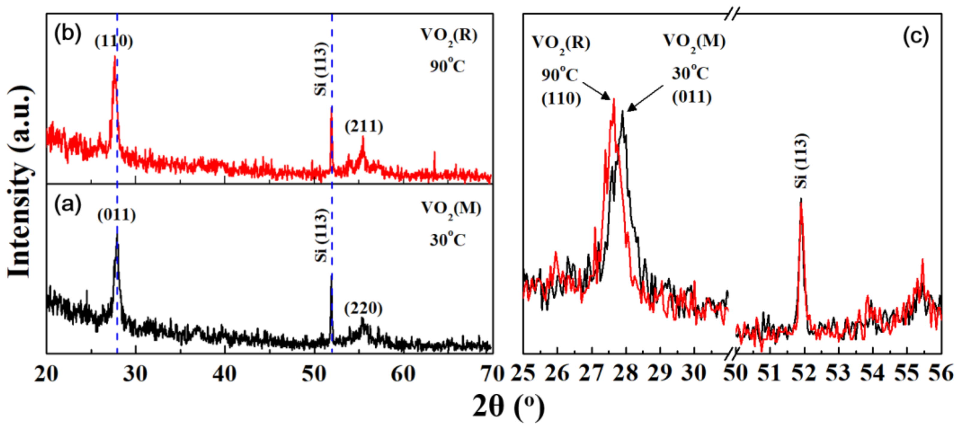
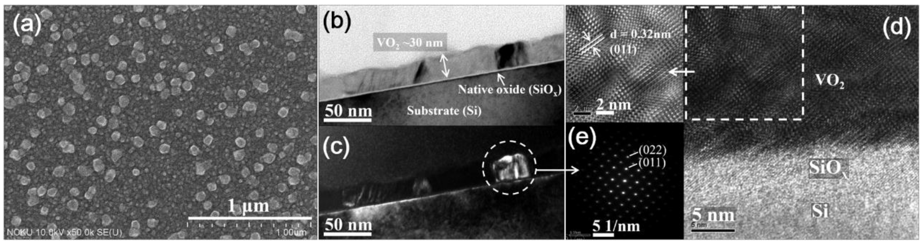
3. Results and Discussion
4. Conclusions
Supplementary Materials
Funding
Acknowledgment
Conflicts of Interest
References
- Morin, F.J. Oxides which show a metal-to-insulator transition at the Neel temperature. Phys. Rev. Lett. 1959, 3, 34–36. [Google Scholar] [CrossRef]
- Barker, A.S.; Verleur, H.W.; Guggenheim, H.J. Infrared optical properties of vanadium dioxide above and below the transition temperature. Phys. Rev. Lett. 1966, 17, 1286–1289. [Google Scholar] [CrossRef]
- Park, J.H.; Coy, J.M.; Kasirga, T.S.; Huang, C.; Fei, Z.; Hunter, S.; Cobdem, D.H. Measurement of a solid-state triple point at the metal-insulator transition in VO2. Nature 2013, 500, 431–434. [Google Scholar] [CrossRef] [PubMed]
- O’Callahan, B.T.; Jones, A.C.; Park, J.H.; Cobden, D.H.; Atkin, J.M.; Raschke, M.B. Inhomogeneity of the ultrafast insulator-to-metal transition dynamics of VO2. Nat. Commun. 2015, 6, 6849. [Google Scholar] [CrossRef] [PubMed]
- Cueff, S.; Li, D.; Zhou, Y.; Wong, F.J.; Kurvits, J.A.; Ramanathan, S.; Zia, R. Dynamic control of light emission faster than the lifetime limit using VO2 phase-change. Nat. Commun. 2015, 6, 8636. [Google Scholar] [CrossRef] [PubMed]
- Yang, Z.; Ko, C.; Ramanathan, S. Oxide electronics utilizing ultrafast metal-insulator transitions. Annu. Rev. Mater. Res. 2011, 41, 337–367. [Google Scholar] [CrossRef]
- Nakano, M.; Shibuya, K.; Okuyama, D.; Hatano, T.; Ono, S.; Kawasaki, M.; Iwasa, Y.; Tokura, Y. Collective bulk carrier delocalization driven by electrostatic surface charge accumulation. Nature 2012, 487, 459–462. [Google Scholar] [CrossRef] [PubMed]
- Wang, N.; Liu, S.; Zeng, X.T.; Magdassi, S.; Long, Y. Mg/W-codoped vanadium dioxide thin films with enhanced visible transmittance and low phase transition temperature. J. Mater. Chem. C 2015, 3, 6771–6777. [Google Scholar] [CrossRef]
- Zhang, S.; Kim, I.S.; Lauhon, L.J. Stoichiometry engineering of monoclinic to rutile phase transition in suspended single crystalline vanadium dioxide nanobeams. Nano Lett. 2011, 11, 1443–1447. [Google Scholar] [CrossRef] [PubMed]
- Petraru, A.; Soni, R.; Kohlstedt, H. Voltage controlled biaxial strain in VO2 films grown on 0.72Pb(Mg1/3Nb2/3)-0.28PbTiO3 crystals and its effect on the transition temperature. Appl. Phys. Lett. 2014, 105, 092902. [Google Scholar] [CrossRef]
- Jian, J.; Chen, A.; Zhang, W.; Wang, H. Sharp semiconductor-to-metal transition of VO2 thin films on glass substrates. J. Appl. Phys. 2013, 114, 244301. [Google Scholar] [CrossRef]
- Jeong, J.; Aetukuri, N.; Graf, T.; Schladt, T.D.; Samant, M.G.; Parkin, S.S.P. Suppression of metal-insulator transition in VO2 by electric field-induced oxygen vacancy formation. Science 2013, 339, 1402–1405. [Google Scholar] [CrossRef] [PubMed]
- Aetukuri, N.B.; Gary, A.X.; Drouard, M.; Cossale, M.; Gao, L.; Reid, A.H.; Kukreja, R.; Ohldag, H.; Jenkins, C.A.; Arenholz, E.; et al. Control of the metal–insulator transition in vanadium dioxide by modifying orbital occupancy. Nat. Phys. 2013, 9, 661–666. [Google Scholar] [CrossRef]
- Wu, J.M.; Liou, L.B. Room temperature photo-induced phase transitions of VO2 nanodevices. J. Mater. Chem. 2011, 21, 5499–5504. [Google Scholar] [CrossRef]
- Xu, F.; Cao, X.; Luo, H.; Jin, P. Recent advances in VO2-based thermochromic composites for smart windows. J. Mater. Chem. C 2018, 6, 1903–1919. [Google Scholar] [CrossRef]
- Shukla, N.; Parihar, A.; Freeman, E.; Paik, H.; Stone, G.; Narayanan, V.; Wen, H.; Cai, Z.; Gopalan, V.; Engel-Herbert, R.; et al. Synchronized charge oscillations in correlated electron systems. Sci. Rep. 2014, 4, 4964. [Google Scholar] [CrossRef]
- Ruzmetov, D.; Gopalakrishnan, G.; Ko, C.; Narayanamurti, V.; Ramanathan, S. Three-terminal field effect devices utilizing thin film vanadium oxide as the channel layer. J. Appl. Phys. 2010, 107, 114516. [Google Scholar] [CrossRef]
- Yajima, T.; Nishimura, T.; Toriumi, A. Positive-bias gate-controlled metal–insulator transition in ultrathin VO2 channels with TiO2 gate dielectrics. Nat. Commun. 2015, 6, 10104. [Google Scholar] [CrossRef] [PubMed]
- Briggs, R.M.; Pryce, I.M.; Atwater, H.A. Compact silicon photonic waveguide modulator based on the vanadium dioxide metal-insulator phase transition. Opt. Express 2010, 18, 11192–11201. [Google Scholar] [CrossRef] [PubMed]
- Gu, Q.; Falk, A.; Wu, J.Q.; Ouyang, L.; Park, H. Current-driven phase oscillation and domain-wall propagation in WxV1-xO2 nanobeams. Nano Lett. 2007, 7, 363–366. [Google Scholar] [CrossRef] [PubMed]
- Dicken, M.J.; Aydin, K.; Pryce, I.M.; Sweatlock, L.A.; Boyd, E.M.; Walavalkar, S.; Ma, J.; Atwater, H.A. Frequency tunable near-infrared metamaterials based on VO2 phase transition. Opt. Express 2009, 17, 18330–18339. [Google Scholar] [CrossRef] [PubMed]
- Driscoll, T.; Kim, H.T.; Chae, B.G.; Di Ventra, M.; Basov, D.N. Phase-transition driven memristive system. Appl. Phys. Lett. 2009, 95, 043503. [Google Scholar] [CrossRef]
- Kim, B.J.; Lee, Y.W.; Chae, B.G.; Yun, S.J.; Oh, S.Y.; Kim, H.T. Temperature dependence of the first-order metal-insulator transition in VO2 and programmable critical temperature sensor. Appl. Phys. Lett. 2007, 90, 023515. [Google Scholar] [CrossRef]
- Strelcov, E.; Lilach, Y.; Kolmakov, A. Gas sensor based on metal-insulator transition in VO2 nanowire thermistor. Nano Lett. 2009, 9, 2322–2326. [Google Scholar] [CrossRef] [PubMed]
- Heckman, E.M.; Gonzalez, L.P.; Guha, S.; Barnes, J.O.; Carpenter, A. Electrical and optical switching properties of ion implanted VO2 thin films. Thin Solid Films 2009, 518, 265–268. [Google Scholar] [CrossRef]
- Ureña-Begara, F.; Crunteanu, A.; Raskin, J.P. Raman and XPS characterization of vanadium oxide thin films with temperature. Appl. Surf. Sci. 2017, 403, 717–727. [Google Scholar] [CrossRef]
- Chiu, T.W.; Tonooka, K.; Kikuchi, N. Growth of b-axis oriented VO2 thin films on glass substrates using ZnO buffer layer. Appl. Surf. Sci. 2010, 256, 6834–6837. [Google Scholar] [CrossRef]
- Zhang, P.; Jiang, K.; Deng, Q.; You, Q.; Zhang, J.; Wu, J.; Hu, Z.; Chu, J. Manipulations from oxygen partial pressure on the higher energy electronic transition and dielectric function of VO2 films during a metal-insulator transition process. J. Mater. Chem. C 2015, 3, 5033–5040. [Google Scholar] [CrossRef]
- Zhang, H.T.; Zhang, L.; Mukherjee, D.; Zheng, Y.X.; Haislmaier, R.C.; Alem, N.; Engel-Herbert, R. Wafer-scale growth of VO2 thin films using a combinatorial approach. Nat. Commun. 2015, 6, 8475. [Google Scholar] [CrossRef] [PubMed]
- Vernardou, D.; Pemble, M.E.; Sheel, D.W. The growth of thermochromic VO2 films on glass by atmospheric-pressure CVD: A comparative study of precursors, CVD methodology, and substrates. Chem. Vap. Depos. 2006, 12, 263–274. [Google Scholar] [CrossRef]
- Vernardou, D.; Paterakis, P.; Drosos, H.; Spanakis, E.; Povey, I.M.; Pemble, M.E.; Koudoumas, E.; Katsarakis, N. A study of the electrochemical performance of vanadium oxide thin films grown by atmospheric pressure chemical vapour deposition. Sol. Energy Mater. Sol. Cells 2011, 95, 2842–2847. [Google Scholar] [CrossRef]
- Vernardou, D. Using an atmospheric pressure chemical vapor deposition process for the development of V2O5 as an electrochromic material. Coatings 2017, 7, 24. [Google Scholar] [CrossRef]
- Makarevich, A.M.; Sadykov, I.I.; Sharovarov, D.I.; Amelichev, V.A.; Adamenkov, A.A.; Tsymbarenko, D.M.; Plokhih, A.V.; Esaulkov, M.N.; Solyankin, P.M.; Kaul, A.R. Chemical synthesis of high quality epitaxial vanadium dioxide films with sharp electrical and optical switch properties. J. Mater. Chem. C 2015, 3, 9197–9205. [Google Scholar] [CrossRef]
- Blackburn, B.; Powell, M.J.; Knapp, C.E.; Bear, J.C.; Carmalt, C.J.; Parkin, I.P. [{VOCl2(CH2(COOEt)2)}4] as a molecular precursor for thermochromic monoclinic VO2 thin films and nanoparticles. J. Mater. Chem. C 2016, 4, 10453–10463. [Google Scholar] [CrossRef]
- Rampelberg, G.; Schaekers, M.; Martens, K.; Xie, Q.; Deduytsche, D.; De Schutter, B.; Blasco, N.; Kittl, J.; Detavernier, C. Semiconductor-metal transition in thin VO2 films grown by ozone based atomic layer deposition. Appl. Phys. Lett. 2011, 98, 162902. [Google Scholar] [CrossRef]
- Premkumar, P.A.; Toeller, M.; Radu, I.P.; Adelmann, C.; Schaekers, M.; Meersschaut, J.; Conard, T.; Elshocht, S.V. Process study and characterization of VO2 thin films synthesized by ALD using TEMAV and O3 precursors. ECS J. Solid State Sci. Technol. 2012, 1, P169–P174. [Google Scholar] [CrossRef]
- Tangirala, M.; Zhang, K.; Nminibapiel, D.; Pallem, V.; Dussarrat, C.; Cao, W.; Adam, T.N.; Johnson, C.S.; Elsayed-Ali, H.E.; Baumgart, H. Physical analysis of VO2 films grown by atomic layer deposition and RF magnetron sputtering. ECS J. Solid State Sci. Technol. 2014, 3, N89–N94. [Google Scholar] [CrossRef]
- Cerbu, F.; Chou, H.S.; Radu, I.P.; Martens, K.; Peter, A.P.; Afanas’ev, V.V.; Stesmans, A. Band alignment and effective work function of atomic-layer deposited VO2 and V2O5 films on SiO2 and Al2O3. Phys. Status Solidi C 2015, 12, 238–241. [Google Scholar] [CrossRef]
- Zhang, K.; Tangirala, M.; Nminibapiel, D.; Cao, W.; Pallem, V.; Dussarrat, C.; Baumgart, H. Synthesis of VO2 thin films by atomic layer deposition with TEMAV as precursor. ECS Trans. 2013, 50, 175–182. [Google Scholar] [CrossRef]
- Blanquart, T.; Niinistö, J.; Gavagnin, M.; Longo, V.; Heikkilä, M.; Puukilainen, E.; Pallem, V.R.; Dussarrat, C.; Ritala, M.; Leskelä, M. Atomic layer deposition and characterization of vanadium oxide thin films. RSC Adv. 2013, 3, 1179–1185. [Google Scholar] [CrossRef]
- Kozen, A.C.; Joress, H.; Currie, M.; Anderson, V.R.; Eddy, C.R., Jr.; Wheeler, V.D. Structural characterization of atomic layer deposited vanadium dioxide. J. Phys. Chem. C 2017, 121, 19341–19347. [Google Scholar] [CrossRef]
- Park, H.H.; Larrabee, T.J.; Ruppalt, L.B.; Culbertson, J.C.; Prokes, S.M. Tunable electrical properties of vanadium oxide by hydrogen-plasma-treated atomic layer deposition. ACS Omega 2017, 2, 1259–1264. [Google Scholar] [CrossRef]
- Musschoot, J.; Deduytsche, D.; Poelman, H.; Haemers, J.; Van Meirhaeghe, R.L.; Van den Berghe, S.; Detavernier, C. Comparison of thermal and plasma-enhanced ALD/CVD of vanadium pentoxide. J. Electrochem. Soc. 2009, 156, P122–P126. [Google Scholar] [CrossRef]
- Boukhalfa, S.; Evanoff, K.; Yushin, G. Atomic layer deposition of vanadium oxide on carbon nanotubes for high-power supercapacitor electrodes. Energy Environ. Sci. 2012, 5, 6872–6879. [Google Scholar] [CrossRef]
- Singh, T.; Wang, S.; Aslam, N.; Zhang, H.; Hoffmann-Eifert, S.; Mathur, S. Atomic layer deposition of transparent VOx thin films for resistive switching applications. Chem. Vap. Depos. 2014, 20, 291–297. [Google Scholar] [CrossRef]
- Daubert, J.S.; Lewis, N.P.; Gotsch, H.N.; Mundy, J.Z.; Monroe, D.N.; Dickey, E.C.; Losego, M.D.; Parsons, G.N. Effect of meso- and micro-porosity in carbon electrodes on atomic layer deposition of pseudocapacitive V2O5 for high performance supercapacitors. Chem. Mater. 2015, 27, 6524–6534. [Google Scholar] [CrossRef]
- Baddour-Hadjean, R.; Golabkan, V.; Pereira-Ramos, J.P.; Mantoux, A.; Lincot, D. A Raman study of the lithium insertion process in vanadium pentoxide thin films deposited by atomic layer deposition. J. Raman Spectrosc. 2002, 33, 631–638. [Google Scholar] [CrossRef]
- Badot, J.C.; Mantoux, A.; Baffier, N.; Dubrunfaut, O.; Lincot, D. Electrical properties of V2O5 thin films obtained by atomic layer deposition (ALD). J. Mater. Chem. 2004, 14, 3411–3415. [Google Scholar] [CrossRef]
- Chen, X.; Pomerantseva, E.; Banerjee, P.; Gregorczyk, K.; Ghodssi, R.; Rubloff, G. Ozone-based atomic layer deposition of crystalline V2O5 films for high performance electrochemical energy storage. Chem. Mater. 2012, 24, 1255–1261. [Google Scholar] [CrossRef]
- Badot, J.C.; Ribes, S.; Yousfi, E.B.; Vivier, V.; Pereira-Ramos, J.P.; Baffier, N.; Lincot, D. Atomic layer epitaxy of vanadium oxide thin films and electrochemical behavior in presence of lithium ions. Electrochem. Solid-State Lett. 2000, 3, 485–488. [Google Scholar] [CrossRef]
- Kim, H.; Maeng, W.J. Applications of atomic layer deposition to nanofabrication and emerging nanodevices. Thin Solid Films 2009, 517, 2563–2580. [Google Scholar] [CrossRef]
- George, S.M. Atomic layer deposition: An overview. Chem. Rev. 2010, 110, 111–131. [Google Scholar] [CrossRef] [PubMed]
- Gelde, L.; Cuevas, A.L.; Martínez de Yuso, M.D.V.; Benavente, J.; Vega, V.; Gonzalez, A.S.; Prida, V.M.; Hernando, B. Influence of TiO2-coating layer on nanoporous alumina membranes by ALD technique. Coatings 2018, 8, 60. [Google Scholar] [CrossRef]
- Cheng, H.E.; Lee, W.J. Properties of TiN films grown by atomic-layer chemical vapor deposition with a modified gaseous-pulse sequence. Mater. Chem. Phys. 2006, 97, 315–320. [Google Scholar] [CrossRef]
- Lee, W.J.; Hon, M.H. Space-limited crystal growth mechanism of TiO2 films by atomic layer deposition. J. Phys. Chem. C 2010, 114, 6917–6921. [Google Scholar] [CrossRef]
- Wu, C.; Zhang, X.; Dai, J.; Yang, J.; Wu, Z.; Wei, S.; Xie, Y. Direct hydrothermal synthesis of monoclinic VO2(M) single-domain nanorods on large scale displaying magnetocaloric effect. J. Mater. Chem. 2011, 21, 4509–4517. [Google Scholar] [CrossRef]
- Silversmit, G.; Depla, D.; Poelman, H.; Martin, G.B.; De Gryse, R. Determination of the V2p XPS binding energies for different vanadium oxidation states (V5+ to V0+). J. Electron. Spectrosc. Relat. Phenom. 2004, 135, 167–175. [Google Scholar] [CrossRef]
- Hryha, E.; Rutqvist, E.; Nyborg, L. Stoichiometric vanadium oxides studied by XPS. Surf. Interface Anal. 2012, 44, 1022–1025. [Google Scholar] [CrossRef]
- Yuan, X.; Zhang, W.; Zhang, P. Hole-lattice coupling and photoinduced insulator-metal transition in VO2. Phys. Rev. B 2013, 88, 035119. [Google Scholar] [CrossRef]
- Zaghrioui, M.; Sakai, J.; Azhan, N.H.; Su, K.; Okimura, K. Polarized Raman scattering of large crystalline domains in VO2 films on sapphire. Vib. Spectrosc. 2015, 80, 79–85. [Google Scholar] [CrossRef]
- Shibuya, K.; Sawa, A. Polarized Raman scattering of epitaxial vanadium dioxide films with low-temperature monoclinic phase. J. Appl. Phys. 2017, 122, 015307. [Google Scholar] [CrossRef]


| Elemental Content | Before Surface Etching | After Surface Etching |
|---|---|---|
| V (at.%) | 25.7 | 33.1 |
| O (at.%) | 74.3 | 66.9 |
| Cl (at.%) | <0.1 | <0.1 |
© 2018 by the authors. Licensee MDPI, Basel, Switzerland. This article is an open access article distributed under the terms and conditions of the Creative Commons Attribution (CC BY) license (http://creativecommons.org/licenses/by/4.0/).
Share and Cite
Lee, W.-J.; Chang, Y.-H. Growth without Postannealing of Monoclinic VO2 Thin Film by Atomic Layer Deposition Using VCl4 as Precursor. Coatings 2018, 8, 431. https://doi.org/10.3390/coatings8120431
Lee W-J, Chang Y-H. Growth without Postannealing of Monoclinic VO2 Thin Film by Atomic Layer Deposition Using VCl4 as Precursor. Coatings. 2018; 8(12):431. https://doi.org/10.3390/coatings8120431
Chicago/Turabian StyleLee, Wen-Jen, and Yong-Han Chang. 2018. "Growth without Postannealing of Monoclinic VO2 Thin Film by Atomic Layer Deposition Using VCl4 as Precursor" Coatings 8, no. 12: 431. https://doi.org/10.3390/coatings8120431
APA StyleLee, W.-J., & Chang, Y.-H. (2018). Growth without Postannealing of Monoclinic VO2 Thin Film by Atomic Layer Deposition Using VCl4 as Precursor. Coatings, 8(12), 431. https://doi.org/10.3390/coatings8120431